

IPMobileNet IPM8 Product Owners Manual

P
IIP
M88
IIPPM
PPrroodduucctt O
Revision Date: September 29, 2003
Document #: 516-80511-POM
16842 Von Karman Avenue, Suite 200 Irvine, CA 92606
Voice: (949) 417-4590 Fax: (949) 417-4591
Seerriieess
S
Moobbiillee
M
O
wnneerr’’ss
w
Revision: A
Copyright 2003 IPMobileNet, Inc.
Raaddiioo
R
Maannuuaall
M

The term “IC”: before the radio certification number only signifies that Industry of Canada
technical specifications were met.
Operation is subject to the following two (2) conditions: (1) this devise may not cause
interference, and (2) this device must accept any interference, including interference that may
cause undesired operation of this device.
The following U.S. Patents apply to this product:
U.S. Patent numbers 5,640,695,6,018,647,6,243,393
Information contained in this document is subject to change without notice.
All rights reserved. Reproductions, adaptations, or translation without prior written permission is
prohibited, except as allowed under copyright laws.
IPM8-FCCRpt.doc Page ii

TABLE OF CONTENTS
SECTION 1: THEORY OF OPERATION ................................................................................. 3
General Block Diagram................................................................................................ 3
General Block Diagram Definitions
IPM8 Mobile Radio Section Descriptions................................................................... 5
Microcontroller
.................................................................................................... 5
Support Circuitry ................................................................................... 5
Inputs/Outputs
Modem
.............................................................................................................. 6
VLogic and Digital Ground
Receiver 1 Front-End
Receiver 1 IF
Transmit Modulation
Injection Synthesizer
Transmitter/TR Switch
Power and Analog Ground
.................................................................................................... 5
................................................................................. 6
......................................................................................... 7
...................................................................................................... 7
........................................................................................... 7
.......................................................................................... 8
........................................................................................ 8
................................................................................. 8
SECTION 2: FACTORY TEST PROCEDURE .........................................................................9
Equipment List ............................................................................................................. 9
Programming and Configuring Mobile Radio.......................................................... 10
Adjustment / Alignment Procedures ........................................................................ 11
Receiver Injection
Receiver 1
Receiver 2
........................................................................................................ 11
........................................................................................................ 12
Transmit Data
Transmit Power Control
Receive Data
Final Test
.......................................................................................................... 13
............................................................................................. 11
................................................................................................... 12
.................................................................................... 13
.................................................................................................... 13
Uplink Hardware Timing Verification
Downlink Hardware Timing Verification
SECTION 3: FCC LABEL ...................................................................................................... 19
IPM8 Data Transceiver FCC Label Placement ......................................................... 19
IPM8 Data Transceiver FCC Label ............................................................................ 19
APPENDIX A: IPM8 CIRCUIT BOARD DIAGRAMS ............................................................. 21
APPENDIX B: IPM8 TEST DATA SHEET .............................................................................23
..................................................................... 3
................................................................ 15
............................................................ 17
IPM8-FCCRpt.doc Page 2
SECTION 1: THEORY OF OEPRATION
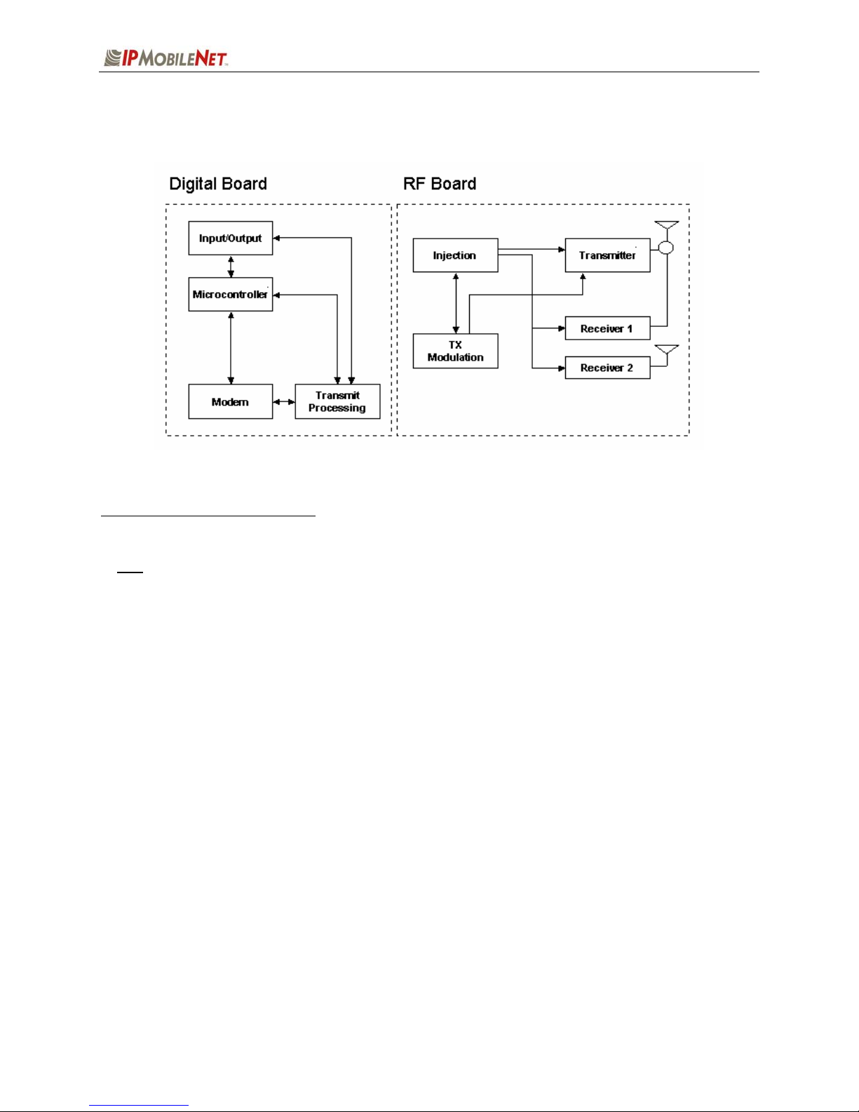
General Block Diagram
General Block Diagram Definitions
For increased data security, the modem supports the Federal Government developed Digital
Encryption Standard (DES) data encryption and decryption protocols. This capability requires
installation of third party, Internet Protocol (IP) compliant DES encryption and decryption
software on the system.
The IPM8 mobile radio is comprised of two (2) circuit boards, the digital board and the RF board. The
digital circuit board contains the following sections:
Input/Output Circuitry associated with the radio’s DB9 data connector providing all the
Microcontroller Manages the operation of the radio, the modem, and determines which
Modem Converts serial data into an analog audio waveform for transmission and
Power Supply The power supply creates the various voltages required by the digital
RS232 data and handshake functions, including the necessary level
changes.
receiver provides a better signal from a given transmission. Also provides
transmit time-out protection in the event a fault causes the radio to halt in
the transmit mode.
analog audio from the receiver to serial data. Within a single chip it
provides forward error detection and correction, bit interleaving for more
robust data communications, and third generation collision detection and
correction capabilities.
portion of the mobile radio.
IPM8-FCCRpt.doc Page 3

SECTION 1: THEORY OF OPERATION
The RF circuit board contains the following sections:
Transmit Processing Circuitry that amplifies the analog audio signal from the modem and uses it
to modulate the voltage controlled oscillator (VCO) and 10 MHz reference
oscillator in the injection synthesizer section. Modulating the VCO and
reference oscillator simultaneously results in a higher quality FM signal.
Injection Synthesizer Provides programmable, ultra stable signals for the radio. Synthesizer
incorporates phase lock loop technology used for both receiving and
transmitting.
Injection In the receive mode, the synthesizer provides a local oscillator signal of 45
MHz above or below the selected receive channel frequency.
Transmitter Consists of an exciter and power amplifier module. The transmitter covers
the various frequency bands in segments. A different power amplifier
module is required for each segment. The transmitter circuitry includes a
T/R switch switching the antenna between transmitter and receiver 1
(TX/RX1).
Receiver 1/Receiver 2 Required to support the mobile DRS; two (2) discrete receivers are tuned
to the same channel and use two (2) antennas.
The receivers are double-conversion superheterodyne with a first
Intermediate Frequency (IF) of 45 MHz and a second IF frequency of 455
KHz. Each receiver consists of bandpass filters, an RF amplifier, a MMIC
mixer, crystal filters, and a one-chip IF system. The injection synthesizer
provides the first local oscillator signal. Outputs from each receiver include
RSSI and analog audio for the baseband routing circuitry and modem.
Power Supply Consists of circuitry that derives the various operating voltages for the RF
portion of the mobile radio.
IPM8-FCCRpt.doc Page 4

SECTION 1: THEORY OF OPERATION
IPM8 Mobile Radio Section Descriptions
The IPM8 Mobile Radio works within a frequency range of 806 to 821 MHz and requires a 1/4-wavelength
This section provides detailed descriptions of each of the sections within the IPM8 Mobile Radio. Refer to
Appendix A to view the IPM8 Mobile Radio Circuit Board Diagram.
Microcontroller
The microcontroller (U30) is a major component of the radio as it manages the operation of the radio. It
also controls the operation of the modem, and determines which receiver provides a better signal from a
given transmission. It provides transmit time-out protection in the event a fault causes the radio to halt in
the transmit mode. It utilizes a reduced instruction set computer (RISC) architecture which provides low
power operation and a powerful instruction set. Other features include a watchdog timer, serial universal
asynchronous receiver/transmitter (UART), two 8-bit timers, and 2 KB of electrically erasable
programmable read only memory (EEPROM) storage.
NOTE
Support circuitry
The support circuitry consists of the following:
A Supervisor Control Chip (U25) provides power-on reset.
The clock controls microcontroller operation and is generated by crystal Y3 and a Pierce oscillator
The latch (U28) decodes low order address bits (A0-A7) from the address/data bits (AD0-AD7). It is
A 512Kx8 Static RAM Chip (U31) provides temporary storage of the radio’s configuration data
Control logic is also an important part in the microcontroller section. The RAM chip select (RAMCS*)
Input/Output
Input/output components convert serial and handshake data from the modem section to RS232 levels,
and vice-versa. Chip U22 is an RS232 transmitter and receiver. It converts data in 5-volt logic form to
data in +/-12-volt form, as required by the RS232 standard. A charge pump power supply on the chip
converts the +5-volt DC logic power on pin 26 to the +12-volt and –12-volt levels required. Capacitors
C106-C109 generate these voltages by a charge pump. These values determine the operating voltages.
antenna.
: The EEPROM Random Access Memory (RAM) stores the setup data entered by the
technician even if there is a loss of power.
circuit (inside the U30-microcontroller).
controlled by Address Latch Enable (ALE) output of U30 and the bits are used by the modem.
facilitating the technician with access to make changes.
and modem chip select (MODEMCS*) command lines are created by U26A, U27BCD, and U44ABC.
These gates decode four (4) high order address bits (A11-A15). The RAM is addressed by five (5)
memory addresses (MA14-MA18) bits decoded by U26D, U27A, and U24. This logic decodes port
address bits (PA14-PA18) to produce memory address bits (MA14-MA18) for the RAM chip.
IPM8-FCCRpt.doc Page 5

SECTION 1: THEORY OF OPERATION
Modem
The single-chip modem circuit converts parallel data to an analog audio waveform for transmission and
analog audio from a receiver to parallel data. In addition to the modem functions, the chip provides
forward error detection and correction (FEC), bit interleaving and Viterbi Soft Decision Algorithms for
more robust data communications.
The microcontroller section controls the modem operation. Address bus, address/data bus, and control
lines operate the modem chip. The modem circuitry is also run by a crystal-controlled clock, which
consists of crystal Y1 and an internal Pierce oscillator.
The received audio signal is demodulated into digital data appearing on the AD0-AD07 lines when the
MODEMCS* and RD* lines are low. The data goes to the microcontroller section for futher processing,
and then to the input/output section for conversion to RS232 or Ethernet signal levels.
During a transmission, outgoing data appearing on the AD0-AD07 lines is converted into a 4-level FSK
analog signal by the modem chip. This operation takes place when the MODEMCS* and WR* lines are
low. Data from the user’s MDC or VIU passes through the input/output section and microcontroller
section to the AD0-AD07 bus. After processing, data passes through a root raised cosine filter and is
output to TXMOD.
This modem supports 115.2 KBPS (serial port), 19.2 KBPS and 32 KBPS (over-the-air) data transmission
rates.
VLogic and Digital Ground
The VLogic and Digital Ground section consists of a pulse-width modulation (PWM) step-down DC-DC
converter (U20) that provides an adjustable output. It also reduces noise in sensitive communications
applications and minimizes drop out voltage.
An external Schottky diode (D2) is required as an output rectifier to pass inductor current during the
second half of each cycle to prevent the slow internal diode of the N-channel MOSFET from turning on.
This diode operates in pulse-frequency modulation (PFM) mode and during transition periods while the
synchronous rectifier is off.
IPM8-FCCRpt.doc Page 6

SECTION 1: THEORY OF OPERATION
Receiver 1 Front-End
This section contains components that include several RF Bandpass filters, a low-noise amplifier, and a
MMIC mixer.
Incoming signals pass through one (1) pre-selector band pass filter (FL3) that selectively provides a high
degree of out-of-band signal rejection. An RF amplifier (U35) amplifies the selected signals and is
followed by a SAW filter (FL4). The output from FL4 passes through a mixer (U4). U4 is a MMIC mixer
which mixes the receive injection (RXINJ1) signal from the synthesizer and the RF signal from the
antenna to produce a 45 MHz IF signal. This 45 MHz signal passes through a matched pair of monolithic
filters (FLT3 and FLT4) to the Receiver 1 IF section to provide the bulk of the Receiver’s selectivity.
Receiver 2 Front-End operates identical to Receiver 1 Front-End.
Receiver 1 IF
The major contributor of the IF subsystem (U34) a complete 45 MHz superheterodyne receiver chip
incorporating a mixer/oscillator, two limiting intermediate frequency amplifiers, quadrature detector,
logarithmic received signal strength indicator (RSSI), voltage regulator and audio and RSSI op amps.
Incoming 45 MHz signals appearing at RX1_45MHz pass through the low-voltage high performance
monolithic FM IF system. Within U34, the signals pass through a simple LC filter and are boosted by the
RF amplifier. The output of the RF amplifier drives a mixer. A crystal oscillator is controlled by crystal Y5
and provides the injection frequency for the mixer. The mixer output passes through a 455 KHz ceramic
filter (FL8). It is then amplified and passed through another ceramic filter (FL7) to a second gain stage.
The IF output drives a quadrature detector. The phase shift elements for the detector are a capacitor
(C140) and a ceramic filter (FLT6). The RSSI detector converts the AGC voltage generated inside the
chip into a DC level corresponding logarithmically to the signal strength. The Diversity Reception
Controller uses BRSSI1 to select the receiver with the best quality signal.
The audio is amplified by a quad rail-to-rail op amp (U19D) and delivered to the power and analog ground
circuitry via the RXMOD1 output. High frequency de-emphasis is provided by a filter consisting of a
resistor and a capacitor. In order to match the audio signal levels with the other circuitry, a gain control is
included. A pot (R99) is necessary to adjust gain.
Receiver 2 IF operates identical to Receiver 1 IF.
Transmit Modulation
The analog circuitry in this section modulates the Transmitter. The data-bearing audio signal from the
modem appears at TXMOD. The audio is amplified by a quad rail-to-rail op amp (U9D). The output of
U9D drives two (2) amplifiers (U9C and U9B).
The transmitter uses dual-point modulation meaning the modulation is applied both to the VCO as well as
the reference oscillator (VCTCXO).
The upper op amp (U9C) has adjustable gain. The output drives op amp (U9A), which inverts the phase
of the signal. Upon the start of a transmission, the modulating signal passes through to the VCTCXO
reference oscillator in the synthesizer. Some makes of VCTCXO oscillators do not require the modulation
signal to be inverted and a jumper block (JMP1) is provided to accommodate the oscillators.
IPM8-FCCRpt.doc Page 7
 Loading...