

Page 1

M
440000 -- 551122 M
Hzz
H
Baassee SSttaattiioonn
B
Daattaa
D
Raaddiioo
R
Owner’s Manual
Date Prepared:
March 1, 2000
16842 Von Karman Avenue, Suite 200 Irvine, CA 92606
Voice: (949) 417-4590 Fax: (949) 417-4591
Document Control #: DC-95
Version: C-1 (Special Release)
Copyright 2000-2002 IP MobileNet, Inc.
Page 2

TABLE OF CONTENTS
SECTION 1: THEORY OF OPERATION .................................................................................. 3
General Block Diagram ........................................................................................................... 3
General Block Diagram Definitions
DR4B Base Station Data Radio Circuitry
System Controller ................................................................................................ 5
Input/Output ......................................................................................................... 5
Modem Switching................................................................................................. 6
Modem .................................................................................................................6
Diversity Reception Controller .............................................................................6
Receive Signal Strength Indication Comparator .................................................. 7
Baseband............................................................................................................. 8
Receiver Board .................................................................................................... 8
IF Amplifier........................................................................................................... 9
Receiver Injection ................................................................................................ 9
Exciter ................................................................................................................10
Analog Modulation ............................................................................................. 10
Phase Locked Loop ........................................................................................... 11
Power Amplifier.................................................................................................. 11
SECTION 2: FACTORY TEST PROCEDURE ........................................................................12
Equipment List ........................................................................................................... 12
Programming and Configuring the Base Station Data Radio ................................ 13
Adjustment / Alignment Procedure .......................................................................... 14
Receiver Injection
Receiver 1
........................................................................................................ 14
............................................................................................. 14
Diversity Reception Controller
Receive Data
Exciter
............................................................................................................ 16
Power Amplifier
.................................................................................................... 15
................................................................................................ 16
SECTION 3: FCC LABEL ....................................................................................................... 17
DR4B Base Station Data Radio FCC Label Placement ........................................... 17
DR4B Base Station Data Radio FCC Label .............................................................. 17
APPENDIX A: DR4B BASE STATION DATA RADIO CIRCUIT BOARD DIAGRAM ............ 18
................................................................................ 3
....................................................................... 5
.......................................................................... 14
~\Technical Documentation\System Manuals\FCC-Reports\IP1B-FCCRpt.doc Page 2
Page 3
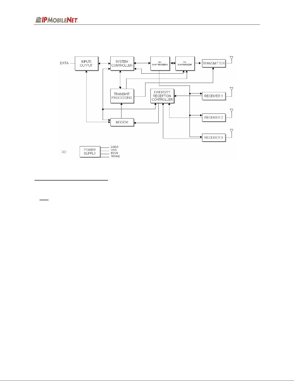
SECTION 1: THEORY OF OPERATION
General Block Diagram
General Block Diagram Definitions
For increased data security, the modem supports the U.S. Government developed Digital Encryption
Standard (DES) data encryption and decryption protocols.
The standard Base Station Data Radio circuit board contains eight (8) sections defined below:
Input/Output Circuitry associated with the base station’s DB25 data connector
System Controller Manages the operation of the base station loading selected transmit/
Includes memory for storage of base station operating parameters.
Transmit Processing Circuitry, which amplifies the analog audio signal from the modem
providing all of the RS232 data and handshake functions, including
the necessary RS232 to logic level changes.
receive frequencies into the injection synthesizer, controls the
operation of the modem and provides transmit timeout protection in
the event a fault causes the radio to become stuck in the transmit
mode.
Electrically erasable programmable read only memory (EEPROM) is
used to store parameters entered by the technician such as channel
numbers and RX/TX frequencies. This information is retained after
power is removed from the base station.
and uses it to modulate a voltage-controlled oscillator (VCO) and
reference oscillator in the transmitter synthesizer section.
Modulating the VCO and reference oscillator simultaneously results
in a higher quality FM signal.
~\Technical Documentation\System Manuals\FCC-Reports\DR4B-FCCRpt.doc Page 3
Page 4

SECTION 1: THEORY OF OPERATION
Modem Converts parallel data into an analog audio waveform for
transmission and analog audio from the receiver to serial data.
Serial data appears on the base station’s DB25 serial port.
The radio supports a 115.2 KBPS data transmission rate on the
serial port, SLIP protocol, and a 19.2 KBPS OR 9.6 KBPS over-theair data transmission rate.
Within a single chip the modem provides forward error correction and
detection, bit interleaving for more robust data communications, and
third generation collision detection and correction capabilities.
Synthesizers Provides ultra stable signals for the three (3) receivers and the
transmitter. Two (2) independent synthesizers are used in the base
station to obtain full duplex (simultaneous receive and transmit)
operations. Both synthesizers incorporate phase lock loop (PLL)
technology and use separate reference oscillators.
RX Synthesizer The receive synthesizer provides a local oscillator signal 45 MHz
above or below the desired receive channel frequency. This is called
high side injection or low side injection.
TX Synthesizer The transmit synthesizer produces the desired frequency by
controlling a VCO. The VCO and the reference oscillator are both
frequency modulated by the modem output.
Diversity Reception Controller Circuitry selects one of three diversity receiver audio outputs for
processing by the modem by comparing the Received Signal
Strength Indication (RSSI) output from each receiver. Essentially,
audio from the receiver with the highest RSSI value is passed on to
the modem.
Transmitter Consists of an exciter and a power amplifier module covering various
frequency bands in segments. A different power amplifier module is
required for each segment. The transmitter power control is included
with the power supply circuitry on the same board.
Receiver 1/Receiver 2/ Uses three (3) discrete receivers tuned to the same frequency.
Receiver 3 The three (3) receivers are required to support IPMN’s base station
DRS.
NOTE
The receivers are double-conversion superhetrodynes with an
Power Supply Power supply circuitry derives the various operating voltages
: Some installations use only two (2) receivers.
Intermediate Frequency (IF) of 45 MHz. Each receiver consist of
bandpass filters, RF amplifiers, a mixer, 45 MHz crystal filter, and a
one-chip IF system. The injection synthesizer provides the first local
oscillator signal and outputs from each receiver including RSSI and
analog audio for the diversity reception controller.
required by the base station. Fixed voltage regulators are employed
through the radio for this purpose.
~\Technical Documentation\System Manuals\FCC-Reports\DR4B-FCCRpt.doc Page 4
Page 5

SECTION 1: THEORY OF OPERATION
DR4B Base Station Data Radio Circuitry
The DR4B Base Station Data Radio works within the frequency range of 400-512 MHz.
The following section provides detail views, descriptions, and key areas on the DR4B Base Station Data
Radio circuit board especially useful during troubleshooting.
System Controller
This section displays the Central Processing Unit (CPU)(U1), clock, and power-on reset circuitry. It
provides more processing power than required for future capabilities to be incorporated into the radio
without changing processors. Such capabilities include data encryption/decryption (DES), remote fault
monitoring, etc. U1 features a 16-bit address bus and 128K of internal flash random access memory
(RAM). To enter the programming mode it is necessary to reset the switch (S1) and power up again.
CPU operations are controlled by Y2 an 4.9152 MHz clock module. Capacitor (C1) and an internal
Schmidt trigger circuit inside of U1 generates the power on reset signal. The RESET* output from U1
drives a latch and decoder found elsewhere on the board.
This section displays the RAM, decoder, EEPROM, and programming power supply circuitry. U2 is a
512K x 8 bit static RAM chip, which provides temporary storage of radio configuration data while the
power is on. This is necessary in order to program the radio configuration. U2 is controlled directly by the
address, data, and control busses from the CPU.
Chip U5 decodes the A11-A14 address bus to provide chip selects for the modem and EEPROM
memory. Chip U6 is an 8-bit latch. It latches inputs from the D0-D7 bus and lights the front panel status
indicators (
Chip U3 is a serial EEPROM, which provides 2K bits of pre-programmed data storage for the CPU. Data
is clocked out of U3 by EECLK, and back into the CPU via EEDATA.
A programming power supply is required for the flash RAM inside of the CPU, and this function is
performed by U4. This chip is an adjustable voltage regulator with a shutdown control. Resistors R8 and
R9 set the output voltage. When the radio configuration data is to be stored in flash RAM, the CPU
makes VPP_ENABLE high. This turns on the regulator, producing a 12-volt output via VPP for the flash
RAM.
This section displays a dedicated processor and voltage regulator. Chip U7 is an optional processor,
which permits manual keyboard operation of the radio. It is not used, and may not be installed on the
board. Regulator U10 provides 5 volts DC power for all logic circuitry on the System Controller Board.
Input/Output
This section displays the CPU input/output circuitry. Chip U11 is an RS232 transmitter/receiver, which
interfaces the CPU to the Diversity Reception Board via J6. From there, the RS232 data goes directly to
a rear panel DB25 connector. U11 converts 5-volt logic-level data to +/-12 volt data in RS232C form, and
vice-versa. A charge pump power supply on the chip converts the +5 volt DC power to the +/-12 volt
levels required. The charge pump uses capacitors (C28 to C31) to generate voltages.
The RS232 serial port data transmission rate of the base station is 115.2 KBPS.
TX, CD, RX1, RX2, and RX3).
~\Technical Documentation\System Manuals\FCC-Reports\DR4B-FCCRpt.doc Page 5
Page 6

SECTION 1: THEORY OF OPERATION
Modem Switching
This section displays the connector wiring and modem switching circuitry. Connector J2 is routed to the
front-panel TX, CD, and RX1-RX3 LED indicators. The radio will also accept modulation from an external
source (modem or amplified microphone audio).
Modem
This base station uses separate modems for receive and transmit functions so that full-duplex operation
may be obtained. The A0-A1 address bus in addition to the individual read (RD*), write (WR*), and chip
select (MODEMTXCS*) lines control all three (3) modems. Modem operations are timed by Y2, a 4.9152
MHZ clock module.
Modem chip U14 is dedicated to the transmit operation. Data from the D0-D7 bus is read by the chip,
and then converted to a 4-level FSK analog signal, which appears on the TXOUT pin. Op amp U21B
buffers the signal, which becomes the MODEM_TXMOD output. From this point, the signal is routed to
the modulation circuitry on the Exciter Board.
Chip U14 has the ability to demodulate receiver audio, although this capability is not used in most
systems. Incoming data-bearing audio from the Diversity Reception Controller Board (and selected
receiver) appears at DISC_AUDIO. The signal passes through resistor R54 and into the modem chip.
Resistor R52 and capacitor C41 serve as feedback elements, limiting both the gain and bandwidth of an
amplifier within U14. The modem chip demodulates the audio into 8 bits of data, which exit U14 on the
D0-D7 bus.
Chip U14 also provides a bias voltage for the analog circuitry on the Exciter Board. This voltage is about
2.5 volts DC, and it appears on the VBIAS line. The purpose of VBIAS is to bias the Exciter Board analog
circuitry for proper operation. Please note that if this voltage is low or missing, the Exciter Board circuitry
may not work.
Modem chip U15 is dedicated to the receive operation. Incoming data-bearing audio from the Diversity
Reception Controller Board (and selected receiver) appears at DISC_ AUDIO. The signal passes through
resistor R56 and into the modem chip. Resistor R55 and capacitor C46 serve as feedback elements,
limiting both the gain and bandwidth of an amplifier within U15. The modem chip breaks down the audio
into 8 bits of data, which exit U15 on the D0-D7 bus.
Modem chip U16 is also dedicated to the receive operation, although it may not be used in this
application. The operation of U16 is exactly the same as U15.
Diversity Reception Controller Board
This section displays the power supply circuitry and input/output connector wiring. The power supply
consists of a diode (CR1), metal oxide varistor (MOV) (CR2), a fuse (F1), and voltage regulators (VR2
and VR3). 13.8 volts DC from the radio’s power connector appears on the anode of CR1. CR1 provides
reverse polarity protection, while CR2 absorbs any damaging transient spikes, which appear on the
unregulated supply line. F1 provides over-current protection. The SWB+ output powers the remaining
boards in the radio, with the exception of the power amplifier module. VR2 provides a 5-volt DC source
for all of the circuitry on the Diversity Reception Controller Board. VR3 provides 5 volts DC for the three
receiver boards via a connector (TB1).
Two (2) 16-pin DIP headers connect this board to the System Controller Board. One header (J2)
provides power and control signals for the System Controller Board. The ALARMA and ALARMC lines
are of particular interest because the base station has optional external fault monitoring capabilities. For
~\Technical Documentation\System Manuals\FCC-Reports\DR4B-FCCRpt.doc Page 6
Page 7

SECTION 1: THEORY OF OPERATION
example, if a fault in the base station site produces a contact closure on one of the alarm inputs, the radio
transmits a fault message to the Communication Center. Examples of faults include site door open, high
temperature, high VSWR, etc. Upon receipt of the fault message, a technician is dispatched to the base
station site to correct the fault. In order to obtain these capabilities, monitoring software must be loaded
into the System Controller Board CPU and the Internet Protocol Network Controller (IPNC).
Another header (J1) routes RS232 data, clock, and handshake signals from the System Controller Board
to DB25 interface connector (J3). This connector is physically mounted on the rear panel of the base
station.
This section displays the level shifters for the three (3) receivers. Each receiver provides a DC voltage
received signal strength indication (RSSI) corresponds to the signal strength of an incoming signal. The
RSSI output from receiver 1 appears at RSSI1. It passes through low pass filter R13 and C16. The low
pass filter capacitor (C16) minimizes RF pickup by the op amp. An op amp (U11B) provides amplification
and a DC level shift. An additional op amp (U11C) provides additional amplification. Resistors (R3 and
R4) and a pot (R11) set gain of the op amp. The DC offset is injected into U11C via a pot (R12) and a
resistor (R5). The amplified and level shifted output leaves the op amp as SHIFT_ RSSI1 and goes to a
comparator circuit.
The remaining level shifters work in the same manner.
Individual gain and DC offset pots are provided so that minor RSSI performance differences between the
Receive Signal Strength Indication Comparator
This section displays the RSSI comparator circuitry. It uses a two-step selection process to determine
which receiver has the strongest signal, as follows:
The receiver 1 and receiver 2 RSSIs are compared, and the strongest receiver is selected.
The selected receiver’s RSSI and receiver 3 RSSI are compared, and the strongest is selected. The
A comparator (U5) looks at the RSSI1 and RSSI2 inputs. When RSSI1 is greater than RSSI2, the
comparator output goes high, and a LED (D1) lights to indicate receiver 1 was selected. At the same
time, the RX1/RX2_SELECT line goes high, which activates the solid-state switch (U8). This causes the
receiver 1 RSSI signal to be routed to a second comparator. Otherwise, if the receiver 2 RSSI is greater
than receiver 1, the RX1/RX2_SELECT line goes low, and another LED (D2) lights to indicate receiver 2
was selected. U8 simply routes receiver 2 RSSI to a second comparator (U10). The digital
RX1/RX2_SELECT output controls a switch.
U10 looks at the selected receiver (RSSI1/RSSI2) and RSSI3 inputs. Should RSSI3 be greater than the
other input, the comparator output goes high, and LED (D3) lights to show receiver 3 is selected. At the
same time, another switch (U6) connects RSSI3 to the analog SEL_RSSI output. The digital
RX3_SELECT output controls a switch. Otherwise, if the selected receiver’s RSSI is greater than RSSI3,
the comparator output remains low making the RX3_SELECT output low. U6 simply connects the
selected receiver’s analog RSSI signal to the SELRSSI output.
A chip (U3) forms a comparator circuit. When the RSSI voltage exceeds a threshold, a LED (D4) lights.
Like the other three (3) LEDs, this circuit is intended as a diagnostic tool. It provides a go/no go indication
that an RF signal has been received. A pot (R74) sets the turn-on voltage.
three receivers can be trimmed out.
circuitry provides two (2) digital outputs and an analog RSSI voltage from the selected receiver.
~\Technical Documentation\System Manuals\FCC-Reports\DR4B-FCCRpt.doc Page 7
Page 8

SECTION 1: THEORY OF OPERATION
Baseband
This circuitry amplifies the audio from each receiver, routes it through solid-state switches, and selects the
audio from the receiver with the highest quality value. The comparator circuit on the previous sheet
controls it.
There are three (3) channels of audio, with separate gain and DC offset adjustments to compensate for
performance differences in the receivers. For example, incoming audio from receiver 1 appears at
AUDIO 1. An op amp (U12D) is then amplifies the audio. A pot (R72) adjusts the gain. The amplifier
output drives a switch (U4).
The remaining audio circuits work in the same manner.
Two (2) solid-state switches route audio from the selected receiver. U4 selects audio from either
Receiver 1 or 2. When the RX1/RX2_SELECT input from the comparator circuitry is high, Receiver 1
audio is passed through the device. Another switch (U7) selects audio from either a selected Receiver (1
or 2) or receiver 3. When the RX3_SELECT input from the comparator circuitry is high, Receiver 3’s
audio is passed through the device. The output from U7 appears on DISC_AUD, which goes to a header
(J2). From there the audio is demodulated by the modems on the System Controller Board.
The radio also offers a voice grade audio output via the rear panel DB25 connector. DISC_AUD also
drives low pass filter (U14), and buffer (U9D). The AUDIO OUT line from the buffer goes to pin 12 of a
connector (J3).
This section displays manual receiver switching and DC power distribution. Manual receiver switching is
primarily intended as a diagnostic tool. By closing various switches on S1, the RX1/RX2_SELECT or
RX3_SELECT LINES may be forced high or low, as appropriate. This overrides the operation of the
comparator circuitry, forcing one receiver to operate at all times. Resistors (R98 and R97) provide power
supply short circuit protection in the event the wrong switches are closed.
Pads (TP4 and TP5) represent the power distribution bus (TP4 and TP5). Incoming power from the rear
panel fuse holder appears on pad TP4. The B+ output goes to the power supply circuitry. TP5 connects
to the transmitter power amplifier.
Receiver Board
Please be aware that the radio uses three (3) identical receiver boards. As a result, the circuitry will be
Front end. Incoming signals pass through a filter (FT1). The filter (FT1) is a double-tuned device, which
provides a high degree of selectivity. The desired signals are amplified by U4, a low noise amplifier.
Additional selectivity is provided by triple-tuned filter (FT2). An RF amplifier (Q1) amplifies the signal.
The output from Q1 passes through triple-tuned filter (FT3), and then to mixer (U5). U5 is a doublebalanced mixer, which heterodynes a local oscillator signal from the Injection Synthesizer Board. The IF
output leaves the mixer as the 45 MHz line. It goes to an IF filter on the following sheet.
There are five (5) filter sets (FT1, FT2, and FT3) available, and each covers a 20-30 MHz
described only once.
portion of the UHF band. Should replacement of the filters be required, exact replacement
parts must be used.
~\Technical Documentation\System Manuals\FCC-Reports\DR4B-FCCRpt.doc Page 8
Page 9

SECTION 1: THEORY OF OPERATION
IF Amplifier
The incoming 45 MHz signal passes through Y5, a highly selective monolithic bandpass filter. From there
the IF signal passes through an LC matching network. C17, C18, C24, and L5 provide impedance
matching to the IF amplifier input. U6 is a super heterodyne IF subsystem. Inside the chip, the signal is
applied to a mixer. The mixer also accepts a 44.545 MHz local oscillator input. The local oscillator
consists of an internal amplifier, plus crystal (Y4) and associated components. The mixer output passes
through Y3, a 455 KHz ceramic IF filter. It is amplified, passed through ceramic filter (Y2), and on to a
second IF stage. The IF output drives a quadrature detector. The recovered audio appears at pin 9,
while RSSI appears at pin 7.
Within the RSSI circuitry, chip U6 uses a detector, which converts if the current is generated inside the
chip into a DC level corresponding logarithmically to signal strength. RSSI is used by the Diversity
Reception Controller to select the receiver with the highest quality signal.
The audio is buffered by op amp U3A. From there the AUDIO output line goes to a connector, for hookup
to the Diversity Reception Controller Board.
The RSSI is buffered by op amp U3B. From there the RSSI output line goes to a connector, for hookup
to the Diversity Reception Controller Board.
Several sets of 455 KHz IF filters (Y3 and Y2) are available to suit receiver selectivity requirements.
Should replacement of these filters be required, exact replacement parts must be used.
Receiver Injection
The Injection Synthesizer Board provides a highly stable local oscillator signal for the three receivers. A
synthesizer on the board develops the signal.
This displays a serial data input/output interface, synthesizer, and VCO. The I/O interface circuitry
accepts clock, serial data, and enable signals from the System Controller Board via terminal block TB1. A
lock detect (LD) status output is returned to the System Controller Board from the synthesizer. U3 is a
hex Schmidt Trigger inverter, which squares up incoming signals for reliable operation of the synthesizer
chip. This is necessary because of a cable run between the two (2) boards.
The main section of this board is synthesizer chip (U2). The device contains the key components of a
phase locked loop (PLL), including a 1.1 GHz prescaler, programmable divider, and phase detector. In
operation, the desired frequency is loaded into U2 as a clocked serial bit stream via the CLK and DATA/I
inputs. The lock detection circuitry consists of inverters U3E/U3F, diode CR3, and resistor R5. When the
synthesizer is in lock, the LD pin on U2 is high, making the LD output on terminal block TB1 high. The
EXC LD input on TB1 routes the lock detect output from the Exciter Board through diode CR3, and out
through LD. This configuration tells the CPU on the System Controller Board that it is acceptable to
process received data, or to key the transmitter when LD is high. Otherwise, if a fault in either synthesizer
prevents a lock, receive and transmit operation will be inhibited.
The UHF injection signal is generated by module VCO1. This device is a wide-range voltage controlled
oscillator (VCO). A voltage on the VT input determines the VCO frequency. The voltage is generated by
the phase detector output (PD/O) of U2, which drives a loop filter consisting of R4, C19, C20, R21 and
C10. The filter integrates the pulses, which normally appear on PD/O into a smooth DC control signal for
the VCO. The output of VCO1 is attenuated by module AT1, resulting in improved VCO stability.
~\Technical Documentation\System Manuals\FCC-Reports\DR4B-FCCRpt.doc Page 9
Page 10

SECTION 1: THEORY OF OPERATION
This section displays the DC power supplies, frequency reference, and RF output circuitry. Regulator
VR1 provides 9 volts DC for VCO module VCO1, and RF amplifier (U7). Regulator (VR2) provides a low
noise 5-volt DC output for inverter (U3), synthesizer (U2), and reference (Y1).
Reference module (Y1) provides a high-stability 10 MHz reference frequency. Y1 is a voltage controlled,
temperature controlled crystal oscillator (VCTCXO). This device also has a VC input which accepts a
control voltage from pot R23. The pot permits a slight shift in the reference frequency which enables the
three (3) receivers to be tuned precisely to the assigned receive frequency. A diode (CR2) provides
additional voltage regulation, improving the frequency stability of reference Y1.
The RF output circuitry consists of RF amplifier (U7), and power splitters (U5 and U6). U7 increases the
signal level to correct for losses in the splitters. One output drives splitter U5, which provides local
oscillator injection for Receivers 2 and 3. The other output drives splitter (U6), which drives receiver 1
and the PLL_FEEDBACK input on chip U2.
Exciter Board
This section displays the input/output interface, transmitter keying, and power supply circuitry. The
input/output interface is built around terminal block (TB1) and Schmidt Trigger inverters (U7). Incoming
clock, serial data, and chip select signals on block TB1 are squared up by U7. Then they are sent to the
appropriate inputs on the transmitter synthesizer (U2). The EXCDATA source comes from the receive
synthesizer on the Injection Synthesizer Board. A Schmidt Trigger chip is used here because of a cable
ran to the System Controller Board. The synthesizer returns a lock detect output to the Injection
Synthesizer Board via U6 and EXCLD.
A regulator (VR2) powers the T/R switch circuitry. When the System Controller Board makes TXKEY*
low, inverter U6D goes high, turning on transistor Q2 and FET Q1. This applies 5-volt power to the
TXENABLE output, turning on the T/R switch on the Power Amplifier Board. At the same time, transistor
Q3 conducts, grounding the KEY* input of the Power Amplifier Board. Finally, inverter U6C goes high
and turns on RF switch U1, connecting the VCO output to the Power Amplifier Board for transmission.
The power supply consists of two (2) voltage regulators. A regulator (VR1) provides 5-volt power for the
VCO.
Analog Modulation
This section displays the analog modulation circuitry. Incoming modem audio from the System Controller
Board appears at TXMOD, and is buffered by op amp U5C. If an external modulation source (modem or
amplified microphone) is connected to the base station’s DB25 connector, audio appears at EXTMOD.
From there the audio passes through low pass filters U10, U4DCBA, and on to the input of op amp U5B.
The audio is inverted and amplified by an op amp (U5B). It then passes on to the VCO module via
VCOMOD.
The 10 MHz reference is also modulated in order to counteract the corrective effects of the synthesizer
loop circuitry. For example, if only the VCO were modulated, the synthesizer would try to compensate for
the frequency “error,” caused by the modulation. This effectively reduces the amount of modulation
available. Modulating the reference and the VCO simultaneously effectively cancels this effect when the
reference frequency goes high, the VCO frequency goes high, and vice-versa.
An op amp (U9A) amplifies the AUDIO output from another op amp (U5D) and applies it to jumper block
JMP1. Pot R30 adjusts the gain of U9A. Op amp (U9B) inverts the phase of the audio and applies it to
the other side of jumper block JMP1. The purpose of the jumper block is to select the proper phase of the
audio. If the wrong phase is used, on modulation peaks the reference will swing in the same direction as
~\Technical Documentation\System Manuals\FCC-Reports\DR4B-FCCRpt.doc Page 10
Page 11

SECTION 1: THEORY OF OPERATION
the VCO, canceling out most of the modulation. The output from the jumper block goes to the 10 MHz
reference via REFMOD.
The VBIAS input is a 2.5-volt DC source, which biases the op amps to the correct operating point. It is
generated by modem chip (U14) on the System Controller Board.
Phase Locked Loop
This section displays phase locked loop (PLL) circuitry. The 10-MHz reference (Y1), runs synthesizer
(U2), which in turn controls VCO1. The main section of this board is the synthesizer chip (U2). The
device contains the key components of a PLL, including a 1.1 GHz prescaler, programmable divider, and
phase detector.
In operation, the desired frequency is loaded into U2 as a clocked serial bit stream via the CLK and
DATA/I inputs. The lock detection circuitry consists of inverters U6A and U6B, diode CR1, and resistor
R1. When the synthesizer is in lock, the LD pin on U2 is high, making the EXCLD output on terminal
block (TB1) high. The EXCLD output on TB1 routes the lock detect output from the Exciter Board. This
configuration tells the CPU on the System Controller Board that it is acceptable to process received data,
or to key the transmitter when LD is high. Otherwise, if a fault in either synthesizer prevents a lock,
receive and transmit operation will be inhibited.
The switch (JMP1) is used to select the supply voltage to chip U2. The UHF injection signal is generated
by module VCO1. This device is a wide-range voltage controlled oscillator (VCO). A voltage on the VT
input determines the VCO frequency. The voltage is generated by the phase detector output (PD/O) of
U2, which drives a loop filter consisting of R19, C16, C17, and C47. The filter integrates the pulses,
which normally appear on PD/O into a smooth DC control signal for the VCO. The output of VCO1 is
attenuated by module AT2, resulting in improved VCO stability.
Amplifier U8 amplifies the signal and applies it to a splitter (U3). One output of U3 is connected to a
switch (U1). U1 is enabled by signal TX when the transmitter is enabled. The other output of the splitter
is connected through AT1 and provides feedback to U2.
Power Amplifier
The transmit injection signal from the RF injection section is applied to the high-powered linear amplifier
(U1) one (1) watt amplifier. The signal is then routed to the final power amplifier boosting the output
signal to 40 watts. The output of the amplifier is routed to transmit antenna port ANT1 (via SW1).
~\Technical Documentation\System Manuals\FCC-Reports\DR4B-FCCRpt.doc Page 11
Page 12

SECTION 2: FACTORY TEST PROCEDURE
Equipment List
The following table lists the equipment required to perform the DT450 Mobile Data Radio Factory Test Procedure:
QTY DESCRIPTION MANUFACTURER MODEL
PC’s
2
1
1 Digital multi-meter
1
1 4-Channel Scope Tektronix TDS 460A
1 DR4B Calibrated Base Station
1
1 100 watt dummy load/attenuator Pasternack
2 UHF Antennas (generic mag mount)
1
1 DT power cable
One for Mobile
One for Base
Service Monitor – Communication Test
Set
DC power supply w/ ammeter, 13.8V,
12 Amps or more
Internet Protocol Network Controller
(IPNC)
Serial cable DB25M-DB25F
connectors
Windows 9X w/
IPMessage
AVR
HP
Tektronix
Fluke
Astron
HP890 or
equivalent
77 or
equivalent
VS12M or
equivalent
PE7021-40 or
equivalent
1
1
1 Ceramic tuning tool
1 ea
3-foot RF jumper cable with type N
connectors (generic)
Scope test probe (generic, X1
attenuation)
#0, #1, and #2 Phillips screwdrivers
(generic)
IPMN p/n:
44010006
~\Technical Documentation\System Manuals\FCC-Reports\DR4B-FCCRpt.doc Page 12
Page 13

SECTION 2: FACTORY TEST PROCEDURE
Programming and Configuring the Base Station Data Radio
Once the appropriate equipment for performing the factory test are gathered, perform the following steps
to rpgoram and configure the DR4B Base Station Data Radio:
Step 1 Enter the following information on the Base Station Data Radio Performance Test Data
Sheet:
Base Station Serial number
Date test being performed
Tester’s name
Step 2 At the HyperTerminal window, type in the appropriate password and press [ENTER].
Step 3 Type ? and press [ENTER]. The following example displays in the HyperTerminal
window:
Host serial = 115200,N,8,1, timeout=200
Host framing = SLIP, no split frames no status messages
tunnel = 0
TX format = new
Injection = LOW SIDE, 45MHz
channel spacing = 25000
Channel = 0
Channel Tx freq Rx freq Inj freq
Frequency=0 , 481.000000, 486.000000, 441.000000
Serial number: yyyyyyyyy
RIM address = 1
Frequency group = 1
TX quiet time = 5
Symbol sync time = 12 milliseconds, 0 extra inter-split-frame count
TX tail time = 5
Radio data rate = 19200
Max data tx time = 60 seconds
Carrier detect delay time = 1 millisecond
Station ID = ABC123
Station ID time =10 minutes
Polarity = TX+, RX+
Allow crc errors = 0
Suppress keep alive = 0
Allow base to base = 0
Timeslot status = 0
Duplicate time = 10 milliseconds
Control head grant delay = 50 milliseconds
RIM DD delay = 0 milliseconds
Retry interval = 0 milliseconds
Retry time limit = 0 milliseconds
RSSI step = 25 (=19dBm)
IPNC = 192.168.3.3
SLIP Address = 192.168.4.6
RF IP Address = 192.168.3.1
SNTP interval = 60 seconds
num timeslots = 16
timeslot period = 992ms
timeslots per voice packet = 4
noise = -128dBm
Fixed TX Delay = 0 milliseconds
Scale TX Delay = 0 microseconds
~\Technical Documentation\System Manuals\FCC-Reports\DR4B-FCCRpt.doc Page 13
Page 14

SECTION 2: FACTORY TEST PROCEDURE
Adjustment / Alignment Procedures
Receiver Injection
Perform the following steps to adjust the receiver injection and injection frequency:
Step 1 Using the HP high frequency probe, verify that the receiver injection frequency is
Step 2 Adjust R7 on the receiver injection circuit board to set the injection frequency within 10
Receiver 1
Step 1 Using the high frequency probe, monitor the 44.545 MHz second injection frequency
Step 2 Inject an on-frequency signal at a level of –80 dBm, modulated with a 1 KHz test tone at
Step 4 While monitoring RSSI at TB1-4 with the digital multi-meter, adjust the trimmer capacitor
Step 5 Check the receiver’s distortion and verify that it is less than 3%.
Step 6 Adjust C1 slightly if necessary for minimum distortion.
Step 7 Check the receiver’s sensitivity, verifying that the SINAD is 12 dB or better at a maximum
Step 8 Repeat procedure for Receivers 2 and 3.
Diversity Reception Controller
Step 1 Inject an on-frequency signal at a level equal to Receiver 1 12dB SINAD level, modulated
Step 2 While monitoring TP1 with the digital multi-meter, adjust RSSI1 low adjust potentiometer
Step 3 Increase the amplitude of the signal by 50 dBm.
Step 4 While monitoring TP1 with the digital multi-meter, adjust RSSI1 high adjust potentiometer
Adjustments R11 and R12 are interactive adjustments, therefore continue adjustments until the DC voltage
at TP1 is 0.750 VDC for the receiver’s 12 dB SINAD level and 2.75 VDC for a 50 dBm increase from the
receiver’s 12 dB SINAD level.
present at each of the three (3) receivers by monitoring the receivers’ R12 surface mount
pad which lies on the 50 ohm track between L3 and U3.6.
Hz of the exact injection frequency. The amplitude of the injection frequency should read
approximately +5 dBm ±1 dBm.
at U2 pin 3, adjust trimmer capacitor (C5) to the center of the oscillator’s oscillation
range. The amplitude level of pin 3 of U2 should read between +5 and +10 dBm.
±5.0 KHz deviation into the receiver under test.
(C1) for maximum RSSI. The RSSI properly tuned receiver should be approximately 2.8
to 3.4 VDC.
level of –119 dBm (-120 is typical).
with a 1 KHz test tone at ±5.0 KHz deviation into Receiver 1.
(R12) for a reading of 0.750 VDC ±10 mV.
(R11) for a reading of 2.75 VDC ±10 mV.
~\Technical Documentation\System Manuals\FCC-Reports\DR4B-FCCRpt.doc Page 14
Page 15

SECTION 2: FACTORY TEST PROCEDURE
Step 5 Inject an on-frequency signal at a level equal to Receiver 2 12dB SINAD level, modulated
with a 1 KHz test tone at ±5.0 KHz deviation into Receiver 2.
Step 6 While monitoring TP2 with the digital multi-meter, adjust RSSI2 low adjust potentiometer
(R10) for a reading of 0.750 VDC ±10 mV.
Step 7 Increase the amplitude of the signal by 50 dBm.
Step 8 While monitoring TP2 with the digital multi-meter, adjust RSSI2 high adjust potentiometer
(R9) for a reading of 2.75 VDC ±10 mV.
Adjustments R9 and R10 are interactive adjustments, therefore continue adjustments until the DC voltage
at TP2 is 0.750 VDC for the receiver’s 12 dB SINAD level and 2.75 VDC for a 50 dBm increase from the
Step 9 Inject an on-frequency signal at a level equal to Receiver 3 12dB SINAD level, modulated
Step 10 While monitoring TP3 with the digital multi-meter, adjust RSSI3 low adjust potentiometer
Step 11 Increase the amplitude of the signal by 50 dBm.
Step 12 While monitoring TP3 with the digital multi-meter, adjust RSSI3 high adjust potentiometer
Adjustments R33 and R35 are interactive adjustments, therefore continue adjustments until the DC voltage
Step 13 Adjust the carrier detect potentiometer (R74) to illuminate a level of –116 dBm.
Receive Data
Step 1 Using a calibrated mobile radio, generate uplink data messages using the X=2000,19
Step 2 Attach an antenna to one of the base station’s receiver ports and verify on the base
receiver’s 12 dB SINAD level.
with a 1 KHz test tone at ±5.0 KHz deviation into Receiver 3.
(R33) for a reading of 0.750 VDC ±10 mV.
(R35) for a reading of 2.75 VDC ±10 mV.
at TP3 is 0.750 VDC for the receiver’s 12 dB SINAD level and 2.75 VDC for a 50 dBm increase from the
receiver’s 12 dB SINAD level.
command in the IP Message Utility program (see the Internet Protocol (IP) Data
Transceiver IP4/IP8 System Manual for instructions).
station monitor screen (HyperTerminal) that the received message data quality are
consistently 240 and higher for 2000 character messages. Repeat test for each receiver.
Constant fluctuations in the data quality are indicative of group delay programs. The data
quality readings should always be at or above 240.
~\Technical Documentation\System Manuals\FCC-Reports\DR4B-FCCRpt.doc Page 15
Page 16

SECTION 2: FACTORY TEST PROCEDURE
Exciter
Step 1 Using the X=2000,19 command, generate data messages so the transmit power and
frequency can be checked.
Step 2 Connect the base stations' transmit port to the HP communication test set. Note the
power level prior to adjusting.
Step 3 On the power amplifier circuit board adjust the potentiometer (RV1) fully clockwise (this
will enable low power transmit operation).
Step 4 While transmitting data messages using the X=2000,19 command, adjust the following:
TCXO Y1 and R14 for minimum frequency error
R11 for ±5.0 KHz deviation
Transmit output power should be approximately 1mWatt. The REFMOD adjustment needs to be made
Step 5 Connect the base station to the IPNC.
Step 6 Using a calibrated mobile radio operating on the base station’s channel, adjust R4 for
This command will ping the IPNC continuously with a 500-character test message. Press [Ctrl]+C to
Power Amplifier
Step 1 Connect the base stations' transmit port to the communication test set.
Step 2 Using the X=2000,19 command, generate data messages.
Step 3 Slowly increase the base station output power by turning the power control potentiometer
Do not exceed 20 watts output power as this will reduce the life of the amplifier module.
Step 4 Perform a close visual inspection of the radio paying close attention to manufacturing
while the base station is transmitting real data messages to and from a mobile radio. This is most easily
done using the ping command to ping the IPNC from a mobile radio. This will cause the base station to
repeatedly send data messages and will facilitate the REFMOD adjustment.
consistent data quality readings of 248 (as observed on the mobile radio’s attached PC
IP Message window). Access the MSDOS prompt and ping using the following
command:
>;ping 192.168.3.3 –t -l 500 –w 2000
stop the ping.
counterclockwise until the power noted previously or 40 Watts of output power is
obtained or to the level.
related problems such as loose screws, solder practices, etc.
~\Technical Documentation\System Manuals\FCC-Reports\DR4B-FCCRpt.doc Page 16
Page 17

DR4B Base Station Data Radio FCC Label Placement
DR4B Base Station Data Radio FCC Label Placement
SECTION 3: FCC LABEL
~\Technical Documentation\System Manuals\FCC-Reports\DR4B-FCCRpt.doc Page 17
Page 18
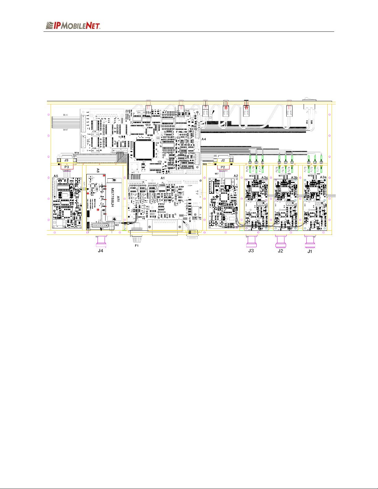
APPENDIX B: DR4B CIRCUIT BOARD DIAGRAM
~\Technical Documentation\System Manuals\FCC-Reports\DR4B-FCCRpt.doc Page 18
 Loading...