

IPMobileNet B32150-25, IP8B Product Owners Manual

P
Seerriieess
IIP
S
B3322115500--2255
B
PPrroodduucctt O
16842 Von Karman Avenue, Suite 200 Irvine, CA 92606
Voice: (949) 417-4590 Fax: (949) 417-4591
O
Date Released: December 4, 2003
Document #: 516.80517.POM
Copyright 2003 IPMobileNet, Inc.
Baassee SSttaattiioonn
B
wnneerr’’ss
w
Version: X1
.
Maannuuaall
M

The term “IC”: before the radio certification number only signifies that Industry of Canada
technical specifications were met.
Operation is subject to the following two (2) conditions: (1) this devise may not cause
interference, and (2) this device must accept any interference, including interference that may
cause undesired operation of this device.
The following U.S. Patents apply to this product:
U.S. Patent numbers 5,640,695,6,018,647,6,243,393
Information contained in this document is subject to change without notice.
All rights reserved. Reproductions, adaptations, or translation without prior written permission is
prohibited, except as allowed under copyright laws.
402004 Page ii

TABLE OF CONTENTS
SECTION 1: THEORY OF OPERATION .................................................................................................... 4
General Block Diagram.................................................................................................................. 4
General Block Diagram Definitions
Input/Output ........................................................................................................... 4
System Controller................................................................................................... 4
Modems
........................................................................................................... 5
Diversity Reception
RX Injection............................................................................................................ 5
Transmitter ............................................................................................................. 5
Receiver 1/ 2/ 3...................................................................................................... 5
Power Supply......................................................................................................... 5
B32150-25 Base Station Section Descriptions ........................................................................... 6
System Controller
Input/Output
Modem Switching
Modem
...............................................................................................................................7
................................................................................................................ 6
........................................................................................................................ 6
................................................................................................................ 6
Receive Signal Strength Indication Comparator
Baseband ............................................................................................................................ 8
Receiver Board ................................................................................................................... 8
IF Amplifier
.......................................................................................................................... 8
Receiver Injection................................................................................................................ 9
Exciter Board....................................................................................................................... 9
Analog Modulation
............................................................................................................ 10
Phase Locked Loop .......................................................................................................... 10
Power Amplifier................................................................................................................. 11
SECTION 2: FCC LABEL.......................................................................................................................... 12
B32150-25 Base Station FCC Label Placement ........................................................................12
B32150-25 Base Station FCC Label............................................................................................ 12
APPENDIX A: B32150-25 CIRCUIT BOARD DIAGRAM.......................................................................... 13
APPENDIX B: B32150-25 TEST DATA SHEET........................................................................................ 17
..................................................................................... 4
.......................................................................................... 5
................................................................. 7
402004 Page 3
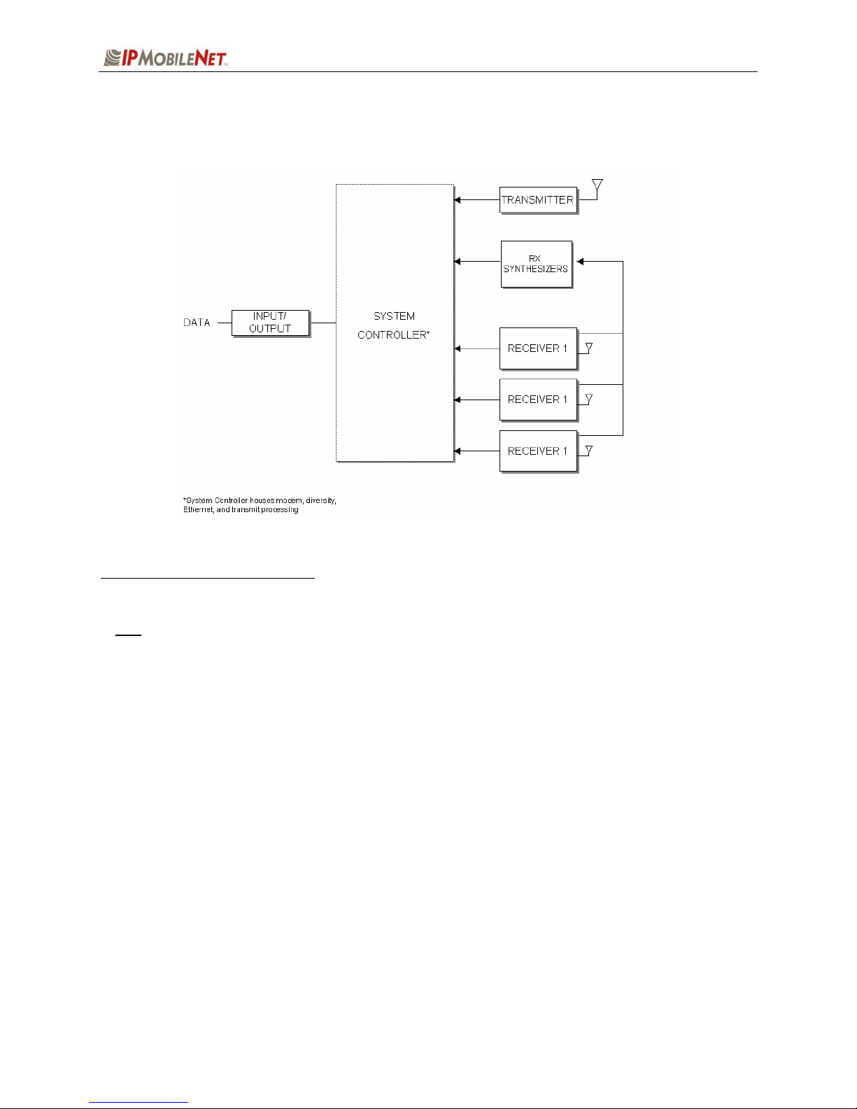
SECTION 1: THEORY OF OPERATION
GENERAL BLOCK DIAGRAM
General Block Diagram Definitions
For increased data security, the modem supports the U.S. Government developed Digital Encryption
Standard (DES) data encryption and decryption protocols. This capability requires installation of thirdparty IP compliant DES encryption and decryption software.
The standard IPSeries base station circuit board contains five (5) main sections defined below:
Input/Output Circuitry associated with one of the following base station’s data
connectors:
RS232 Serial Port DB9 Data Connector
RJ45 Ethernet 10 Base T Interface Connection
System Controller Houses the modem, diversity, and Ethernet circuitry. Manages the
operation of the base station’s modem providing transmit timeout
protection in the event a fault causes the base station to become
halted in the transmit mode. The system controller also handles the
loading of selected transmit and receive frequencies into the injection
synthesizer. Includes memory for storage through Electrically
Erasable Programmable Read Only Memory (EEPROM) of the base
station’s operating parameters, which are retained after the base
stations power is cycled off.
402004 Page 4

SECTION 1: THEORY OF OPERATION
Modems Convert data into an analog audio waveform for transmission and
analog audio from the receiver to serial data interface. There is one
(1) modem that is dedicated to the transmit operation and two (2)
modems dedicated to the receive operation. The modem dedicated
to the transmit supports a 115.2 KBPS data transmission rate on the
serial port, SLIP protocol, and a 32 KBPS over-the-air data
transmission rate. Provides Forward Error Correction (FEC) and
Error Detection (CRC), bit interleaving for more robust data
communications, and third generation collision detection and
correction capabilities.
Diversity Reception
RX Injection The Injection Synthesizer board provides a highly stable local
Transmitter Consists of an exciter and a power amplifier module covering various
Receiver 1/Receiver 2/ Uses three (3) discrete receivers tuned to the same frequency.
Receiver 3 The three (3) receivers are required to support IPMobileNet’s base
NOTE
The receivers are double-conversion superhetrodynes with an
Power Supply Power supply circuitry derives the various operating voltages
Circuitry selects one of three (3) diversity receiver audio outputs for
processing by the modem by comparing the Received Signal
Strength Indication (RSSI) output from each receiver. Audio from the
receiver with the highest RSSI value is passed to the modems.
oscillator signal for the three (3) receivers. This displays a serial
data input/output interface, synthesizer, and VCO.
frequency bands in segments. A different power amplifier module is
required for each segment. The transmitter power control is included
with the power supply circuitry on the same board.
station Diversity Reception System (DRS).
: Some installations use only two (2) receivers.
Intermediate Frequency (IF) of 45 MHz. Each receiver consist of
bandpass filters, RF amplifiers, a mixer, 45 MHz crystal filter, and a
one-chip IF system. The injection synthesizer provides the first local
oscillator signal and outputs from each receiver including RSSI and
analog audio for Diversity Reception.
required by the base station. Fixed voltage regulators are employed
through the base station for this purpose.
402004 Page 5

SECTION 1: THEORY OF OPERATION
B32150-25 Base Station Section Descriptions
System Controller
This section displays the Central Processing Unit (CPU)(U1), clock, and power-on reset circuitry. It
provides more processing power than required for future capabilities to be incorporated without changing
processors. Such capabilities include data encryption/decryption (DES) and remote fault monitoring. U1
features a 16-bit address bus and 128K of internal flash random access memory (RAM).
NOTE
: To enter the programming mode it is necessary to reset the switch (S1) and power up again.
CPU operations are controlled by Y3 an 18.432 MHz clock module. Capacitor (C1) and an internal
Schmidt trigger circuit inside of U1 generates the power on reset signal. The RESET* output from U1
drives a latch and decoder found elsewhere on the board.
This section displays the RAM, decoder, EEPROM, and programming power supply circuitry. U2 is a
512K x 8 bit static RAM chip, which provides temporary storage of base station configuration data while
the power is on. This is necessary in order to program the base station. U2 is controlled directly by the
address, data, and control busses from the CPU.
Chip U5 decodes the A11-A14 address bus to provide chip selects for the modem and EEPROM
memory. Chip U6 is an 8-bit latch. It latches inputs from the D0-D7 bus and lights the front panel status
indicators (
TX, CD, RX1, RX2, and RX3).
Chip U3 is a serial EEPROM, which provides 2K bits of pre-programmed data storage for the CPU. Data
is clocked out of U3 by EECLK, and back into the CPU via EEDATA.
A programming power supply is required for the flash RAM inside of the CPU, and this function is
performed by U4. This chip is a low dropout voltage regulator with a shutdown control. Resistors R22
and R21 set the output voltage. When the base station configuration data is to be stored in flash RAM,
the CPU makes VPP_ENABLE high. This turns on the regulator, producing a 12-volt output via VPP for
the flash RAM.
This section displays a dedicated processor and voltage regulator. Chip U7 is a processor, which permits
manual keyboard operation of the base station. Regulator VR2 provides 5 volts DC power for all logic
circuitry on the System Controller Board.
Input/Output
This section displays the CPU input/output circuitry. Chip U8 is an RS232 transceiver, which interfaces
the CPU to the modem via J1. From there, the RS232 data goes directly to a rear panel DB9 connector.
U8 converts 5-volt logic-level data to +/-12 volt data in RS232C form, and vice-versa. A charge pump
power supply on the chip converts the +5 volt DC power to the +/-12 volt levels required. The charge
pump uses capacitors (C28 to C31) to generate voltages.
NOTE
: The RS232 serial port data transmission rate of the base station is 115.2 KBPS.
Modem Switching
This section displays the connector wiring and modem switching circuitry. Connector J7 is routed to the
front-panel TX, CD, and RX1-RX3 LED indicators. The base station will also accept modulation from an
external source (modem or amplified microphone audio). Transmission gate U10A switches this signal
source.
402004 Page 6
 Loading...