

查询ST300S04M3供应商
PHASE CONTROL THYRISTORS Stud V ersion
Bulletin I25158 rev. B 01/94
ST300S SERIES
Features
Center amplifying gate
Hermetic metal case with ceramic insulator
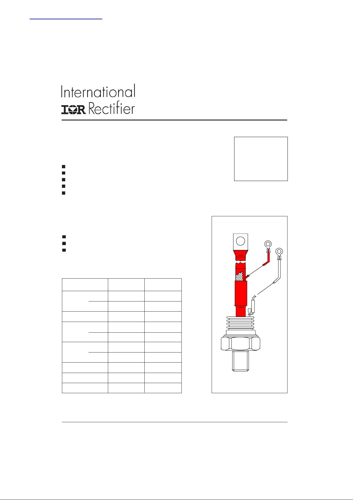
International standard case TO-209AE (TO-118)
Threaded studs UNF 3/4 - 16UNF2A or ISO M24x1.5
Compression Bonded Encapsulation for heavy duty
operations such as severe thermal cycling
Typical Applications
DC motor controls
Controlled DC power supplies
AC controllers
Major Ratings and Characteristics
Parameters ST300S Units
I
T(AV)
I
T(RMS)
I
TSM
@ T
C
@ 50Hz 8000 A
@ 60Hz 8380 A
300 A
75 °C
470 A
300A
I2t@
V
DRM/VRRM
t
q
T
J
50Hz 320 KA2s
@ 60Hz 292 KA
typical 100 µs
www.irf.com
400 to 2000 V
- 40 to 125 °C
2
s
case style
TO-209AE (TO-118)
1
ST300S Series
Bulletin I25158 rev. B 01/94
ELECTRICAL SPECIFICATIONS
Voltage Ratings
Voltage V
DRM/VRRM
Type number Code peak and off-state voltage repetitive peak voltage @ T
04 400 500
08 800 900
ST300S 50
12 1200 1300
16 1600 1700
18 1800 1900
20 2000 2100
On-state Conduction
Parameter ST300S Units Conditions
I
Max. average on-state current 300 A 180° conduction, half sine wave
T(AV)
@ Case temperature 75 ° C
I
Max. RMS on-state current 470 A DC @ 64°C case temperature
T(RMS)
I
Max. peak, one-cycle 8000 t = 10ms No voltage
TSM
non-repetitive surge current 8380 t = 8.3ms reapplied
2
t Maximum I2t for fusing 320 t = 10ms No voltage Initial TJ = TJ max.
I
2
I
√t Maximum I2√t for fusing 3200 KA2√s t = 0.1 to 10ms, no voltage reapplied
Low level value of threshold
V
T(TO)1
voltage
High level value of threshold
V
T(TO)2
voltage
r
Low level value of on-state
t1
slope resistance
High level value of on-state
r
t2
slope resistance
V
Max. on-state voltage 1.66 V Ipk= 940A, TJ = TJ max, tp = 10ms sine pulse
TM
I
Maximum holding current 600
H
I
Typical latching current 1000
L
, max. repetitive V
, maximum non- I
RSM
DRM/IRRM
VVmA
6730 t = 10ms 100% V
7040 t = 8.3ms reapplied Sinusoidal half wave,
292 t = 8.3ms reapplied
226 t = 10ms 100% V
207 t = 8.3ms reapplied
0.97 (16.7% x π x I
0.98 (I > π x I
0.74 (16.7% x π x I
0.73 (I > π x I
A
KA2s
V
mΩ
mA T
RRM
RRM
< I < π x I
T(AV)
),TJ = TJ max.
T(AV)
< I < π x I
T(AV)
),TJ = TJ max.
T(AV)
= 2 5 ° C , anode supply 12V resistive load
J
), TJ = TJ max.
T(AV)
), TJ = TJ max.
T(AV)
max.
= TJ max
J
2
www.irf.com
Switching
Parameter ST300S Units Conditions
di/dt Max. non-repetitive rate of rise Gate drive 20V, 20Ω, t
of turned-on current T
t
Typical delay time 1.0
d
Typical turn-off time 10 0
t
q
1000 A/µs
µs
= TJ max, anode voltage ≤ 80% V
J
Gate current 1A, dig/dt = 1A/µs
= 0.67% V
V
d
= 550A, TJ = TJ max, di/dt = 40A/µs, VR = 50V
I
TM
dv/dt
DRM, TJ
= 20V/µs, Gate 0V 100Ω, t
Blocking
Parameter ST300S Units Conditions
dv/dt Maximum critical rate of rise of
off-state voltage
Max. peak reverse and off-state
I
RRM
leakage current
I
DRM
500 V/µs TJ = TJ max. linear to 80% rated V
50 mA TJ = TJ max, rated V
ST300S Series
Bulletin I25158 rev. B 01/94
≤ 1µs
r
DRM
= 25°C
= 500µs
p
DRM
DRM/VRRM
applied
Triggering
Parameter ST300S Units Conditions
PGMMaximum peak gate power 10.0 TJ = TJ max, tp ≤ 5ms
P
Maximum average gate power 2.0 TJ = TJ max, f = 50Hz, d% = 50
G(AV)
I
Max. peak positive gate current 3.0 A TJ = TJ max, tp ≤ 5ms
GM
+V
Maximum peak positive
GM
gate voltage
Maximum peak negative
-V
GM
gate voltage
20
5.0
TYP. MAX.
I
DC gate current required TJ = - 40°C
GT
to trigger mA T
200 100 200
50 -
VGTDC gate voltage required TJ = - 40°C
to trigger V TJ = 25°C
2.5 -
1.8 3
1.1 -
I
DC gate current not to trigger 10.0 mA
GD
VGDDC gate voltage not to trigger 0.25 V
W
VTJ = TJ max, tp ≤ 5ms
= 25°C
J
TJ = 125°C
T
= 125°C
J
T
= TJ max
J
Max. required gate trigger/ current/ voltage are the lowest value
which will trigger all units 12V
anode-to-cathode applied
Max. gate current/ voltage not to
trigger is the max. value which
will not trigger any unit with rated
anode-to-cathode applied
V
DRM
www.irf.com
3

ST300S Series
Bulletin I25158 rev. B 01/94
Thermal and Mechanical Specification
Parameter ST300S Units Conditions
TJMax. operating temperature range -40 to 125
Max. storage temperature range -40 to 150
T
stg
R
Max. thermal resistance,
thJC
junction to case
R
Max. thermal resistance,
thCS
case to heatsink
T Mounting torque, ± 10% 48.5
wt Approximate weight 535 g
Case style TO - 209AE (TO-118) See Outline Table
∆R
Conduction
thJC
(The following table shows the increment of thermal resistence R
0.10 DC operation
0.03 Mounting surface, smooth, flat and greased
(425)
Conduction angle Sinusoidal conduction Rectangular conduction Units Conditions
180° 0.011 0.008 T
120° 0.013 0.014
90° 0.017 0.018 K/ W
60° 0.025 0.026
30° 0.041 0.042
°C
K/W
Nm
Non lubricated threads
(lbf-in)
when devices operate at different conduction angles than DC)
thJC
J
= TJ max.
Ordering Information Table
Device Code
1 - Thyristor
2 - Essential part number
3 - 0 = Converter grade
4 - S = Compression bonding Stud
5 - Voltage code: Code x 100 = V
6 - P = Stud base 16UNF threads
M = Stud base metric threads (M24 x 1.5)
7 - 0 = Eyelet terminals (Gate and Auxiliary Cathode Leads)
1 = Fast - on terminals (Gate and Auxiliary Cathode Leads)
3 = Threaded top terminal 3/8" 24UNF-2A
8 - Critical dv/dt: None = 500V/µsec (Standard value)
4
ST 30 0 S 20 P 0
(See Voltage Rating Table)
RRM
L = 1000V/µsec (Special selection)
53 4
7 812 6
www.irf.com

Outline Table
AMP. 280000-1
REF-250
CERAMIC HOUSING
RED SILICON RUBBER
38 (1.50)
MAX. DIA.
22 (0.87) MAX.
4.3 (0.17) DIA.
10.5 (0.41)
NOM.
RED CATHODE
WHITE GATE
FLEXIBLE LEAD
2
C.S. 50mm
(0.078 s.i.)
4.5 (0.18) MAX.
ST300S Series
Bulletin I25158 rev. B 01/94
.
N
I
M
)
7
3
.
0
(
5
.
9
.
N
I
M
)
6
8
.
0
(
2
2
Fast-on Terminals
245 ( 9.65)
255 (1 0.04)
RED SHRINK
MAX.
27.5 (1 . 0 8 )
49 (1.92) MAX.
* FOR METRIC DEVICE: M24 X 1.5 - LENGHT SCREW 21 (0.83) MAX.
WHITE SHRINK
SW 45
3/4"16 UNF-2A
MAX.
47 ( 1.85)
21 (0.82) MAX.
Case Style TO-209AE (TO-118)
with top thread terminal 3/8"
All dimensions in millimeters (inches)
245 (9.65) ± 10 (0.39)
CERAMIC HOUSING
25 (0.98)
77.5 (3.05)
80.5 (3.17)
MAX.
27.5 (1.08)
Case Style TO-209AE (TO-118)
All dimensions in millimeters (inches)
17 (0.67) DIA.
3/8"-24UNF-2A
38 (1.5)
DIA. MAX.
MAX.
47 (1.85)
MAX.
21 (0.83)
SW 45
www.irf.com
3/4"-16UNF-2A *
* FOR METRIC DEVICE: M24 x 1.5 - LENGHT SCREW 21 (0.83) MAX.
5

ST300S Series
Bulletin I25158 rev. B 01/94
130
120
ST 300S Ser ies
R (DC) = 0.10 K/W
thJC
110
100
Conduction A ngle
30°
90
80
70
Maximum Allowable Case Temperature (°C)
0 50 100 150 200 250 300 350
60°
90°
120°
Average On-state Current (A)
Fig. 1 - Current Ratings Characteristics
480
440
400
360
320
280
180°
120°
90°
60°
30°
RMS Limit
240
200
160
120
80
40
0
Maximu m A v er a ge On-state Power Lo s s (W )
0 40 80 120 160 200 240 280 320
Average On-state Current (A)
130
120
110
100
90
80
180°
Conduction Angl e
ST 300S S er ies
T = 125°C
J
0
.
0
8
0
.
1
2
K
/
0.
2
K
/
0
.
3
K
/
0
.
4
K
/
0
.
6
K
/
1
.
2
K
/
70
60
Maximu m Allowa ble Case Tempera tur e (°C)
0 100 200 300 400 500
R
t
h
S
K
A
/
W
=
0
.
0
W
W
W
W
W
W
3
25 50 75 100 125
Maximum Allowa ble Ambi ent Temperatu re (°C )
Fig. 3 - On-state Power Loss Characteristics
ST30 0S Series
R (DC) = 0.10 K/W
thJC
Conduction Period
30°
60°
90°
120°
180°
DC
Average On-state Current (A)
Fig. 2 - Current Ratings Characteristics
K
/
W
D
e
l
t
a
R
650
600
550
500
450
400
350
300
250
200
150
100
50
Maximum Average On-state Power Loss (W)
DC
180°
120°
90°
60°
30°
RMS Limit
0
0
100 200 300 400 500
Average On-state Current (A)
Conduct ion P eriod
ST 300S Se r ie s
T = 125°C
J
R
t
h
S
A
= 0
.
0
0
0
.
0
0
0
1
3
.
0
1
2
.
2
.
3
.
6
2
.
K
8
/W
K
/
K
/
K
/
K
/
K
/
K
/
-
W
W
W
W
W
W
D
e
lta R
25 50 75 100 125
Max im u m Al lowabl e Amb i en t Tem per ature (°C)
Fig. 4 - On-state Power Loss Characteristics
6
www.irf.com

ST300S Series
Bulletin I25158 rev. B 01/94
7500
At Any Rated Load Condition And With
Rated V Appli ed Following Surge.
7000
6500
6000
RRM
Initial T = 125°C
J
@ 60 Hz 0.00 83 s
@ 50 Hz 0.01 00 s
5500
5000
4500
4000
ST300S Series
3500
Peak Half Sine Wave On-state Current (A)
3000
110100
Number Of Equ al Amp litude Half C ycle C urren t Pulses ( N )
10000
T = 25°C
J
1000
Peak Half Sine Wave On-state Current (A)
T = 125°C
J
8500
Maximum Non Repetitive Surge Current
8000
7500
7000
6500
6000
5500
5000
4500
4000
3500
3000
Versus Pulse Train Duration. Control
Of Conduc tion Ma y N ot Be Maint a ined.
ST300S Series
0.01 0.1 1
Pulse Train Duration (s)
Initi al T = 125 °C
No Voltage Reapplied
Rated V Reapplied
RRM
Fig. 6 - Maximum Non-Repetitive Surge CurrentFig. 5 - Maximum Non-Repetitive Surge Current
J
thJC
0. 001
Transient Thermal Impedance Z (K/W)
www.irf.com
ST 300S S eries
Instantaneous On-state Current (A)
100
0123456789
Instant aneous On-state Voltage ( V)
Fig. 7 - On-state Voltage Drop Characteristics
1
Steady State Value
R = 0.10 K/W
thJC
(DC Opera t ion )
0.1
0.01
ST 300S Ser ie s
0.001 0.01 0.1 1 10
Square Wave Pulse Duration (s)
Fig. 8 - Thermal Impedance Z
Characteristic
thJC
7

ST300S Series
Bulletin I25158 rev. B 01/94
100
Rectangu lar gate pulse
a) Recommended load line for
rate d di/dt : 20V, 10ohms; tr <=1 µs
b) Recomm en d e d load line for
<=30% rated di/dt : 10V, 10ohms
10
tr<=1 µs
1
Instantaneous Gat e Voltage (V)
0.1
0.001 0.01 0.1 1 10 100
VGD
IGD
Device : ST300S Series
(1) PGM = 10W, tp = 4ms
(2) PGM = 20W, tp = 2ms
(3) PGM = 40W, tp = 1ms
(4) PGM = 60W, tp = 0.66ms
(a)
(b)
Tj=-40 °C
Tj=25 °C
Tj=125 °C
Frequency Limi ted by PG(AV)
Instantaneous Gate Current (A)
Fig. 9 - Gate Characteristics
(1)
(2) (3)
(4)
8
www.irf.com
 Loading...