查询ST083S04PFK0供应商
Bulletin I25185 rev. C 03/03
ST083S SERIES
INVERTER GRADE THYRISTORS
Features
Center amplifying gate
High surge current capability
Low thermal impedance
High speed performance
Typical Applications
Inverters
Choppers
Induction heating
All types of force-commutated converters
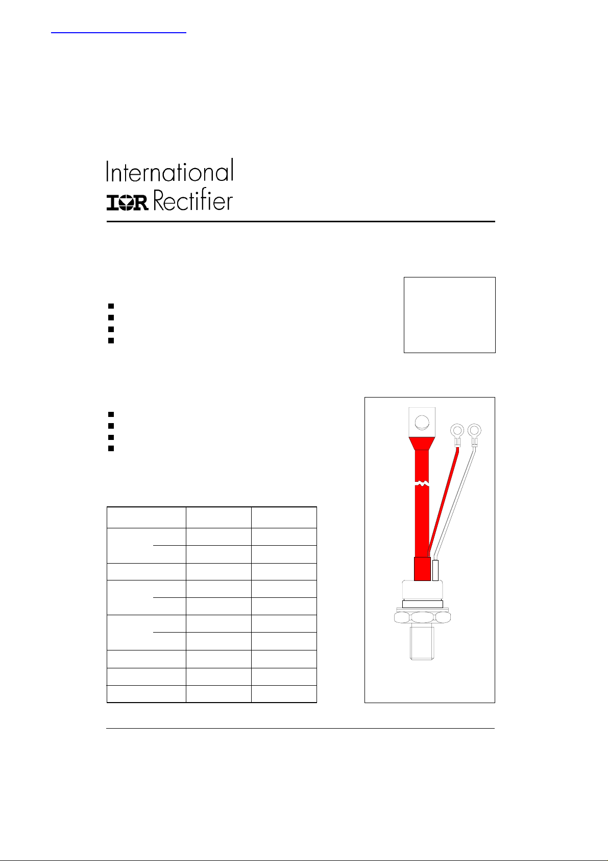
Major Ratings and Characteristics
Parameters ST083S Units
I
T(AV)
I
T(RMS)
I
TSM
@ T
C
@ 50Hz 2450 A
@ 60Hz 2560 A
85 A
85 °C
135 A
Stud Version
85A
I2t@
V
DRM/VRRM
t
range (see table) 10 to 20 µs
q
T
J
50Hz 30 KA2s
@ 60Hz 27 KA2s
400 to 1200 V
- 40 to 125 °C
www.irf.com
case style
TO-209AC (TO-94)
1

ST083S Series
Bulletin I25185 rev. C 03/03
ELECTRICAL SPECIFICATIONS
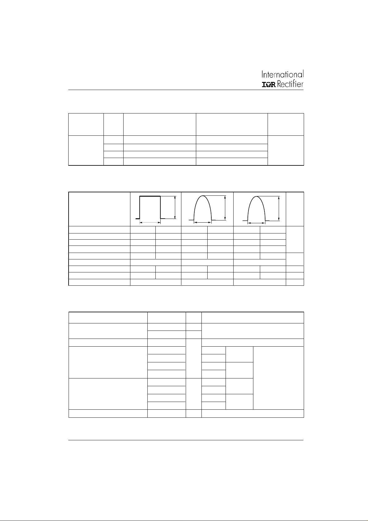
Voltage Ratings
Voltage V
DRM/VRRM
Type number Code repetitive peak voltage non-repetitive peak voltage @ T
04 400 500
ST083S 30
08 800 900
10 1000 1100
12 1200 1300
Current Carrying Capability
, maximum V
, maximum I
RSM
DRM/IRRM
VVmA
max.
= TJ max.
J
I
Frequency Units
180
TM
o
el
180oel
I
TM
I
TM
100µs
50Hz 210 120 330 270 2540 1930
400Hz 200 120 350 210 1190 810
1000Hz 150 80 320 190 630 400 A
2500Hz 70 25 220 85 250 100
Recovery voltage Vr 50 50 50 50 50 50
Voltage before turn-on Vd V
DRM
V
DRM
V
DRM
Rise of on-state current di/dt 50 50 - - - - A/µs
Case temperature 60 85 60 85 60 85 °C
Equivalent values for RC circuit 22Ω / 0.15µF 2 2Ω / 0.15µF 22Ω / 0.15µF
On-state Conduction
Parameter ST083S Units Conditions
I
Max. average on-state current 85 A 180° conduction, half sine wave
T(AV)
@ Case temperature 85 °C
Max. RMS on-state current 13 5 DC @ 77°C case temperature
I
T(RMS)
Max. peak, one half cycle, 2450 t = 10ms No voltage
I
TSM
non-repetitive surge current 2560 A t = 8.3ms reapplied
2060 t = 10ms 100% V
2160 t = 8.3ms reapplied Sinusoidal half wave,
2
I
t Maximum I2t for fusing 30 t = 10ms No voltage Initial TJ = TJ max
27 t = 8.3ms reapplied
21 t = 10ms 100% V
KA2s
19 t = 8.3ms reapplied
2
I
√t Maximum I2√t for fusing 300 KA2√s t = 0.1 to 10ms, no voltage reapplied
RRM
RRM
V
2
www.irf.com

ST083S Series
Bulletin I25185 rev. C 03/03
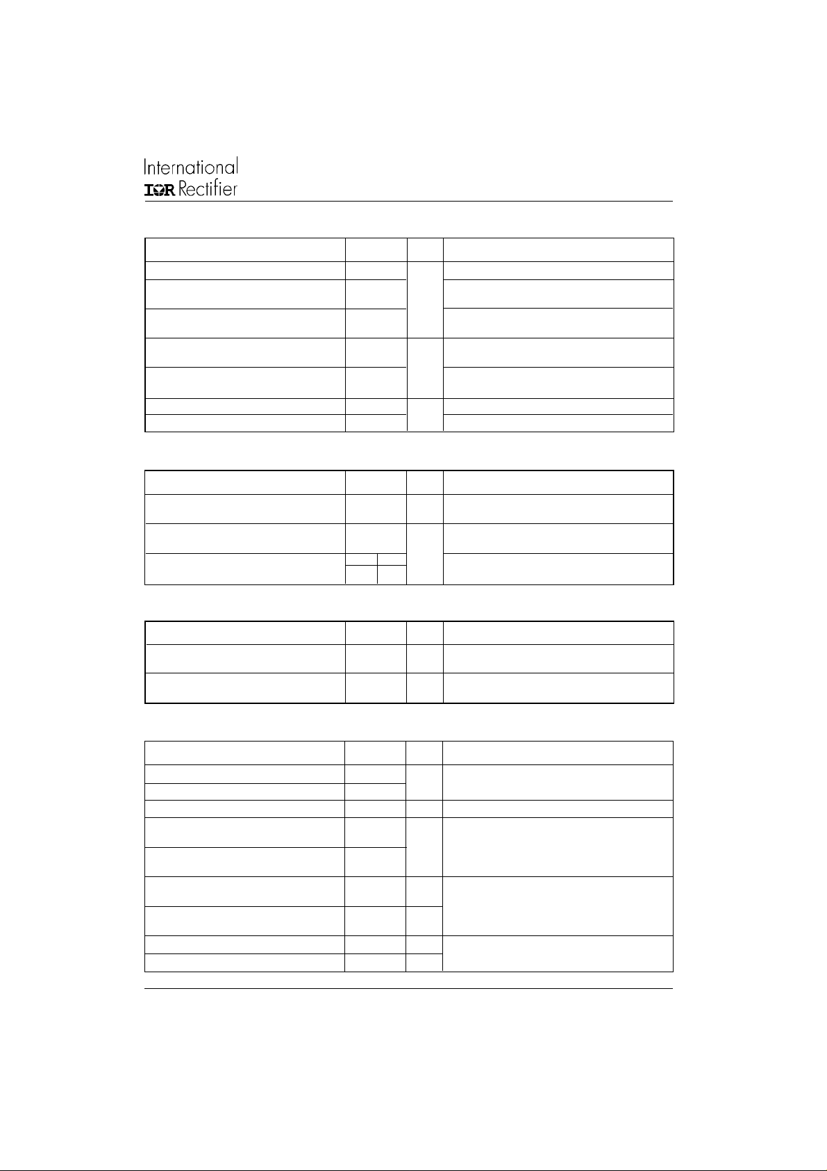
On-state Conduction
Parameter ST083S Units Conditions
VTMMax. peak on-state voltage 2.15 ITM= 300A, TJ = TJ max, tp = 10ms sine wave pulse
Low level value of threshold
V
T(TO)1
voltage
High level value of threshold
V
T(TO)2
voltage
r
Low level value of forward
1
t
slope resistance
High level value of forward
r
2
t
slope resistance
I
Maximum holding current 600 TJ = 25°C, IT > 30A
H
Typical latching current 1000 TJ = 25°C, VA= 12V, Ra = 6Ω, IG= 1A
I
L
Switching
Parameter ST083S Units Conditions
di/dt Max. non-repetitive rate of rise T
of turned-on current I
t
Typical delay time 0.80
d
t
Max. turn-off time 10 20
q
1.46 (16.7% x π x I
V
1.52 (I > π x I
2.32 (16.7% x π x I
mΩ
2.34 (I > π x I
mA
= TJ max, V
1000 A/µs
Min Max
J
= 2 x di/dt
TM
T
= 25°C, V
J
Resistive load, Gate pulse: 10V, 5Ω source
µs
T
= TJ max, I
J
V
= 50V, tp = 200µs, dv/dt = 200V/µs
R
< I < π x I
T(AV)
), TJ = TJ max.
T(AV)
T(AV)
), TJ = TJ max.
T(AV)
DRM
= rated V
DM
= 100A, commutating di/dt = 10A/µs
TM
< I < π x I
= rated V
DRM, ITM
T(AV)
T(AV)
DRM
), TJ = TJ max.
), TJ = TJ max.
= 50A DC, tp= 1µs
Blocking
Parameter ST083S Units Conditions
dv/dt Maximum critical rate of rise of T
off-state voltage available on request
I
Max. peak reverse and off-state
RRM
leakage current
I
DRM
500 V/µs
30 mA T
Triggering
Parameter ST083S Units Conditions
PGMMaximum peak gate power 40
P
Maximum average gate power 5
G(AV)
I
Max. peak positive gate current 5 A TJ = TJ max, tp ≤ 5ms
GM
+V
Maximum peak positive
GM
gate voltage
Maximum peak negative
-V
GM
gate voltage
I
Max. DC gate current required
GT
to trigger
V
Max. DC gate voltage required
GT
to trigger
I
Max. DC gate current not to trigger 20 mA
GD
V
Max. DC gate voltage not to trigger 0.25 V
GD
20
5
200 mA
3V
WT
VTJ = TJ max, tp ≤ 5ms
T
TJ = TJ max, rated V
www.irf.com
= TJ max., linear to 80% V
J
= TJ max, rated V
J
= TJ max, f = 50Hz, d% = 50
J
= 25°C, VA = 12V, Ra = 6Ω
J
DRM/VRRM
applied
DRM
, higher value
DRM
applied
3
 Loading...