

Bulletin I2065 rev. A 09/94
SD253N/R SERIES
FAST RECOVERY DIODES Stud Version
Features
High power FAST recovery diode series
1.5 to 2.0 µs recovery time
High voltage ratings up to 1600V
High current capability
Optimized turn on and turn off characteristics
Low forward recovery
Fast and soft reverse recovery
Compression bonded encapsulation
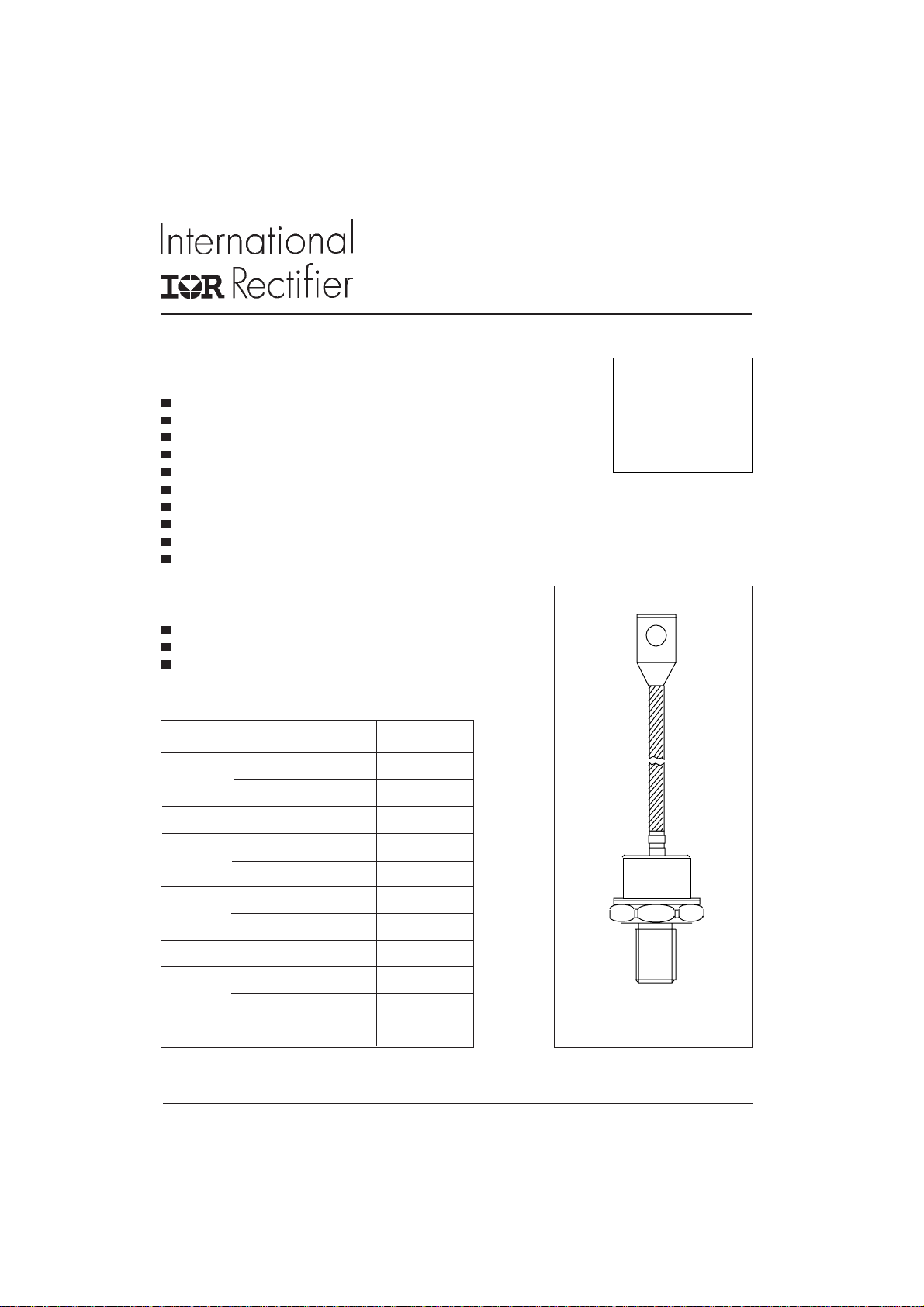
Stud version JEDEC DO-205AB (DO-9)
Maximum junction temperature 125°C
Typical Applications
Snubber diode for GTO
High voltage free-wheeling diode
Fast recovery rectifier applications
250A
Major Ratings and Characteristics
Parameters SD253N/R Units
I
F(AV)
@ T
C
I
F(RMS)
I
FSM
I2t@
V
RRM
trrrange 1.5 to 2.0 µs
T
J
@ 50Hz 5350 A
@ 60Hz 5600 A
50Hz 143 KA2s
@ 60Hz 130 KA
range 400 to 1600 V
@ T
J
www.irf.com
250 A
85 °C
392 A
25 °C
- 40 to 125 °C
2
s
case style
DO-205AB (DO-9)
1
SD253N/R Series
Bulletin I2065 rev. A 09/94
ELECTRICAL SPECIFICATIONS
Voltage Ratings
Voltage V
Type number Code peak and off-state voltage repetitive peak voltage T
04 400 500
SD253N/R..S15 08 800 900
10 1000 1100
12 1200 1300
SD253N/R..S20 14 1400 1500
16 1600 1700
Forward Conduction
Parameter SD253N/R Units Conditions
I
Max. average forward current 250 A 180° conduction, half sine wave.
F(AV)
@ Case temperature 85 °C
I
Max. RMS current 392 A DC @ 74°C case temperature
F(RMS)
Max. peak, one-cycle 5350 t = 10ms No voltage
I
FSM
non-repetitive forward current 5600 t = 8.3ms reapplied
2
I
t Maximum I2t for fusing 143 t = 10ms No voltage Initial TJ = TJ max.
2
I
√t Maximum I2√t for fusing 1430 KA2√s t = 0.1 to 10ms, no voltage reapplied
Low level of threshold voltage 0.87 (16.7% x π x I
V
F(TO)1
High level of threshold voltage 1.17 (I > π x I
V
F(TO)2
r
Low level of forward slope resistance 0.62 (16.7% x π x I
f1
High level of forward slope resistance 0.29 (I > π x I
r
f2
V
Max. forward voltage 1.38 V Ipk= 785A, TJ = 25°C, tp = 400 µs square pulse
FM
max. repetitive V
RRM
, maximum non- I
RSM
VVmA
4500 t = 10ms 100% V
4710 t = 8.3ms reapplied Sinusoidal half wave,
130 t = 8.3ms reapplied
101 t = 10ms 100% V
92 t = 8.3ms reapplied
A
KA2s
V
mΩ
F(AV)
), TJ = TJ max.
F(AV)
F(AV)
), TJ = TJ max.
F(AV)
RRM
RRM
< I < π x I
< I < π x I
), TJ = TJ max.
F(AV)
), TJ = TJ max.
F(AV)
max.
RRM
= 125°C
J
35
Recovery Characteristics
Code
T
= 25 oC
J
typical t
@ 25% I
rr
RRM
Test conditions Max. values @ T
I
pk
Square Pulse @ 25% I
di/dt V
r
t
rr
RRM
(µs) (A) (A/µs) (V) (µs) (µC) (A)
S15 1.5 2.9 90 44
S20 2.0 3.2 107 46
750 25 - 30
= 125 °C
J
QrrI
rr
2 www.irf.com
SD253N/R Series
Bulletin I2065 rev. A 09/94
Thermal and Mechanical Specification
Parameter SD253N/R Units Conditions
T
Max. operating temperature range -40 to 125
J
Max. storage temperature range -40 to 150
T
stg
Max. thermal resistance, junction to case 0.115 DC operation
R
thJC
Max. thermal resistance, case to heatsink 0.08 Mounting surface, smooth, flat and greased
R
thCS
T Mounting torque ± 10% 31 Not lubricated threads
24.5 Lubricated threads
wt Approximate weight 250 g
Case style DO-205AB (DO-9) See Outline Table
∆R
Conduction
thJC
(The following table shows the increment of thermal resistence R
Conduction angle Sinusoidal conduction Rectangular conduction Units Conditions
180° 0.010 0.008 TJ = TJ max.
120° 0.013 0.014
90° 0.017 0.019 K/ W
60° 0.025 0.027
30° 0.044 0.044
°C
K/W
Nm
when devices operate at different conduction angles than DC)
thJC
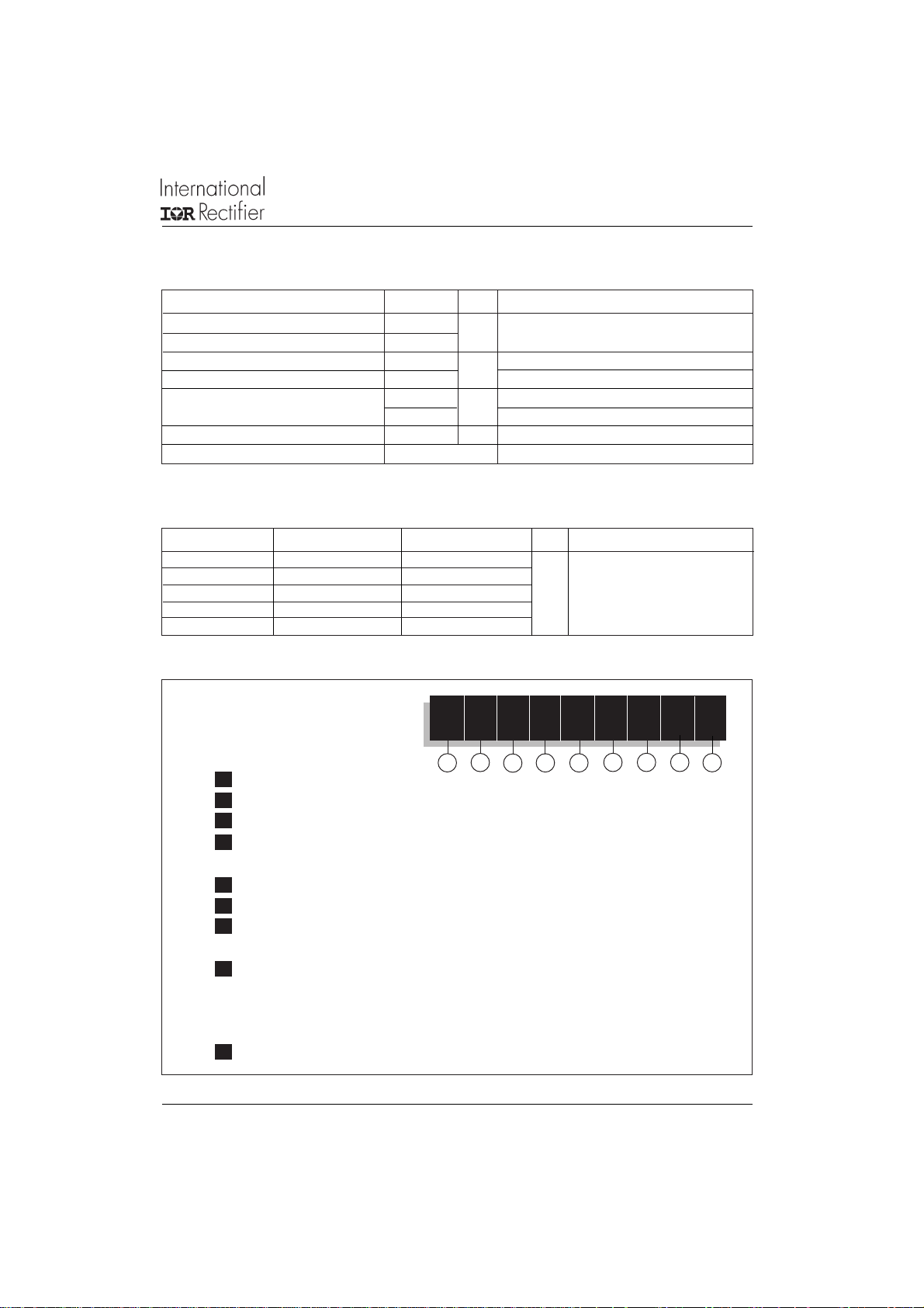
Ordering Information Table
1 - Diode
2 - Essential part number
3 - 3 = Fast recovery
4 - N = Stud Normal Polarity (Cathode to Stud)
R = Stud Reverse Polarity (Anode to Stud)
5 - Voltage code: Code x 100 = V
6 -trr code (see Recovery Characteristics table)
7 - P = Stud base DO-205AB (DO-9) 3/4" 16UNF-2A
M = Stud base DO-205AB (DO-9) M16 X 1.5
8 -7 B = Flag top terminals (for Cathode/ Anode Leads)
S = Isolated lead with silicone sleeve
(Red = Reverse Polarity; Blue = Normal Polarity)
None = Not isolated lead
9 - V = Glass-metal seal
Device Code
SD 25 3 R 16 S20 P B V
2 3 4
(see Voltage Ratings table)
RRM
51
7689
3www.irf.com

SD253N/R Series
Bulletin I2065 rev. A 09/94
Outline Table
GLASS-METAL SEAL
19 (0.75)
MAX.
9.5 ( 0.37) MIN.
4 (0.16) MAX.
MAX.
39 (1.53)
DIA. 8.5 (0.33) NOM.
75 (2.95 ) MIN.
28.5 (1.12)
21 (0.82)
DIA. 28.5 (1.08) MAX.
MAX.
MAX.
16 (0.63)
MAX.
* FOR METRIC DEVICE: M16 X 1.5
3/4-16UNF-2A*
200 (7.87) ± 10 (0.39)
C.S. 35mm
(0.054 s.i.)
SW 32
GLASS-METAL SEAL
70 (2.75) MAX.
2
DIA. 28.5 (1.12) MAX.
MAX.
28.5 (1.12)
Conform to JEDEC DO-205AB (DO-9)
All dimensions in millimeters (inches)
21 (0.83)
16 (0.63)
14 (0.55)
MAX.
DIA. 6.5 (0.26)
13 (0.51)
62 ( 2.4 4)
MAX.
21 (0.83)
DO-205AB (DO-9) Flag
All dimensions in millimeters (inches)
*FOR METRIC DEVICE: M16 X 1.5
3/4"-16UNF-2A*
3 (0.12)
32 (1.26)
4 www.irf.com

SD253N/R Series
Bulletin I2065 rev. A 09/94
130
120
SD253N/R Seri es
R (DC) = 0.115 K/W
thJC
130
120
SD253N/R Series
R (DC) = 0.115 K/W
thJC
110
110
Cond uction Angle
100
100
90
80
Maximum Allowable Case Temperature (°C)
0 50 100 15 0 200 250 300
30°
60°
90°
Average Forward Current (A)
Fig. 1 - Current Ratings Characteristics Fig. 2 - Current Ratings Characteristics
350
180°
300
250
200
120°
90°
60°
30°
RMS Limit
120°
180°
90
80
70
Maxim um Allowab l e C as e Tem p era tur e (°C)
0 100 200 300 400
500
450
400
350
300
30°
60°
90°
120°
Average Forward Curren t (A)
DC
180°
120°
90°
60°
30°
250
150
100
50
0
Maximum Average Forward Power Loss (W)
0 50 100 150 200 250
Conduction Angle
SD253N/R Series
T = 125°C
J
Average Forward Curren t (A)
Fig. 3 - Forward Power Loss Characteristics Fig. 4 - Forward Power Loss Characteristics
200
RMS Limit
150
100
50
0
Maximum Average Forward Pow er Loss (W)
0 100 200 300 400
Avera ge For wa rd Cur rent (A)
Conduction P eri od
180°
DC
Conduction Period
SD253N/R Series
T = 125°C
J
5000
At Any Rated Load Condition And With
Rate d V Applied Following Surge.
4500
RRM
4000
3500
Init ial T = 125°C
J
@ 60 Hz 0.0 083 s
@ 50 Hz 0.0 100 s
6000
Maximum Non Repetitive Surge Current
Ver sus Pulse Train Duration.
5000
No Voltage Reapplied
Rated V Reapplied
4000
3000
2500
2000
SD253N/R Seri es
1500
Peak Half Sine Wave Forward Current (A)
1000
110100
Number Of Equal Amplitu de Ha lf Cycle Curr ent Pulses (N)
Fig. 5 - Maximum Non-repetitive Surge Current Fig. 6 - Maximum Non-repetitive Surge Current
3000
2000
SD253N/R Ser ies
Peak Half Sine Wave Forward Current (A)
1000
0.01 0.1 1
Pulse Train Duration (s)
www.irf.com
Init ial T = 1 2 5 °C
J
RRM
5

SD253N/R Series
Bulletin I2065 rev. A 09/94
10000
1
Steady State Value:
R = 0.1 15K/W
thJC
1000
thJC
(DC Operation)
0.1
100
10
T = 25 °C
J
T = 125 °C
J
0.01
SD253N/R Series
SD25 3N/R Se r ies
Instantaneous Forward Current (A)
Transient Thermal Impedance Z (K/W)
400 A
200 A
0.001
0.001 0.01 0.1 1 10
Square Wave Pulse Duration (s)
Fig. 8 - Thermal Impedance Z
130
120
110
thJC
I = 750 A
Square Pulse
100
90
80
70
60
50
40
30
r
20
10
Maximum Reverse Recov ery Curr ent - Irr (A)
Rate Of Fall Of Forward Current - di/dt (A/µs)
SD253N/R..S15 Series
T = 125 °C, V = 30V
J
10 20 30 40 50 60 70 80 90 100
CharacteristicFig. 7 - Forward Voltage Drop Characteristics
FM
400 A
200 A
r
1
01234
Instantaneous Forward Voltage (V)
3.6
SD253N/R..S15 Series
T = 125 °C, V = 30V
J
r
3.2
I = 750 A
FM
2.8
Square Pulse
2.4
400 A
2
200 A
Maximum Reverse Recovery Time - Trr (µs)
1.6
10 100
Rate Of Fall Of Forward Current - di/dt (A/µs)
170
160
150
I = 750 A
FM
Square Pulse
140
130
120
110
100
90
80
70
60
50
Maximum Reverse Recovery Charge - Qrr (µC)
Rate Of Fall Of Forward Current - di/dt (A/µs)
SD253N/R..S15 Series
T = 125 °C, V = 30V
J
10 20 30 40 50 60 70 80 90 100
Fig. 9 - Recovery Time Characteristics Fig. 10 - Recovery Charge Characteristics Fig. 11 - Recovery Current Characteristics
3.6
3.4
3.2
2.8
SD253N/R..S20 Series
T = 125 °C, V = 30V
J
3
400 A
200 A
r
I = 750 A
FM
Square Pulse
300
250
200
150
I = 750 A
FM
Square Pulse
400 A
200 A
130
120
110
100
I = 750 A
FM
Square Pulse
400 A
90
80
200 A
70
60
50
2.6
Maximum Reverse Recovery Time - Trr (µs)
2.4
10 100
Rate Of Fall Of Forward Current - di/dt (A/µs)
100
50
Maximum Revers e Recover y Charge - Qrr (µC )
Rate Of Fall Of Forward Current - di/dt (A/µs)
SD253N/R..S20 Se ries
T = 125 °C, V = 30V
J
r
10 20 30 40 50 60 70 80 90 100
40
30
20
Maximum Reverse Rec ove ry Current - Irr (A)
Rate Of Fall Of For ward Current - di/dt (A/µs)
SD253N/R ..S20 Ser ie s
T = 125 °C , V = 30V
J
r
10 20 30 40 50 60 70 80 90 100
Fig. 14 - Recovery Current CharacteristicsFig. 13 - Recovery Charge CharacteristicsFig. 12 - Recovery Time Characteristics
6 www.irf.com

SD253N/R Series
Bulletin I2065 rev. A 09/94
1E4
1
0.4
1E3
1E2
0.01
Peak Forward Current (A)
tp
1E1
1E11E21E31E4
0.2
0.1
0.04
0.02
SD253N/R..S15 Series
Sinusoidal Pulse
T = 125°C, V = 800V
J
dv/dt = 1000V/µs
RRM
10
4
2
20 joules per pulse
1E4
1E1
1E11E21E31E4
Pu lse Bas ewidth (µs)
Fig. 15 - Maximum Total Energy Loss Per Pulse Characteristics
1E4
1E3
1E2
Peak Forward Current (A)
1E1
1E11E21E31E4
SD253N/R..S20 Series
Sinusoidal Pulse
T = 125°C, V = 1120V
J
tp
dv/dt = 1000V/µs
RRM
20 joules per pulse
10
4
2
1
0.4
0.2
0.1
0.04
0.02
0.01
1E4
1E11E21E31E4
1E1
Pulse Basewidth (µs)
Fig. 16 - Maximum Total Energy Loss Per Pulse Characteristics
0.4
0.2
0.1
SD253N/R..S15 Series
Trapezoidal Pulse
T = 125°C, V = 800V
tp
dv/dt = 1000V/µs; di/dt=50A/µs
RRM
J
Pulse Basewidth (µs)
0.2
SD253N/R. .S2 0 Series
Trapezoidal Pulse
T = 125°C, V = 1120V
tp
dv/dt = 1000V/µs; di/dt=50A/µs
RRM
J
Pulse Bas e widt h (µs)
20 jo ules per p ulse
10
4
2
1
20 joules per p ulse
10
4
2
1
0.4
www.irf.com
7

WWW.ALLDATASHEET.COM
Copyright © Each Manufacturing Company.
All Datasheets cannot be modified without permission.
This datasheet has been download from :
www.AllDataSheet.com
100% Free DataSheet Search Site.
Free Download.
No Register.
Fast Search System.
www.AllDataSheet.com
 Loading...