

查询IRU3018供应商
Data Sheet No. PD94144
IRU3018
5-BIT PROGRAMMABLE SYNCHRONOUS BUCK PLUS
LDO CONTROLLER AND 200mA LDO ON-BOARD
FEATURES
Provides single chip solution for Vcore, GTL+ & clock
supply
200mA On-Board LDO Regulator
Designed to meet the latest Intel specification for
Pentium II
On-Board DAC programs the output voltage from
1.3V to 3.5V
Linear regulator controller on board for 1.5V GTL+
supply
Loss-less Short Circuit Protection with HICCUP
Synchronous operation allows maximum efficiency
patented architecture allows fixed frequency operation as well as 100% duty cycle during dynamic
load
Soft-Start
High current totem pole driver for direct driving of the
external power MOSFET
Power Good Function monitors all outputs
Over-Voltage Protection circuitry protects the
switcher output and generates a fault signal
Thermal Shutdown
Logic Level Enable Input
APPLICATIONS
Total Power Solution for Pentium II processor
application
DESCRIPTION
The IRU3018 controller IC is specifically designed to meet
Intel specification for Pentium II microprocessor appli-
cations as well as the next generation of P6 family processors. The IRU3018 provides a single chip controller
IC for the Vcore, LDO controller for GTL+ and an internal
200mA regulator for clock supply which are required for
the Pentium II applications. These devices feature a patented topology that in combination with a few external
components as shown in the typical application circuit,
will provide in excess of 18A of output current for an onboard DC-DC converter while automatically providing the
right output voltage via the 5-bit internal DAC. The
IRU3018 also features loss-less current sensing for both
switchers by using the RDS(on) of the high-side power
MOSFET as the sensing resistor, internal current limiting for the clock supply, and a Power Good window comparator that switches its open collector output low when
any one of the outputs is outside of a pre-programmed
window. Other features of the device are: Under-voltage
lockout for both 5V and 12V supplies, an external programmable soft-start function, programming the oscillator frequency via an external resistor, Over-Voltage Protection (OVP) circuitry for both switcher outputs and an
internal thermal shutdown.
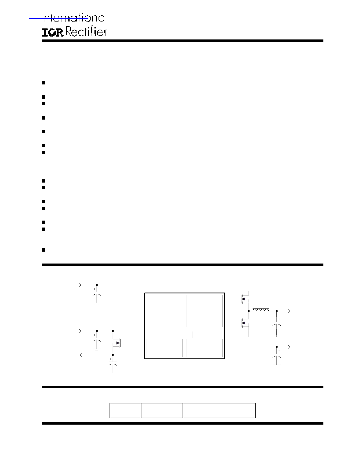
TYPICAL APPLICATION
5V
IRU3018
3.3V
LINEAR
Vout3
Figure 1 - Typical application of IRU3018.
CONTROL
PACKAGE ORDER INFORMATION
TA (!C) DEVICE PACKAGE
0 To 70 IRU3018CW 24-pin Plastic SOIC WB
Rev. 1.5
07/24/01
SWITCHER1
CONTROL
LINEAR
REGULATOR
Note: Pentium II is trademark of Intel Corp
Vout1
Vout2
3018app3-1.1
1
IRU3018
ABSOLUTE MAXIMUM RATINGS
V5 Supply Voltage .................................................... 7V
V12 Supply Voltage .................................................. 20V
Storage Temperature Range ...................................... -65°C To 150°C
Operating Junction Temperature Range ..................... 0°C To 125°C
PACKAGE INFORMATION
24-PIN WIDE BODY PLASTIC SOIC (W)
TOP VIEW
1
V12
2
VID4
3
VID3
4
VID2
5
VID1
6
VID0
7
PGood
8 17
V5
9 16
SS
10 15
Fault / Rt
11 14
Fb2
12 13
Vin2 Vout 2
24
23
22
21
20
19
18
UGate1
Phase1
LGate1
PGnd
OCSet1
Vsen1
Fb1
En
Fb3
Gate3
Gnd
θJA =80!C/W
ELECTRICAL SPECIFICATIONS
Unless otherwise specified, these specifications apply over V12=12V, V5=5V and TA=0 to 70°C. Typical values refer
to TA=25°C. Low duty cycle pulse testing is used which keeps junction and case temperatures equal to the ambient
temperature.
PARAMETER SYM TEST CONDITION MIN TYP MAX UNITS
Supply UVLO Section
UVLO Threshold-12V Supply Ramping Up 10 V
UVLO Hysteresis-12V 0.4 V
UVLO Threshold-5V Supply Ramping Up 4.3 V
UVLO Hysteresis-5V 0.3 V
Supply Current
Operating Supply Current I12 V12 6
I5 V5 20 mA
Switching Controller, Vcore (Vout 1)
VID Section
DAC Output Voltage (Note 1) VDAC 0.99Vs Vs 1.01Vs V
DAC Output Line Regulation 0.1 %
DAC Output Temp Variation 0.5 %
VID Input LO 0.8 V
VID Input HI 2 V
VID Input Internal Pull-Up 27 KΩ
Resistor to V5
Error Comparator Section
Input Bias Current 2 µA
Input Offset Voltage -2 +2 mV
Delay to Output Vdiff=10mV 100 ns
Oscillator Section (Internal)
Osc Frequency 200 KHz
2
Rev. 1.5
07/24/01
IRU3018
PARAMETER SYM TEST CONDITION MIN TYP MAX UNITS
Current Limit Section
CS Threshold Set Current 200 µA
CS Comp Offset Voltage -5 +5 mV
Hiccup Duty Cycle Css=0.1µF 10 %
Output Drivers Section
Rise Time CL=3000pF 70 ns
Fall Time CL=3000pF 70 ns
Dead Band Time Between
High Side and Synch Drive
Vcore Switcher Only CL=3000pF 200 ns
2.5V Regulator (Vout 2)
Reference Voltage Vo2 TA=25!C, Vout2=Fb2 1.260 V
Reference Voltage 1.260 V
Dropout Voltage Io=200mA 0.6 V
Load Regulation 1mA< Io <200mA 0.5 %
Line Regulation 3.1V<Vin2<4V, Vo=2.5V 0.2 %
Input Bias Current 2 µA
Output Current 200 mA
Current Limit 300 mA
Thermal Shutdown 145 !C
1.5V Regulator (Vout 3)
Reference Voltage Vo3 TA=25!C, Gate3=Fb3 1.260 V
Reference Voltage 1.260 V
Input Bias Current 2 µA
Output Drive Current 50 mA
Power Good Section
Core UV Lower Trip Point Vsen1 Ramping Down 0.90Vs V
Core UV Upper Trip Point Vsen1 Ramping Up 0.92Vs V
Core UV Hysterises 0.02Vs V
Core OV Upper Trip Point Vsen1 Ramping Up 1.10Vs V
Core OV Lower Trip Point Vsen1 Ramping Down 1.08Vs V
Core OV Hysterises 0.02Vs V
Fb2 Lower Trip Point Fb2 Ramping Down 0.95 V
Fb2 Upper Trip Point Fb2 Ramping Up 1.05 V
Fb3 Lower Trip Point Fb3 Ramping Down 0.95 V
Fb3 Upper Trip Point Fb3 Ramping Up 1.05 V
Power Good Output LO RL=3mA 0.4 V
Power Good Output HI RL=5K, Pull-Up to 5V 4.8 V
Fault (Overvoltage) Section
Core OV Upper Trip Point Vsen1 Ramping Up 1.17Vs V
Core OV Lower Trip Point Vsen1 Ramping Down 1.15Vs V
Vin2 Upper Trip Point Vin2 Ramping Up 4.3 V
Vin2 Lower Trip Point Vin2 Ramping Down 4.2 V
Fault Output HI Io=3mA 10 V
Soft-Start Section
Pull-Up Resistor to 5V OCSet=0V, Phase=5V 23 KΩ
Enable Section
En Pin Input LO Voltage Venl Regulator OFF 0.8 V
En Pin Input HI Voltage Venh Regulator ON 2 V
En Pin Input LO Current Ven=0V to 0.8V 0.01 µA
En Pin Input HI Current Ven=2V to 5V 20 µA
Note 1: Vs refers to the set point voltage given in Table 1
Rev. 1.5
07/24/01
3
IRU3018
D4
0
0
0
0
0
0
0
0
0
0
0
0
0
0
0
0
D3
D2
1
1
1
1
1
1
1
1
0
0
0
0
0
0
0
0
1
1
1
1
0
0
0
0
1
1
1
1
0
0
0
0
D1
1
1
0
0
1
1
0
0
1
1
0
0
1
1
0
0
D0
1
0
1
0
1
0
1
0
1
0
1
0
1
0
1
0
Table 1 - Set point voltage vs. VID codes
PIN DESCRIPTIONS
PIN# PIN SYMBOL PIN DESCRIPTION
1
2
3
4
5
6
7
8
9
V12
Vid4
Vid3
Vid2
Vid1
Vid0
PGood
V5
SS
This pin is connected to the 12 V supply and serves as the power Vcc pin for the output
drivers. A high frequency capacitor (typically 1µF) must be placed close to this pin and
PGnd pin and be connected directly from this pin to the ground plane for the noise free
operation.
This pin selects a range of output voltages for the DAC. When in the LOW state the range
is 1.3V to 2.05V and when it switches to HI state the range is 2.0V to 3.5V. This pin is TTL
compatible that realizes a logic “1” as either HI or Open. When left open, this pin is pulled
up internally by a 27KΩ resistor to 5V supply.
MSB input to the DAC that programs the output voltage. This pin is TTL compatible that
realizes a logic “1” as either HI or Open. When left open, this pin is pulled up internally by
a 27KΩ resistor to 5V supply.
Input to the DAC that programs the output voltage. This pin is TTL compatible that realizes
a logic “1” as either HI or Open. When left open, this pin is pulled up internally by a 27KΩ
resistor to 5V supply.
Input to the DAC that programs the output voltage. This pin is TTL compatible that realizes
a logic “1” as either HI or Open. When left open, this pin is pulled up internally by a 27KΩ
resistor to 5V supply.
LSB input to the DAC that programs the output voltage. This pin is TTL compatible that
realizes a logic “1” as either HI or Open. When left open, this pin is pulled up internally by
a 27KΩ resistor to 5V supply.
This pin is an open collector output that switches LO when any of the outputs are outside
of the specified under voltage trip point. It also switches low when Vsen1 pin is more than
10% above the DAC voltage setting.
5V supply voltage. A high frequency capacitor (0.1 to 1µF) must be placed close to this
pin and connected from this pin to the ground plane for noise free operation.
This pin provides the soft start for the switching regulator. An internal resistor charges an
external capacitor that is connected from 5V supply to this pin which ramps up the outputs of the switching regulators, preventing the outputs from overshooting as well as
limiting the input current. The second function of the Soft Start cap is to provide long off
time (HICCUP) for the synchronous MOSFET during current limiting.
Vs
1.30
1.35
1.40
1.45
1.50
1.55
1.60
1.65
1.70
1.75
1.80
1.85
1.90
1.95
2.00
2.05
D4
D3
1
1
1
1
1
1
1
1
1
1
1
1
1
1
1
1
1
1
1
1
1
1
1
1
0
0
0
0
0
0
0
0
D2
D1
1
1
1
1
0
0
0
0
1
1
1
1
0
0
0
0
1
1
0
0
1
1
0
0
1
1
0
0
1
1
0
0
D0
Vs
1
0
1
0
1
0
1
0
1
0
1
0
1
0
1
0
2.0
2.1
2.2
2.3
2.4
2.5
2.6
2.7
2.8
2.9
3.0
3.1
3.2
3.3
3.4
3.5
4
Rev. 1.5
07/24/01
PIN# PIN SYMBOL PIN DESCRIPTION
10
11
12
13
14
15
16
17
18
19
20
21
22
23
24
Fault / Rt
Fb2
Vin2
Vout2
Gnd
Gate3
Fb3
En
Fb1
Vsen1
OCSet1
PGnd
LGate1
Phase1
UGate1
This pin has dual function. It acts as an output of the OVP circuitry or it can be used to
program the frequency using an external resistor. When used as a fault detector, if the
switcher output exceed the OVP trip point, the Fault pin switches to 12V and the softstart cap is discharged. If the Fault pin is to be connected to any external circuitry, it
needs to be buffered as shown in the application circuit.
This pin provides the feedback for the internal LDO regulator which its output is Vout4.
This pin is the input that provides power for the internal LDO regulator. It is also monitored
for the under-voltage and over-voltage conditions.
This pin is the output of the internal LDO regulator.
This pin serves as the ground pin and must be connected directly to the ground plane.
This pin controls the gate of an external transistor for the 1.5V GTL+ linear regulator.
This pin provides the feedback for the linear regulator which its output drive is Gate3.
This pin is a TTL compatible Enable pin. When this pin is left open or pulled high, the
device is enabled and when it is pulled low, it will disable the switcher and the LDO
controller (Vout3) leaving the internal 200mA regulator operational. When signal is given to
enable the device, both switcher and Vout3 will go through soft-start, the same as during
start-up.
This pin provides the feedback for the synchronous switching regulator. Typically this pin
can be connected directly to the output of the switching regulator. However, a resistor
divider is recommended to be connected from this pin to Vout1 and Gnd to adjust the
output voltage for any drop in the output voltage that is caused by the trace resistance.
The value of the resistor connected from Vout1 to Fb1 must be less than 100Ω.
This pin is internally connected to the Under-voltage and over-voltage comparators sensing the Vcore status. It must be connected directly to the Vcore supply.
This pin is connected to the Drain of the power MOSFET of the Core supply and it provides
the positive sensing for the internal current sensing circuitry. An external resistor programs the CS threshold depending on the RDS of the power MOSFET. An external capacitor is placed in parallel with the programming resistor to provide high frequency noise
filtering.
This pin serves as the Power ground pin and must be connected directly to the ground
plane close to the source of the synchronous MOSFET. A high frequency capacitor (typically 1µF) must be connected from V12 pin to this pin for noise free operation.
Output driver for the synchronous power MOSFET for the Core supply.
This pin is connected to the Source of the power MOSFET for the Core supply and it
provides the negative sensing for the internal current sensing circuitry.
Output driver for the high side power MOSFET for the Core supply.
IRU3018
Rev. 1.5
07/24/01
5

IRU3018
BLOCK DIAGRAM
En
V12
V5
VID0
VID1
VID2
VID3
VID4
Vsen1
Fb3
Gate3
Vin2
Vou t2
Fb2
PGood
4.3V
17
1
8
6
5
4
3
2
19
16
15
12
13
11
7
Enable
UVLO
Vset
5Bit
DAC
V12
1.26V 0.9V
V5
1.17Vset
2.5V
1.1Vset
0.9Vset
Over
Voltage
Enable
Vset
+
Slope
Comp
Soft
Start &
Fault
Logic
Enable
Osc
PWM
Control
Over
Current
200uA
V12
V12
18
Fb1
24
UGate1
22
LGate1
23
Phase1
20
OCSet1
10
Fault / Rt
9
SS
21
PGnd
14
Gnd
6
Figure 2 - Simplified block diagram of the IRU3018.
Rev. 1.5
07/24/01

TYPICAL APPLICATION
IRU3018
12V
5V
3.3V
Vou t3
1.5V
Vou t4
2.5V
C1
C2
Q2
L1
C17
C18
C3
R5
R22
R6
R7
R8
1
V12
V5
8 23
C19
Fault/Rt
Vin2
12
U1
IRU3018
Gate3
15
Fb3
Vou t2
13
Fb2 Gnd
3018app1-1.6
1411
20
OCSet1
UGate1 24
Phase1
LGate1
PGnd
Vsen1
Fb1
En 17
PGood 7
VID0
VID1
VID2
VID3
VID4
SS
9
C9
C9
C14C10R12C8
R13
R14
22
2110
19
18
616
5
4
3
2
5V
5V
Q3
Q4 C13
R19
R15
R17
R16
R21
C15
L3
Vou t1
C16
1.8V - 3.5V
PGood
Figure 3 - Typical application of IRU3018 for an on board DC-DC converter providing power for the Vcore, GTL+ &
Clock supply for the Deschutes and the next generation processor applications.
Rev. 1.5
07/24/01
7

IRU3018
IRU3018 APPLICATION PARTS LIST
Ref Desig Description Qty Part # Manuf
Q2 MOSFET 1 IRLR024, TO-252 package IR
Q3 MOSFET 1 IRL3103S, TO-263 package IR
Q4 MOSFET with Schottky 1 IRL3103D1S, TO-263 package IR
L1 Inductor 1 L=1µH, 5052 core with 4 turns of Micro Metal
1.0mm wire
L3 Inductor 1 L=2.7µH, 5052B core with 7 turns Micro Metal
of 1.2mm wire
C1,17 Capacitor, Electrolytic 2 6MV1000GX, 1000µF, 6.3V Sanyo
C2 Capacitor, Electrolytic 1 10MV470GX, 470µF, 10V Sanyo
C3 Capacitor, Electrolytic 1 10MV1200GX, 1200µF, 10V Sanyo
C8 Capacitor, Ceramic 1 1µF, 0805
C9,15,19 Capacitor, Ceramic 3 1µF, 0603
C10 Capacitor, Ceramic 1 220pF, 0603
C13 Capacitor, Ceramic 1 1000pF, 0603
C14 Capacitor, Electrolytic 2 10MV1200GX, 1200µF, 10V Sanyo
C16 Capacitor, Electrolytic 6 6MV1500GX, 1500µF, 6.3V Sanyo
C18 Capacitor, Electrolytic 1 6MV150GX, 150µF, 6.3V Sanyo
R5 Resistor 1 19.1Ω, 1%, 0603
R6,7,8 Resistor 3 100Ω, 1%, 0603
R12 Resistor 1 3.3KΩ, 5%, 0603
R13,14,15 Resistor 3 4.7Ω, 5%, 1206
R16,17,21 Resistor 3 2.2KΩ, 1%, 0603
R22 Resistor 1 10Ω, 5%, 0603
8
Rev. 1.5
07/24/01

TYPICAL APPLICATION
(Dual Layout with HIP6018)
12V
5V
3.3V
C1
C2
L1
C3
R22
R11
1
V12
V5
8 23
(Fault)
C19
Fault/Rt
(Rt)
U1
IRU3018
Vin2
12
20
OCSet1
UGate1 24
Phase1
LGate1
PGnd
Vsen1
Fb1
En
(Comp1)
IRU3018
C14C10R12C8
R13
R14
22
2110
19
18
17
C11
Q3
Q4 C13
C12
R18
R15
R17
R16
R21
C15
R19
L3
Vou t1
C16
1.8V - 3.5V
PGood
Vou t3
1.5V
Vou t4
2.5V
Q2
C17
C18
R5
R6
R7
R8
15
13
3018app2-1.6
Gate3
Fb3
Vou t2
Fb2 Gnd
1411
C20 C9
PGood 7
VID0
VID1
VID2
VID3
VID4
SS
9
616
5
4
3
2
5V
Figure 4 - Typical application of IRU3018 in a dual layout with HIP6018 for an on-board DC-DC converter providing
power for the Vcore, GTL+ & Clock supply for the Deschutes and the next generation processor applications.
Part # R11 R18 C9 C11 C12 C19 C20
HIP6018 O V O V V O V
IRU3018 S O V O O V O
S - Short O - Open V - See IR or Harris parts list for the value
Rev. 1.5
07/24/01
Table 2 - Dual layout component table. Components that need to be modified to make
the dual layout work for IRU3018 and HIP6018.
9
IRU3018
IRU3018 APPLICATION PARTS LIST
Dual Layout with HIP6018
Ref Desig Description Qty Part # Manuf
Q2 MOSFET 1 IRLR024, TO-252 package IR
Q3 MOSFET 1 IRL3103S, TO-263 package IR
Q4 MOSFET with Schottky 1 IRL3103D1S, TO-263 package IR
L1 Inductor 1 L=1µH, 5052 core with 4 turns of Micro Metal
1.0mm wire
L3 Inductor 1 L=2.7µH, 5052B core with 7 turns of Micro Metal
1.2mm wire
C1,17 Capacitor, Electrolytic 2 6MV1000GX, 1000uF, 6.3V Sanyo
C2 Capacitor, Electrolytic 1 10MV470GX, 470µF, 10V Sanyo
C3 Capacitor, Electrolytic 1 10MV1200GX, 1200µF, 10V Sanyo
C8 Capacitor, Ceramic 1 1µF, 0805
C9,15,19 Capacitor, Ceramic 3 1µF, 0603
C10 Capacitor, Ceramic 1 220pF, 0603
C11,12,20 Capacitor, Ceramic 3 See Table 2, dual layout component
0603 × 3
C13 Capacitor, Ceramic 1 1000pF, 0603
C14 Capacitor, Electrolytic 2 10MV1200GX, 1200µF, 10V Sanyo
C16 Capacitor, Electrolytic 6 6MV1500GX, 1500µF, 6.3V Sanyo
C18 Capacitor, Electrolytic 1 6MV150GX, 150µF, 6.3V Sanyo
R5 Resistor 1 19.1Ω, 1%, 0603
R6,7,8 Resistor 3 100Ω, 1%, 0603
R11 Resistor 1 0Ω, 0603
R12 Resistor 1 3.3kΩ, 5%, 0603
R13,14,15 Resistor 3 4.7Ω, 5%, 1206
R16,17,21 Resistor 3 2.2kΩ, 1%, 0603
R18 Resistor 1 See Table 2, dual layout component
0603 × 1
R19 Resistor 1 220kΩ, 1%, 0603
R22 Resistor 1 10Ω, 5%, 0603
10
Rev. 1.5
07/24/01

APPLICATION INFORMATION
IRU3018
An example of how to calculate the components for the
application circuit is given below.
Assuming, two set of output conditions that this regulator must meet for Vcore:
a) Vo=2.8V, Io=14.2A, ∆Vo=185mV, ∆Io=14.2A
b) Vo=2V, Io=14.2A, ∆Vo=140mV, ∆Io=14.2A
The regulator design will be done such that it meets the
worst case requirement of each condition.
Output Capacitor Selection
The first step is to select the output capacitor. This is
done primarily by selecting the maximum ESR value
that meets the transient voltage budget of the total ∆Vo
specification. Assuming that the regulators DC initial
accuracy plus the output ripple is 2% of the output voltage, then the maximum ESR of the output capacitor is
calculated as:
ESR ≤ = 7mΩ
The Sanyo MVGX series is a good choice to achieve
both the price and performance goals. The 6MV1500GX,
1500µF, 6.3V has an ESR of less than 36mΩ typical.
Selecting 6 of these capacitors in parallel has an ESR
of ≈ 6mΩ which achieves our low ESR goal.
Other type of Electrolytic capacitors from other manufacturers to consider are the Panasonic FA series or the
Nichicon PL series.
Reducing the Output Capacitors Using Voltage Level
Shifting Technique
The trace resistance or an external resistor from the output
of the switching regulator to the Slot 1 can be used to
the circuit advantage and possibly reduce the number of
output capacitors, by level shifting the DC regulation point
when transitioning from light load to full load and vice
versa. To accomplish this, the output of the regulator is
typically set about half the DC drop that results from
light load to full load. For example, if the total resistance
from the output capacitors to the Slot 1 and back to the
Gnd pin of the IRU3018 is 5mΩ and if the total ∆I, the
change from light load to full load is 14A, then the output
voltage measured at the top of the resistor divider which
is also connected to the output capacitors in this case,
must be set at half of the 70mV or 35mV higher than the
DAC voltage setting. This intentional voltage level shift-
100
14.2
ing during the load transient eases the requirement for
the output capacitor ESR at the cost of load regulation.
One can show that the new ESR requirement eases up
by half the total trace resistance. For example, if the
ESR requirement of the output capacitors without voltage level shifting must be 7mΩ then after level shifting
the new ESR will only need to be 8.5mΩ if the trace
resistance is 5mΩ (7+5/2=9.5). However, one must be
careful that the combined “voltage level shifting” and the
transient response is still within the maximum tolerance
of the Intel specification. To insure this, the maximum
trace resistance must be less than:
Rs ≤ 2 × (Vspec - 0.02 × Vo - ∆Vo) / ∆I
Where:
Rs = Total maximum trace resistance allowed
Vspec = Intel total voltage spec
Vo = Output voltage
∆Vo = Output ripple voltage
∆I = load current step
For example, assuming:
Vspec = ±140mV = ±0.1V for 2V output
Vo = 2V
∆Vo = assume 10mV = 0.01V
∆I = 14.2A
Then the Rs is calculated to be:
Rs ≤ 2 ×(0.140 - 0.02 × 2 - 0.01) / 14.2 = 12.6mΩ
However, if a resistor of this value is used, the maximum
power dissipated in the trace (or if an external resistor is
being used) must also be considered. For example if
Rs=12.6mΩ, the power dissipated is:
Io2 × Rs = 14.22 × 12.6 = 2.54W
This is a lot of power to be dissipated in a system. So, if
the Rs=5mΩ, then the power dissipated is about 1W
which is much more acceptable. If level shifting is not
implemented, then the maximum output capacitor ESR
was shown previously to be 7mΩ which translated to ≈ 6
of the 1500µF, 6MV1500GX type Sanyo capacitors. With
Rs=5mΩ, the maximum ESR becomes 9.5mΩ which is
equivalent to ≈ 4 caps. Another important consideration
is that if a trace is being used to implement the resistor,
the power dissipated by the trace increases the case
temperature of the output capacitors which could seriously effect the life time of the output capacitors.
Rev. 1.5
07/24/01
11

IRU3018
Output Inductor Selection
The output inductance must be selected such that under low line and the maximum output voltage condition,
the inductor current slope times the output capacitor
ESR is ramping up faster than the capacitor voltage is
drooping during a load current step.
However, if the inductor is too small, the output ripple
current and ripple voltage become too large. One solution to bring the ripple current down is to increase the
switching frequency, however that will be at the cost of
reduced efficiency and higher system cost. The following set of formulas are derived to achieve the optimum
performance without many design iterations.
The maximum output inductance is calculated using the
following equation:
L = ESR×C×[Vin(min) - Vo(max)] / ( 2×∆I )
Where :
Vin(min) = Minimum input voltage
For Vo=2.8V, ∆I=14.2A
L = 0.006×9000×(4.75 - 2.8) / (2×14.2) = 3.7µH
Assuming that the programmed switching frequency is
set at 200KHz, an inductor is designed using the
Micrometals’ Powder Iron core material. The summary
of the design is outlined below:
The selected core material is Powder Iron, the selected
core is T50-52D from Micro Metal wound with 8 turns of
#16 AWG wire, resulting in 3µH inductance with ≈ 3mΩ
of DC resistance.
Assuming L=3µH and Fsw=200KHz (switching frequency), the inductor ripple current and the output ripple
voltage is calculated using the following set of equations:
T ≡ Switching Period
D ≡ Duty Cycle
Vsw ≡ High-side MOSFET ON Voltage
RDS ≡ MOSFET On-resistance
Vsync ≡ Synchronous MOSFET ON Voltage
∆Ir ≡ Inductor Ripple Current
∆Vo ≡Output Ripple Voltage
T = 1 / Fsw
Vsw = Vsync = Io × RDS
D ≈ (Vo + Vsync) / (Vin - Vsw + Vsync)
Ton = D × T
Toff = T - Ton
∆Ir = (Vo + Vsync) × Tof f / L
∆Vo = ∆Ir × ESR
In our example for Vo=2.8V and 14.2 A load, assuming
IRL3103 MOSFET for both switches with maximum on
resistance of 19mΩ, we have:
T = 1 / 200000 = 5µs
Vsw = Vsync = 14.2 × 0.019 = 0.27V
D ≈ (2.8 + 0.27) / (5 - 0.27 + 0.27) = 0.61
Ton = 0.61 × 5 = 3.1µs
To ff = 5 - 3.1 = 1.9µs
∆Ir = (2.8 + 0.27) × 1.9 / 3 = 1.94A
∆Vo = 1.94 × 0.006 = 0.011V = 11mV
Power Component Selection
Assuming IRL3103 MOSFETs as power components,
we will calculate the maximum power dissipation as follows:
For high-side switch the maximum power dissipation
happens at maximum Vo and maximum duty cycle.
Dmax ≈ (2.8 + 0.27) / (4.75 - 0.27 + 0.27) = 0.65
PDH = Dmax × Io2 × RDS(max)
PDH = 0.65 × 14.22 × 0.029 = 3.8W
RDS(max) = Maximum RDS(on) of the MOSFET at 125!C
For synch MOSFET, maximum power dissipation happens at minimum Vo and minimum duty cycle.
Dmin ≈ (2 + 0.27) / (5.25 - 0.27 + 0.27) = 0.43
PDS = (1-Dmin) × Io2 × RDS(max)
PDS = (1 - 0.43) × 14.22 × 0.029 = 3.33 W
Heat Sink Selection
Selection of the heat sink is based on the maximum
allowable junction temperature of the MOSFETS. Since
we previously selected the maximum RDS(on) at 125!C,
then we must keep the junction below this temperature.
Selecting TO-220 package gives θJC=1.8!C/W (from the
venders’ data sheet) and assuming that the selected
heat sink is black anodized, the heat-sink-to-case thermal resistance is: θcs=0.05!C/W, the maximum heat
sink temperature is then calculated as:
Ts = TJ - PD × (θJC + θcs)
Ts = 125 - 3.82 × (1.8 + 0.05) = 118!C
With the maximum heat sink temperature calculated in
the previous step, the heat-sink-to-air thermal resistance
(θSA) is calculated as follows:
Assuming TA = 35!C:
∆T = Ts - TA = 118 - 35 = 83!C
Temperature Rise Above Ambient
θSA = ∆T / PD = 83 / 3.82 = 22!C/W
12
Rev. 1.5
07/24/01

IRU3018
Next, a heat sink with lower θSA than the one calculated
in the previous step must be selected. One way to do
this is to look at the graphs of the “Heat Sink Temp Rise
Above the Ambient” vs. the “Power Dissipation” given in
the heat sink manufacturers’ catalog and select a heat
sink that results in lower temperature rise than the one
calculated in previous step. The following heat sinks from
AAVID and Thermalloy meet this criteria.
Co. Part #
Thermalloy............................6078B
AAVID..................................577002
Following the same procedure for the Schottky diode
results in a heat sink with θSA=25!C/W. Although it is
possible to select a slightly smaller heat sink, for simplicity the same heat sink as the one for the high side
MOSFET is also selected for the synchronous MOSFET.
Switcher Current Limit Protection
The IRU3018 uses the MOSFET R
resistor to sense the MOSFET current and compares to
a programmed voltage which is set externally via a resistor (Rcs) placed between the drain of the MOSFET
and the “OCSet1” terminal of the IC as shown in the
application circuit. For example, if the desired current
limit point is set to be 22A, for the synchronous and 16A
for the non-synchronous, and from our previous selection, the maximum MOSFET RDS(on)=19mΩ, then the current sense resistor Rcs is calculated as:
Vcs = ICL × RDS = 22 × 0.019 = 0.418V
Rcs = Vcs / IB = (0.418V) / (200µA) = 2.1KΩ
Where:
IB = 200µA is the internal current setting of the
IRU3018
Switcher Frequency Selection
The IRU3018 frequency is internally set at 200KHz with
no external timing resistor. However, it can be adjusted
up by using an external resistor from Rt pin to Gnd or
can be adjusted down if the resistor is connected to the
12V supply.
1.5V, GTL+ Supply LDO Power MOSFET Selection
The first step in selecting the power MOSFET for the
1.5V linear regulator is to select its maximum RDS(on) of
the pass transistor based on the input to output Dropout
voltage and the maximum load current.
RDS(max) = (Vin - Vo) / IL
For Vo = 1.5V, Vin = 3.3V and, IL = 2A
RDS(max) = (3.3 - 1.5) / 2 = 0.9Ω
DS(on) as the sensing
Note that since the MOSFETs R
perature, this number must be divided by ≈ 1.5, in order
to find the RDS(on) max at room temperature. The Motorola
MTP3055VL has a maximum of 0.18Ω RDS(on) at room
temperature, which meets our requirement.
To select the heat sink for the LDO MOSFET, first calculate the maximum power dissipation of the device
and then follow the same procedure as for the switcher.
PD = (Vin - Vo) × IL
Where:
PD = Power Dissipation of the Linear Regulator
IL = Linear Regulator Load Current
For the 1.5V and 2A load:
PD = (3.3 - 1.5) × 2 = 3.6W
Assuming T
Ts = T J - PD × (θJC + θcs)
Ts = 125 - 3.6 × (1.8 + 0.05) = 118!C
With the maximum heat sink temperature calculated in
the previous step, the heat-sink-to-air thermal resistance
(θSA) is calculated as follows:
Assuming TA = 35°C:
∆T = Ts - Ta = 118 - 35 = 83 °C
Temperature Rise Above Ambient
θSA = ∆T / PD = 83 / 3.6 = 23!C/W
The same heat sink as the one selected for the switcher
MOSFETs is also suitable for the 1.5V regulator.
2.5V, Clock Supply
The IRU3018 provides an internal ultra low dropout regulator with a minimum of 200mA current capability that
converts 3.3V supply to a programmable regulated 2.5V
supply to power the clock chip. The internal regulator
has short circuit protection with internal thermal shutdown.
1.5V and 2.5V Supply Resistor Divider Selection
Since the internal voltage reference for the linear regulators is set at 1.26V for IRU3018, there is a need to use
external resistor dividers to step up the voltage. The resistor dividers are selected using the following equations:
Vo = (1 + Rt/RB) × Vref
Where:
Rt = Top resistor divider
RB = Bottom resistor divider
Vref = 1.26V typical
J(max) = 125!C:
DS(on) increases with tem-
Rev. 1.5
07/24/01
13

IRU3018
For 1.5V supply
Assuming RB=100Ω:
Rt = RB × [(Vo/Vref) - 1]
Rt = 100 × [(1.5/1.26) - 1] = 19.1Ω
For 2.5V supply
Assuming RB=200Ω:
Rt = R
B × [(Vo/Vref) - 1]
Rt = 200 × [(2.5/1.26) - 1] = 197Ω
Select Rt=200Ω
Switcher Output Voltage Adjust
As it was discussed earlier, the trace resistance from
the output of the switching regulator to the Slot 1 can be
used to the circuit advantage and possibly reduce the
number of output capacitors, by level shifting the DC
regulation point when transitioning from light load to full
load and vice versa. To account for the DC drop, the
output of the regulator is typically set about half the DC
drop that results from light load to full load. For example,
if the total resistance from the output capacitors to the
Slot 1 and back to the Gnd pin of the IRU3018 is 5mΩ
and if the total ∆I, the change from light load to full load
is 14A, then the output voltage measured at the top of
the resistor divider which is also connected to the output capacitors in this case, must be set at half of the
70mV or 35mV higher than the DAC voltage setting. To
do this, the top resistor of the resistor divider (R17 in the
application circuit) is set at 100Ω, and the R19 is calculated. For example, if DAC voltage setting is for 2.8V
and the desired output under light load is 2.835V, then
R19 is calculated using the following formula:
R19 = 100×[VDAC/(Vo - 1.004×VDAC)] (Ω)
R19 = 100×[2.8/(2.835 - 1.004×2.800)] = 11.76KΩ
Select 11.8KΩ, 1%
Note: The value of the top resistor must not exceed 100Ω.
The bottom resistor can then be adjusted to raise the
output voltage.
cap thereby limiting the input current. For example, with
1µF of soft-start capacitor, the ramp up rate is approximated to be 1V/20ms. For example if the output capacitance is 9000µF, the maximum start up current will be:
I = 9000µF × (1V/20ms) = 0.45A
The other function of the soft-start cap is to provide an
off time between the current limit cycles(HICCUP) in order for the synchronous MOSFET to cool off and survive
the short circuit condition. The off time between the current limit cycles is approximated as:
THICCUP = 60×Css (ms)
For example if Css=1µF, T HICCUP = 60×1 = 60ms
Input Filter
It is recommended to place an inductor between the
system 5V supply and the input capacitors of the switching regulator to isolate the 5V supply from the switching
noise that occurs during the turn on and off of the switching components. Typically an inductor in the range of 1
to 3µH will be sufficient in this type of application.
External Shutdown
The best way to shutdown the IRU3018 is to pull down
on the soft-start pin using an external small signal transistor such as 2N3904 or 2N7002 small signal MOSFET.
This allows slow ramp up of the output, the same as the
power up.
Layout Considerations
Switching regulators require careful attention to the layout of the components, specifically power components
since they switch large currents. These switching components can create large amount of voltage spikes and
high frequency harmonics if some of the critical components are far away from each other and are connected
with inductive traces. The following is a guideline of how
to place the critical components and the connections
between them in order to minimize the above issues.
Start the layout by first placing the power components:
Soft-Start Capacitor Selection
The soft-start capacitor must be selected such that during the start-up when the output capacitors are charging
up, the peak inductor current does not reach the current
limit threshold. A minimum of 1µF capacitor insures this
for most applications. An internal resistor charges the
soft-start capacitor which slowly ramps up the inverting
input of the PWM comparator Vfb3. This insures the
output voltage to ramp at the same rate as the soft-start
14
1) Place the input capacitor C14 and the high-side
MOSFET, Q3 as close to each other as possible.
2) Place the synchronous MOSFET, Q4 and the Q3 as
close to each other as possible with the intention
that the source of Q3 and drain of the Q4 has the
shortest length.
3) Place the snubber R15 & C13 between Q4 & Q3.
Rev. 1.5
07/24/01

IRU3018
4) Place the output inductor, L3 and the output capacitors, C16 between the mosfet and the load with output capacitors distributed along the slot 1 and close
to it.
5) Place the bypass capacitors, C8 and C19 right next
to 12V and 5V pins. C8 next to the 12V, pin 1 and
C19 next to the 5V, pin 8.
6) Place the IRU3018 such that the PWM output drives,
pins 24 and 22 are relatively short distance from gates
of Q3 and Q4.
7) Place all resistor dividers close to their respective
feedback pins.
8) Place the 2.5V output capacitor, C18 close to the pin
13 of the IC and the 1.5V output capacitor, C17 close
to the Q2 MOSFET.
Note: It is better to place the 1.5V linear regulator
components close to the 3018 and then run a trace
from the output of the regulator to the load. However,
if this is not possible then the trace from the linear
drive output pin, pin 16 must be run away from any
high frequency data signals.
It is critical, to place high frequency ceramic capacitors close to the clock chip and termination resistors
to provide local bypassing.
9) Place R12 and C10 close to pin 20
Component connections:
Note: It is extremely important that no data bus should
be passing through the switching regulator section specifically close to the fast transition nodes such as PWM
drives or the inductor voltage.
Using the 4 layer board, dedicate on layer to ground,
another layer as the power layer for the 5V, 3.3V, Vcore,
1.5V and if it is possible for the 2.5V.
Connect all grounds to the ground plane using direct
vias to the ground plane.
Use large low inductance/low impedance plane to connect the following connections either using component
side or the solder side.
a) C14 to Q3 Drain
b) Q3 Source to Q4 Drain
c) Q4 drain to L3
d) L3 to the output capacitors, C16
e) C16 to the load, slot 1
f) Input filter L1 to the C16 and C3
g) C1 to Q2 drain
h) C17 to the Q2 source
I) A minimum of 0.2 inch width trace from the C18
capacitor to pin 13
Connect the rest of the components using the shortest
connection possible.
10) Place C9 close to pin 9
Rev. 1.5
07/24/01
15

IRU3018
IRU3018 APPLICATION PARTS LIST
Dual Layout with HIP6016
Ref Desig Description Qty Part # Manuf
Q3,4 MOSFET 2 IRL3103
IRL3103S (Note 1) IR
Q5 MOSFET, GP 1 2N7002 Motorola
Q2 MOSFET 1 MTP3055VL, TO-263 package Motorola
L1 Inductor 1 L=1µH Micro Metal
L3 Inductor 1 Core: L=2µH, R=2mΩ Micro Metal
C16 Capacitor, Electrolytic 6 6MV1500GX, 1500µF, 6.3V, Sanyo
C14 Capacitor, Electrolytic 2 6MV1500GX, 1500µF, 6.3V, Sanyo
C3 Capacitor, Electrolytic 1 6MV1500GX, 1500µF, 6.3V, Sanyo
C18 Capacitor, Electrolytic 1 220µF, 6.3V, ECAOJFQ221 Panasonic
C17,C1 Capacitor, Electrolytic 2 680µF, 10V, EEUFA1A681L Panasonic
C2 Capacitor, Electrolytic 1 680µF, 10V, EEUFA1A681L Panasonic
C8,19 Capacitor, Ceramic 2 0805Z105P250NT Novacap
1µF, 25V, Z5U, 0805 SMT
C9 Capacitor , Ceramic 1 0805Z105P250NT Novacap
1µF, 25V, Z5U, 0805 SMT
See Table 2, Dual layout component
C10 Capacitor, Ceramic 1 220pF, SMT 0805 size
C13 Capacitor, Ceramic 1 470pF, SMT 0805 size
C9,11, See Table 2, Dual layout component
12,15,20
R12 Resistor 1 2.21KΩ, 1%, SMT 0805 size
R13,14 Resistor 2 10Ω, 5%, SMT 1206 size
R15 Resistor 1 10Ω, 5%, SMT 1206 size
R20 Resistor 1 10kΩ, 5%, SMT 0805 size
R6 Resistor 1 100Ω, 1%, SMT 0805 size
R8 Resistor 1 200Ω, 1%, SMT 0805 size
R5 Resistor 1 19.1Ω, 1%, SMT 0805 size
R7 Resistor 1 200Ω, 1%, SMT 0805 size
R17 Resistor 1 100Ω, 1%, SMT 0805 size
R19 Resistor 1 10kΩ, 1%, SMT 0805 size
HS3,4 Q1,3,4 Heatsink 2 6270 Thermalloy
R11,16,18, 21, 22 See Table 2, Dual layout component
Note 1: For the applications where it is desirable not to use the Heat sink, the IRL3103S MOSFET in the
TO-263 SMT package with 1" square of pad area using top and bottom layers of the board as a minimum
is required.
16
IR WORLD HEADQUARTERS : 233 Kansas St., El Segundo, California 90245, USA Tel: (310) 252-7105
TAC Fax: (310) 252-7903
Visit us at www.irf.com for sales contact information.
Data and specifications subject to change without notice. 02/01
Rev. 1.5
07/24/01
 Loading...