IOR IRSF3031 User Manual

查询IRSF3031供应商
Provisional Data Sheet No. PD 6.069A
IRSF3031
FULLY PROTECTED DMOS POWER SWITCH
Features
■ Extremely Rugged for Harsh Operating Environments
■ Over Temperature Protection
■ Over Current Protection
■ Active Drain-to-Source Clamp
■ ESD Protection
■ Compatible with Standard Power MOSFET
■ Low Operating Input Current
■ Monolithic Construction
■ Dual Set/Reset Threshold Input
Description
The IRSF3031 is a three-terminal monolithic SMART POWER MOSFET with built-in short circuit, over-temperature, ESD and over-voltage
protections and dual set/reset threshold input.
The on-chip protection circuit latches off the power MOSFET in case
the drain current exceeds 4A (typical) or the junction temperature exceeds 165°C (typical) and keeps it off until the input is driven below the
Reset Threshold voltage. The drain-to-source voltage is actively
clamped at 55V (typical) prior to the avalanche of the power MOSFET,
thus improving its performance during turn-off with inductive loads.
The input requirements are very low (100µA typical) which makes the
IRSF3031 compatible with most existing designs based on standard
power MOSFETs.
Absolute Maximum Ratings
Absolute Maximum Ratings indicate sustained limits beyond which damage to the device may occur. (Tc = 25°C unless
otherwise specified.)
V
ds(clamp)
R
ds(on)
I
ds(sd)
T
j(sd)
E
AS
Applications
■ Solenoid Driver
■ DC Motor Driver
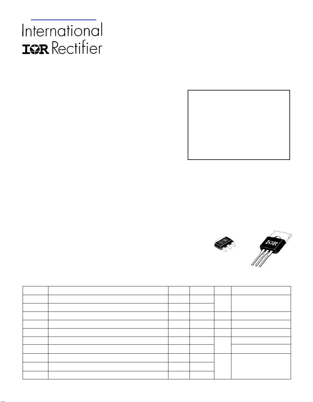
Available Packages
IRSF3031
(TO-220AB)
IRSF3031L
(SOT-223)
50 V
200 m
1.8 A
o
165
200 mJ
Ω
C
V
ds, max
V
in, max
I
ds
P
d
E
AS
V
esd1
V
esd2
T
Jop
T
Stg
T
L
Minimum Maximum Units Test Conditions
Continuous Drain to Source Voltage 50
Continuous Input Voltage 0 8
Continuous Drain Current self limited
Power Dissipation 30 W T
Unclamped Single Pulse Inductive Energy 200 mJ
Electrostatic Discharge Voltage (Human Body Model) 4000
Electrostatic Discharge Voltage (Machine Model) 1000 200pF, 0Ω
Operating Junction Temperature Range -40 150
Storage Temperature Range -40 150 °C
Lead Temperature (Soldering, 10 seconds) 300
V
V
≤ 25°C
c
1000pF. 1.5kΩ

IRSF3031
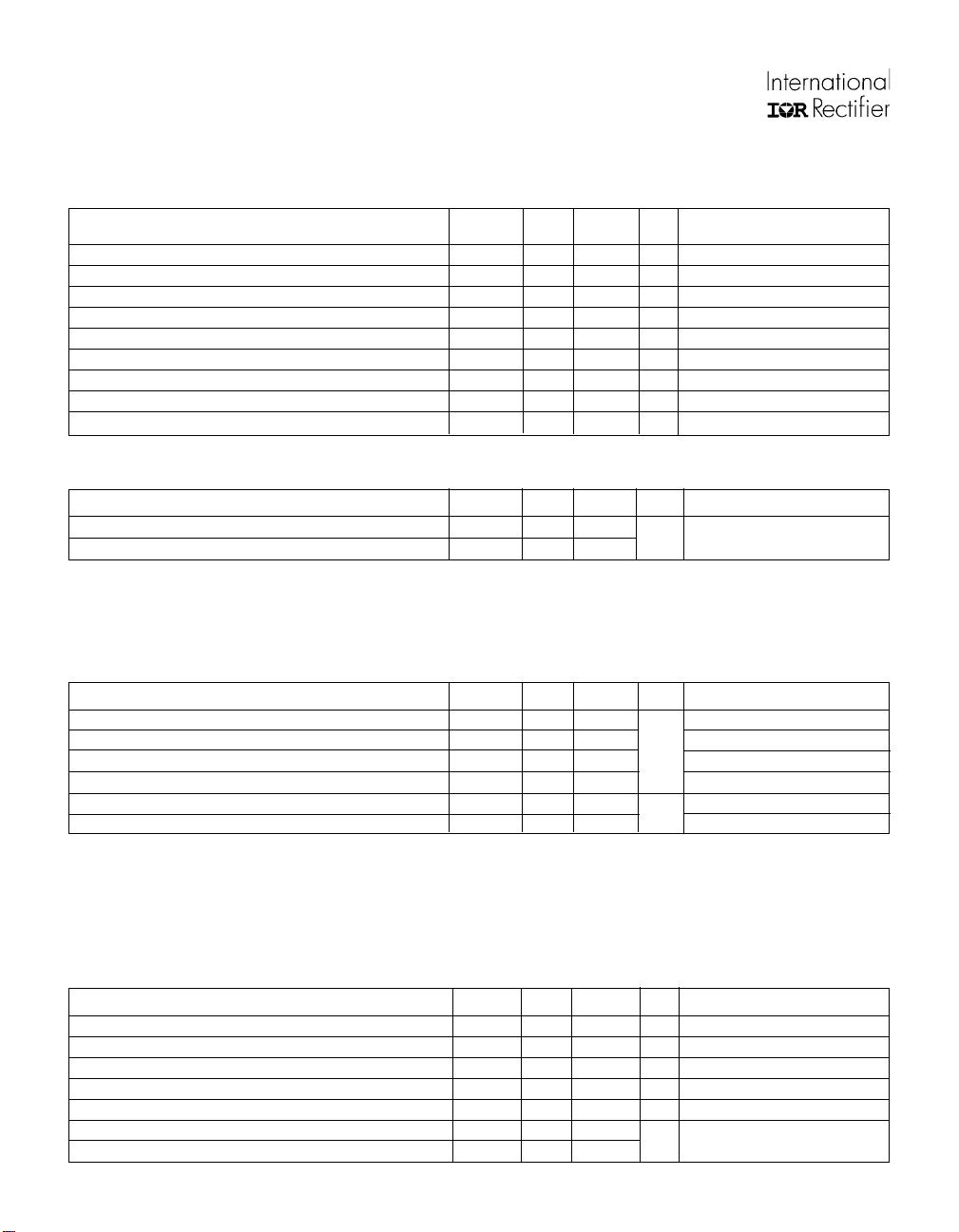
Static Electrical Characteristics
(Tc = 25°C unless otherwise specified.)
Minimum Typical Maximum Units Test Conditions
V
ds,clamp
R
ds(on)
I
dss
V
set
V
reset
I
i,on
I
i,off
V
in, clamp
V
sd
Thermal Characteristics
RΘ
RΘ
Switching ElectricalCharacteristics
(VCC = 14V, Resistive Load (RL) = 10Ω, Rin= 100Ω. Typical specifications measured at TC= 25°C. Min/max specifications are for T
t
don
t
r
t
doff
t
f
SR Output Positive Slew Rate -5 5
SR Output Positive Slew Rate -5 5 Vin = 2V to 5V, -dVds/dt
Drain to Source Clamp Voltage 50 56 65 V Ids = 2A
Drain to Source On Resistance 155 200 mΩ V
= 5V, Ids = 2A
in
Drain to Source Leakage Current 250 µA Vds = 40V, Vin = 0V
Input Threshold Voltage 2.5 3.2 4.0 V V
Input Protection Reset Threshold Voltage 0.5 1.0 1.5 V V
= 5V, Ids > 10mA
ds
= 5V, Ids < 10µA
ds
Input Supply Current (Normal Operation) 100 300 µA Vin = 5V
Input Supply Current (Protection Mode) 120 400 µA Vin = 5V
Input Clamp Voltage 9 10 V Iin = 10mA
Body-Drain Diode Forward Drop 1.5 V Ids = -2A, R
= 1kΩ
in
Minimum Typical Maximum Units Test Conditions
Thermal Resistance, Junction-to-Case 4
jc
Thermal Resistance, Junction-to-Ambient 62
jA
= -40°C to TC=125°C unless otherwise specified.)
C
°C/W
Minimum Typical Maximum Units Test Conditions
Turn-On Delay Time 30 Vin = 2V to 5V, 50% to 90%
Rise Time 30
Turn-Off Delay Time 30 Vin = 2V to 5V, 50% to 10%
Fall Time 30 Vin = 2V to 5V, 10% to 90%
Vin = 2V to 5V, 90% to 10%
µs
Vin = 2V to 5V, +dVds/dt
V/µs
Protection Characteristics
(TC= 25 °C unless otherwise specified. Min/Max specifications are for TC= -40°C to TC = +125°C unless otherwise
specified.)
Minimum Typical Maximum Units Test Conditions
I
ds(sd)
T
j(sd)
V
protect
t
Iresp
I
peak
t
reset
t
Tresp
Current Limit 1.8 4 6 A Vin = 5V
Over Temperature Shutdown Threshold 155 165 °C Vin = 5V, Ids = 2A
Min. Input Voltage for Over-temp function 3 V
Over Current Response Time TBD µs
Peak Short Circuit Current TBD A
Protection Reset Time TBD
µs
Over-Temperature Response Time TBD
 Loading...