IOR IRS20124S-PbF User Manual
查询IRS20124S供应商
DIGITAL AUDIO DRIVER WITH DISCRETE DEAD-TIME AND PROTECTION
Data Sheet No. PD60240 revA
IRS20124S(PbF)
Features
• 200V high voltage ratings deliver up to 1000W
output power in Class D audio amplifier
applications
• Integrated dead-time generation and bi-directional
over current sensing simplify design
• Programmable compensated preset dead-time for
improved THD performances over temperature
• High noise immunity
• Shutdown function protects devices from overload
conditions
• Operates up to 1MHz
• 3.3V/5V logic compatible input
Typical Application Diagram
Product Summary
V
SUPPLY
IO+/- 1A / 1.2A typ.
Selectable Dead Time
Prop Delay Time 70ns typ.
Bi-directional Over
Current Sensing
200V max.
15/25/35/45ns typ.
Package
<20V
<200V
14-Lead SOIC
IN
<20V
OC
SD
www.irf.com 1
IN
OCSET1
DT/SD
OCSET2
OC
COM
LO
IRS20124
V
NC
NC
VB
HO
VS
NC
CC
IRS20124S(PbF)
Description
The IRS20124S is a high voltage, high speed power MOSFET driver with internal dead-time and shutdown
functions specially designed for Class D audio amplifier applications.
The internal dead time generation block provides accurate gate switch timing and enables tight dead-time
settings for better THD performances.
In order to maximize other audio performance characteristics, all switching times are designed for immunity
from external disturbances such as VCC perturbation and incoming switching noise on the DT pin. Logic
inputs are compatible with LSTTL output or standard CMOS down to 3.0V without speed degradation. The
output drivers feature high current buffers capable of sourcing 1.0A and sinking 1.2A. Internal delays are
optimized to achieve minimal dead-time variations. Proprietary HVIC and latch immune CMOS technologies
guarantee operation down to Vs= –4V, providing outstanding capabilities of latch and surge immunities with
rugged monolithic construction.
Absolute Maximum Ratings
Absolute maximum ratings indicate sustained limits beyond which damage to the device may occur. All voltage parameters
are absolute voltages referenced to COM. All currents are defined positive into any lead. The thermal resistance and power
dissipation ratings are measured under board mounted and still air conditions.
Symbol Definition Min. Max. Units
V
B
V
s
V
HO
V
CC
V
LO
V
IN
V
OC
V
OCSET1
V
OCSET2
dVs/dt Allowable Vs voltage slew rate - 50 V/ns
Pd Maximum power dissipation - 1.25 W
Rth
JA
T
J
T
S
T
L
2 www.irf.com
High side floating supply voltage -0.3 220 V
High side floating supply voltage VB-20 VB+0.3 V
High side floating output voltage Vs-0.3 VB+0.3 V
Low side fixed supply voltage -0.3 20 V
Low side output voltage -0.3 Vcc+0.3 V
Input voltage -0.3 Vcc+0.3 V
OC pin input voltage -0.3 Vcc+0.3 V
OCSET1 pin input voltage -0.3 Vcc+0.3 V
OCSET2 pin input voltage -0.3 Vcc+0.3 V
Thermal resistance, Junction to ambient - 100 °C/W
Junction Temperature - 150 °C
Storage Temperature -55 150 °C
Lead temperature (Soldering, 10 seconds) - 300 °C
IRS20124S(PbF)
Recommended Operating Conditions
For Proper operation, the device should be used within the recommended conditions. The Vs and COM
offset ratings are tested with all supplies biased at 15V differential.
Symbol Definition Min. Max. Units
V
B
V
S
V
HO
V
CC
V
LO
V
IN
V
OC
V
OCSET1
V
OCSET2
T
A
Note 1: Logic operational for VS equal to -8V to 200V. Logic state held for VS equal to -8V to -VBS.
Dynamic Electrical Characteristics
V
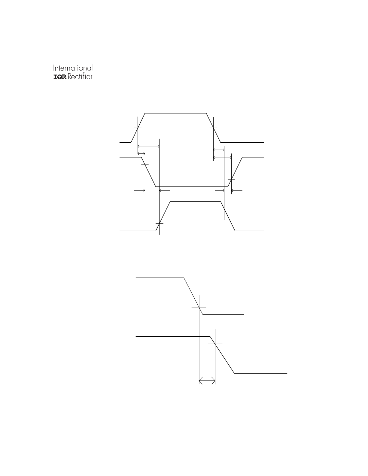
(VCC, VBS) = 15V, CL = 1nF and TA = 25°C unless otherwise specified. Figure 2 shows the timing definitions.
BIAS
High side floating supply absolute voltage Vs+10 Vs+18 V
High side floating supply offset voltage Note 1 200 V
High side floating output voltage Vs V
B
Low side fixed supply voltage 10 1 8 V
Low side output voltage 0 VCC V
Logic input voltage 0 VCC V
OC pin input voltage 0 VCC V
OCSET1 pin input voltage 0 VCC V
OCSET2 pin input voltage 0 VCC V
Ambient Temperature -40 125 °C
V
Symbol Definition Min. Typ. Max. Units Test Conditions
t
on
t
off
t
t
tsd Shutdown propagation delay — 140 200
toc Propagation delay time from Vs>Vsoc+ to OC — 2 8 0 — OC
twoc min OC pulse width — 100 —
toc filt OC input filter time — 200 —
DT1 Deadtime: LO turn-off to HO turn-on (DT
DT2 Deadtime: LO turn-off to HO turn-on (DT
DT3 Deadtime: LO turn-off to HO turn-on (DT
DT4 Deadtime: LO turn-off to HO turn-on (DT
& HO turn-off to LO turn-on (DT
www.irf.com 3
High & low side turn-on propagation delay — 60 80
High & low side turn-off propagation delay — 60 80
Turn-on rise time — 25 40
r
Turn-off fall time — 15 35
f
)
LO-HO
& HO turn-off to LO turn-on (DT
& HO turn-off to LO turn-on (DT
& HO turn-off to LO turn-on (DT
) 0 15 40 VDT>V
HO-LO
)
LO-HO
) 5 2 5 50 V
HO-LO
)
LO-HO
) 10 35 60 V
HO-LO
)
LO-HO
T= V
HO-LO)VD
15 45 70 V
DT4
nsec
VS=0V
VS=200V
SET1
OC
SET2
DT1>VDT
DT2>VDT
DT3>VDT
=3.22V
=1.20V
DT1
> V
DT2
> V
DT3
> V
DT4
IRS20124S(PbF)
Static Electrical Characteristics
V
(VCC, VBS) = 15V and TA = 25°C unless otherwise specified.
BIAS
Symbol Definition Min. Typ. Max. Units Test Conditions
UV
UV
UV
UV
V
V
V
V
V
OH
V
OL
I
QBS
I
QCC
I
LK
I
IN+
I
IN-
I
o+
I
o-
V
DT1
V
DT2
V
DT3
V
DT4
SOC+
SOC-
Logic high input voltage 2.5 — — Vcc=10~20V
IH
Logic low input voltage — — 1.2
IL
High level output voltage, V
Low level output voltage, V
Vcc supply UVLO positive threshold 8.3 9.0 9.7
CC+
Vcc supply UVLO negative threshold 7.5 8.2 8.9
CC-
High side well UVLO positive threshold 8.3 9.0 9.7
BS+
High side well UVLO negative threshold 7.5 8.2 8.9
BS-
High side quiescent current — — 1
Low side quiescent current — — 4 VDT =V
BIAS
O
– V
— — 1.2 Io=0A
O
— — 0.1 Io=0A
V
mA
High to Low side leakage current — — 50 VB=VS =200V
Logic “1” input bias current — 3 10 VIN =3.3V
µA
Logic “0” input bias current — 0 1.0 VIN =0V
Output high short circuit current (Source) — 1. 0 — Vo=0V, PW<10µS
Output low short circuit current (Sink) — 1.2 — Vo=15V, PW<10µS
A
DT mode select threshold 1 0.8xVcc 0.89xVcc 0.97xVcc
DT mode select threshold 2 0.51xVcc 0.57xVcc 0.63xVcc
DT mode select threshold 3 0.32xVcc 0.36xVcc 0.40xVcc
DT mode select threshold 4 0.21xVcc 0.23xVcc 0.25xVcc
Positive OC threshold in Vs 0.75 1.0 1.25 OC
V
OC
Negative OC threshold in Vs -1.25 -1.0 -0.75 OC
OC
SET1
SET
SET1
SET2
cc
=3.22V
2=1.20
=3.22V
=1.20V
4 www.irf.com
IRS20124S(PbF)
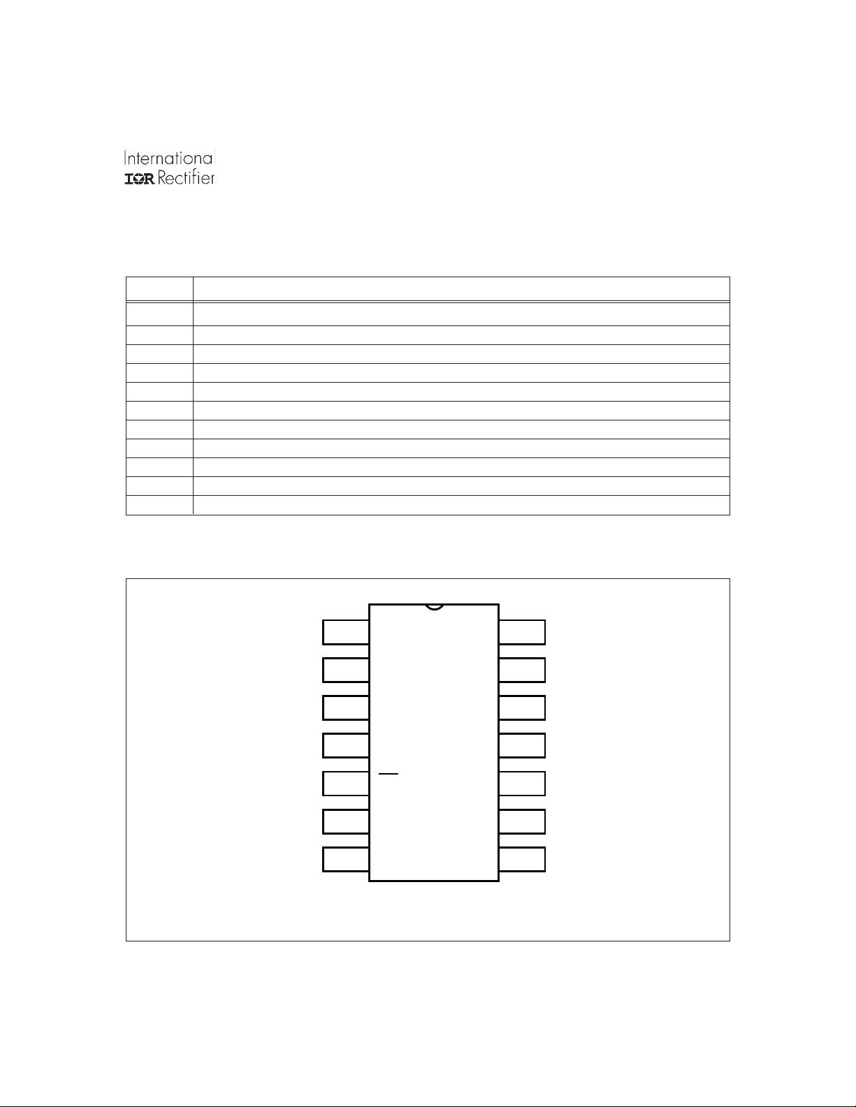
Lead Definitions
Symbol Description
VCC Low side logic Supply voltage
VB High side floating supply
HO High side output
VS High side floating supply return
IN Logic input for high and low side gate driver outputs (HO and LO), in phase with HO
DT/SD Input for programmable dead-time, referenced to COM. Shutdown LO and HO when tied to COM
COM Low side supply return
LO Low side output
OC Over current output (negative logic)
OC
OC
SET1
SET2
Input for setting negative over current threshold
Input for setting positive over current threshold
VB
VS
CC
14
13
12
11
10
9
8
1
IN
2
OCSET1
3
DT/SD
OCSET2
4
5
OC
6
COM
7
LO
IR20124S 14 Lead SOIC (narrow body)
www.irf.com 5
NC
NC
HO
NC
V
IRS20124S(PbF)
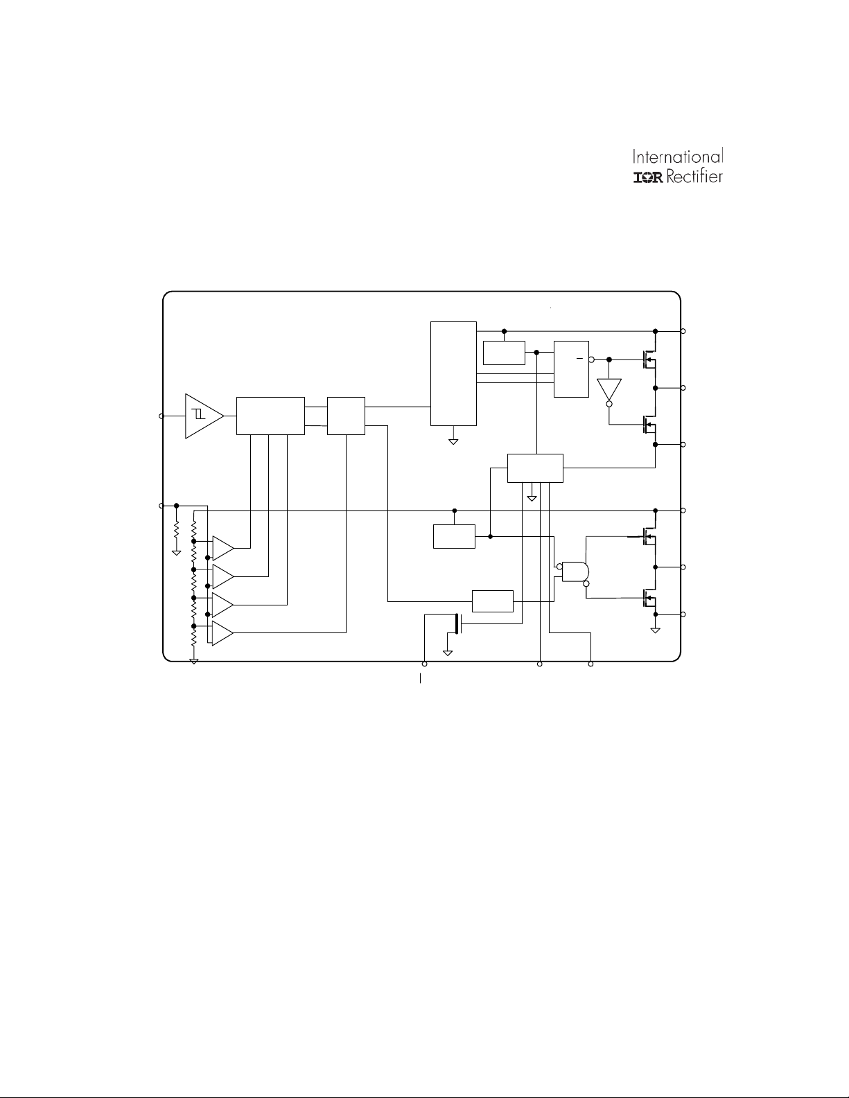
Block Diagram
DT/SD
UV
UV
DETECT
DELAY
CURRENT
SENSIN G
LEVEL
SHIFTER
IN
DEAD
TIME
SD
DETECT
OC
UV
Q
S
R
2
T
E
S
OCSET1
C
O
VB
HO
VS
Vcc
LO
COM
6 www.irf.com
IRS20124S(PbF)
IN
HO
LO
50% 50%
t
on(L)
t
off(H)
90%
DT
HO-LO
10%
Figure 1. Switching Time Waveform Definitions
DT/SD
t
t
on(H)
off(L)
DT
10%
LO-HO
90%
V
SD
HO
LO
T
SD
90%
Figure 2. Shutdown Waveform Definitions
www.irf.com 7
IRS20124S(PbF)
LO
COM
toc filt
VS
V
soct
COM
HIGH
OC
COM
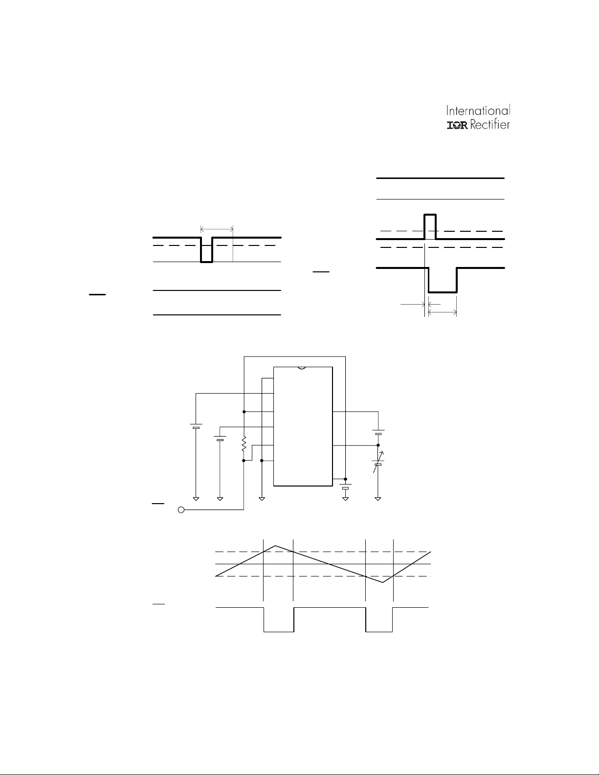
Figure 3. OC Input FilterTime Definitions
10k
IN
OCSET1
DT/SD
OCSET2
__
OC
COM
LO
VS
OC
NC
NC
VB
HO
VS
NC
CC
V
Soc+
V
COM
V
Soc-
tdoc
twoc
Figure 4. OC Waveform Definitions
15V
Vsoc+
Vsoc-
15V
OC
Vsoc+
VS
COM
Vsoc-
OC
Figure 5. OC Waveform Definitions
8 www.irf.com
 Loading...