查询IRG4CC40UB供应商
IRG4CC40UB IGBT Die in Wafer Form
Electrical Characteristics ( Wafer Form )
Parameter Description Guaranteed (Min/Max) Test Conditions
V
CE (on)
V
(BR)CES
V
GE(th)
I
CES
I
GES
Mechanical Data
Norminal Backmetal Composition, Thickness: Cr-Ni / V-Ag ( 1kA-2kA-2.5kA )
Norminal Front Metal Composition, Thickness: 99% Al, 1% Si (4 microns)
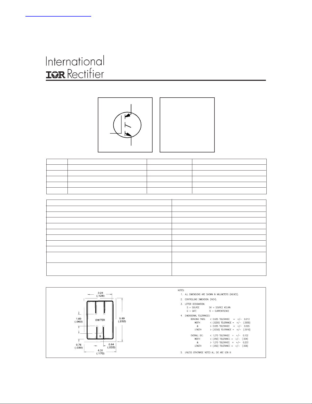
Dimensions: 0.170" x 0.232"
Wafer Diameter: 150mm, with std. < 100 > flat
Wafer thickness: .015" + / -.003"
Relevant Die Mechanical Dwg. Number 01-5219
Minimum Street Width 100 Microns
Reject Ink Dot Size 0.25mm Diameter Minimum
Ink Dot Location Consistent throughout same wafer lot
Recommended Storage Environment: Store in original container, in dessicated
Recommended Die Attach Conditions For optimum electrical results, die attach
Reference Standard IR packaged part ( for design ) : IRG4PC40U
Die Outline
Collector-to-Emitter Saturation Voltage 4.5V Max. IC = 10A, TJ = 25°C, VGE = 15V
Colletor-to-Emitter Breakdown Voltage 600V Min. TJ = 25°C, I
Gate Threshold Voltage 3.0V Min.,6.0V Max. VGE = VCE , TJ =25°C, IC =250µA
Zero Gate Voltage Collector Current 300 µA Max. TJ = 25°C, VCE = 600V
Gate-to-Emitter Leakage Current ± 11µA Max. TJ = 25°C, VGE = +/- 20V
PD- 91762
IRG4CC40UB
C
600 V
Size 4
G
E
Ultra-Fast Speed
6" Wafer
nitrogen, with no contamination
temperature should not exceed 300C
= 250µA, VGE = 0V
CES
9/24/98
 Loading...