

Data Sheet No. PD60209 revC
IR2308
(S) & (PbF)
HALF-BRIDGE DRIVER
Features
Floating channel designed for bootstrap operation
•
Fully operational to +600V
Tolerant to negative transient voltage
dV/dt immune
Gate drive supply range from 10 to 20V
•
Undervoltage lockout for both channels
•
3.3V, 5V and 15V input logic compatible
•
Cross-conduction prevention logic
•
Matched propagation delay for both channels
•
Outputs in phase with inputs
•
Logic and power ground +/- 5V offset.
•
Internal 540ns dead-time
•
Lower di/dt gate driver for better noise immunity
•
Also available LEAD_FREE
•
Description
The IR2308(S) are high voltage, high speed power
MOSFET and IGBT drivers with dependent high and
low side referenced output channels. Proprietary HVIC
and latch immune CMOS technologies enable ruggedized monolithic construction. The logic input is
compatible with standard CMOS or LSTTL output, down to 3.3V logic. The output drivers feature a high pulse
current buffer stage designed for minimum driver cross-conduction. The floating channel can be used to drive an
N-channel power MOSFET or IGBT in the high side configuration which operates up to 600 volts.
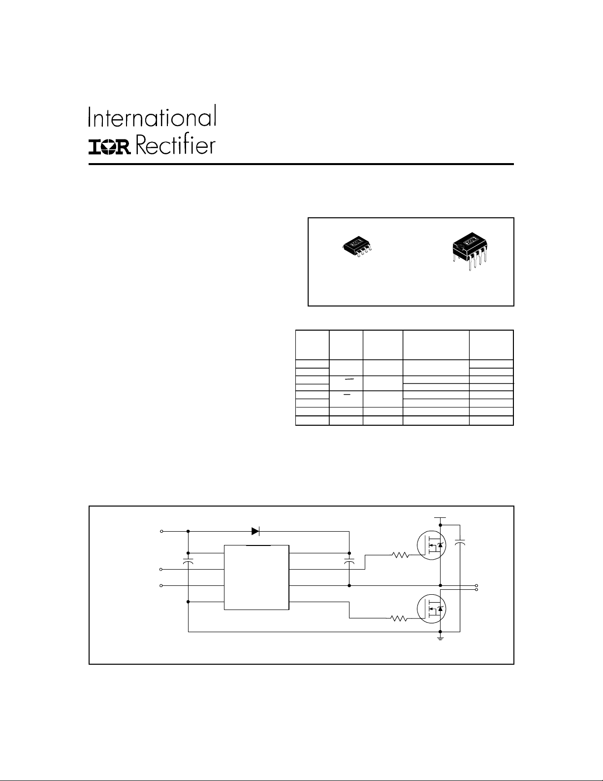
Packages
8-Lead SOIC - IR2308S
Also available
LEAD-FREE (PbF)
2106//2108//2109/2304/2308 Feature Comparison
Part
2106
21064
2108
21084
2109 Internal 540ns COM
21094
2304
2308
Input
logic
HIN/LIN no none
HIN/LIN yes
IN/SD yes
HIN/LIN
Crossconduction
prevention
logic
yes
yesHIN/LIN
Programmable 0.54~5µs
Programmable 0.54~5 µs
Internal 100ns
8-Lead PDIP
IR2308
Dead-Time Ground Pins
Internal 540ns COM
Internal 540ns COM
VSS/COM
VSS/COM
VSS/COM
COM
COM
Typical Connection
up to 600V
V
CC
V
CC
HIN
LIN
(Refer to Lead Assignments for correct pin configuration). This/These diagram(s) show electrical connections
only. Please refer to our Application Notes and DesignT ips for proper circuit board layout.
HIN
LIN
www.irf.com 1
V
HO
V
LOCOM
B
S
TO
LOAD
IR2308(S) & ( PbF)
Absolute Maximum Ratings
Absolute maximum ratings indicate sustained limits beyond which damage to the device may occur. All voltage parameters are absolute voltages referenced to COM. The thermal resistance and power dissipation ratings are measured
under board mounted and still air conditions.
Symbol Definition Min. Max. Units
V
B
V
S
V
HO
V
CC
V
LO
V
IN
dVS/dt Allowable offset supply voltage transient — 50 V/ns
P
D
Rth
JA
T
J
T
S
T
L
High side floating absolute voltage -0.3 625
High side floating supply offset voltage VB - 25 VB + 0.3
High side floating output voltage VS - 0.3 V
Low side and logic fixed supply voltage -0.3 25
Low side output voltage -0.3 VCC + 0.3
Logic input voltage (HIN & LIN ) VSS - 0.3 V
Package power dissipation @ TA ≤ +25°C (8 lead PDIP) — 1.0
(8 lead SOIC) — 0.625
Thermal resistance, junction to ambient (8 lead PDIP) — 125
(8 lead SOIC) — 200
Junction temperature — 150
Storage temperature -50 150
Lead temperature (soldering, 10 seconds) — 300
CC
B
+ 0.3
+ 0.3
V
W
°C/W
°C
Recommended Operating Conditions
The Input/Output logic timing diagram is shown in figure 1. For proper operation the device should be used within the
recommended conditions. The VS and VSS offset rating are tested with all supplies biased at 15V differential.
Symbol Definition Min. Max. Units
VB High side floating supply absolute voltage VS + 10 VS + 20
V
S
V
HO
V
CC
V
LO
V
IN
T
A
Note 1: Logic operational for VS of -5 to +600V. Logic state held for VS of -5V to -VBS. (Please refer to the Design Tip
DT97-3 for more details).
2 www.irf.com
High side floating supply offset voltage Note 1 600
High side floating output voltage V
Low side and logic fixed supply voltage 10 20
Low side output voltage 0 V
Logic input voltage COM V
Ambient temperature -40 125
S
V
CC
CC
B
°C
V
IR2308(S) & ( PbF)
Dynamic Electrical Characteristics
V
(VCC, VBS) = 15V, VSS = COM, CL = 1000 pF, TA = 25°C, DT = VSS unless otherwise specified.
BIAS
Symbol Definition Min. Typ. Max. Units Test Conditions
t
on
t
off
MT Delay matching | ton - t
t
t
DT Deadtime: LO turn-off to HO turn-on(DT
MDT Deadtime matching = | DT
Static Electrical Characteristics
V
BIAS
parameters are referenced to VSS/COM and are applicable to the respective input leads: HIN and LIN. The VO, IO and Ron
parameters are referenced to COM and are applicable to the respective output leads: HO and LO.
Symbol Definition Min. T yp. Max. Units T est Conditions
V
V
V
V
I
LK
I
QBS
I
QCC
I
IN+
I
IN-
V
CCUV+
V
BSUV+
V
CCUV-
V
BSUV-
V
CCUVH
V
BSUVH
I
O+
I
Turn-on propagation delay — 220 300 VS = 0V
Turn-off propagation delay — 200 280 VS = 0V or 600V
off
|
Turn-on rise time — 150 220 VS = 0V
r
Turn-off fall time — 50 80 VS = 0V
f
LO-HO) &
HO turn-off to LO turn-on (DT
LO-HO
(VCC, VBS) = 15V, VSS = COM, DT= VSS and TA = 25°C unless otherwise specified. The VIL, VIH and I
IH
IL
OH
OL
O-
Logic “1” input voltage for HIN & LIN 2.9 — — VCC = 10V to 20V
Logic “0” input voltage for HIN & LIN — — 0.8 VCC = 10V to 20V
High level output voltage, V
Low level output voltage, V
Offset supply leakage current — — 50 VB = VS = 600V
Quiescent VBS supply current 20 60 150 V
Quiescent VCC supply current 0.4 1.0 1.6 mA VIN = 0V or 5V
Logic “1” input bias current — 5 20 HIN = 5V, LIN = 5V
Logic “0” input bias current — 1 2 HIN = 0V, LIN = 0V
VCC and VBS supply undervoltage positive going 8.0 8.9 10
threshold
VCC and V
threshold
Hysteresis 0.3 0.7 —
Output high short circuit pulsed current 97 200 — VO = 0V,
Output low short circuit pulsed current 250 350 — VO = 15V,
supply undervoltage negative going 7.4 8.2 9.0
BS
BIAS
O
- V
- DT
O
HO-LO)
HO-LO
—046
400 540 680
—060
|
— 0.8 1.4 IO = 20 mA
— 0.3 0.6 IO = 20 mA
nsec
V
µA
µA
V
mA
IN
PW ≤ 10 µs
PW ≤ 10 µs
IN
= 0V or 5V
www.irf.com 3

IR2308(S) & ( PbF)
Functional Block Diagram
IR2308
HIN
VSS/COM
LEVEL
SHIFT
PULSE
GENERATOR
HV
LEVEL
SHIFTER
PULSE
FILTER
UV
DETECT
VB
R
Q
R
S
HO
VS
LIN
DT
VSS
DEADTIME &
SHOOT-THROUGH
PREVENTION
VSS/COM
LEVEL
SHIFT
DELAY
UV
DETECT
VCC
LO
COM
4 www.irf.com

Lead Definitions
Symbol Description
HIN Logic input for high side gate driver output (HO), in phase
LIN Logic input for low side gate driver output (LO), in phase
V
B
HO High side gate driver output
V
S
V
CC
LO Low side gate driver output
COM Low side return
High side floating supply
High side floating supply return
Low side and logic fixed supply
IR2308(S) & ( PbF)
Lead Assignments
1
V
CC
2
HIN
3
LIN
4
COM
8 Lead PDIP 8 Lead SOIC
V
HO
V
LO
8
B
7
6
S
5
1
V
CC
2
HIN
3
LIN
4
COM
Also available LEAD-FREE(PbF)
IR2308 IR2308S
www.irf.com 5
V
HO
V
LO
8
B
7
6
S
5

IR2308(S) & ( PbF)
LIN
HIN
50%
50%
LIN
HIN
HO
HO
LO
Figure 1. Input/Output Timing Diagram Figure 2. Switching Time Waveform Definitions
LIN
50
HIN
%
LO
50
%
90%
t
on
t
r
t
off
t
f
90% 90%
10% 10%
HO
LO
DT
MDT=
LO-HO
90%
DT
10%
LO-HO
- DT
DT
HO-LO
10%
HO-LO
Figure 3. Deadtime Waveform Definitions
IR WORLD HEADQUARTERS: 233 Kansas Street, El Segundo, California 90245 Tel: (310) 252-7105
Data and specifications subject to change without notice. 3/19/2003
6 www.irf.com
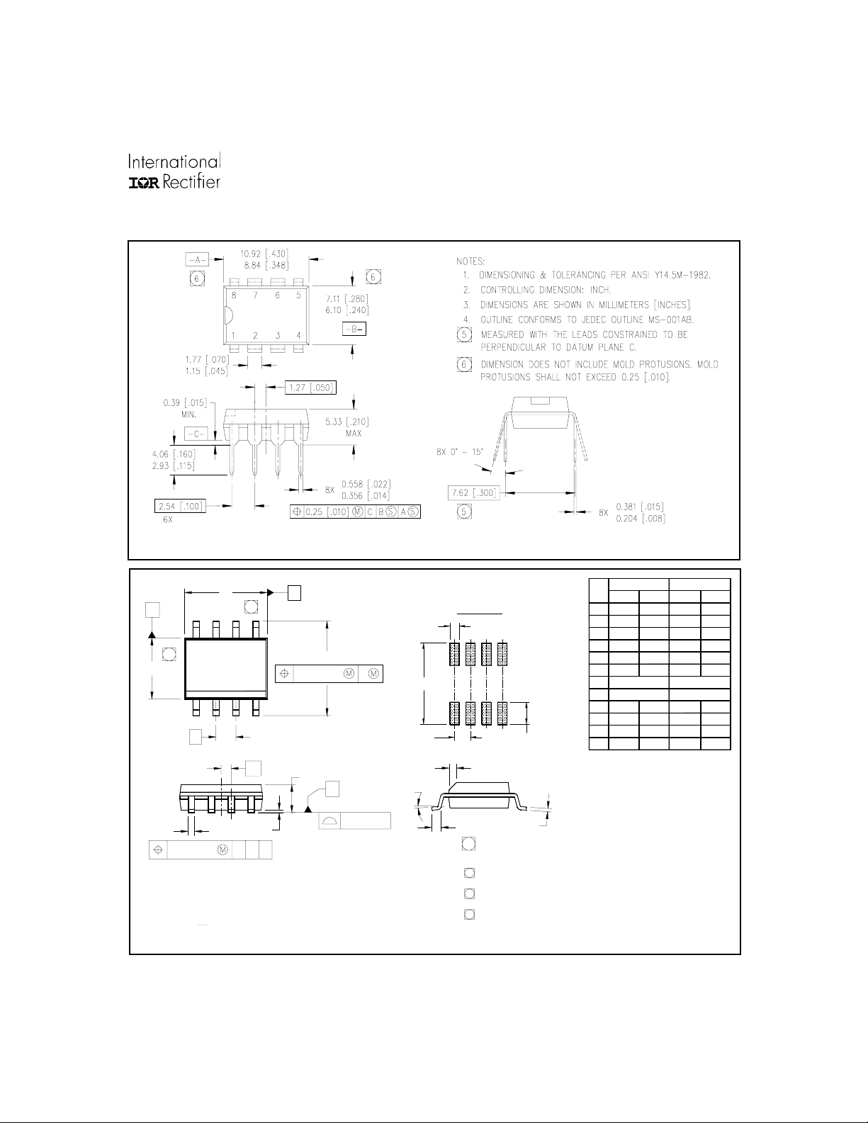
Case outlines
IR2308(S) & ( PbF)
A
E
D B
5
87
6
6X
65
H
4312
0.25 [ . 010 ] A
e
e1
A
C
8X b
0.25 [ . 010 ]
NOTES:
1. DIMENSIONING & TOLERANCING PER ASME Y14.5M-1994.
2. CONT ROLLING DIMENSION: MILLIMETER
3. D IMENSIONS ARE SHOW N IN MILL IMETERS [INCHES] .
4. OUTLINE CONFORMS TO JEDE C OUT L INE MS-01 2 A A .
A1
CAB
0.10 [ . 004 ]
8-Lead SOIC
8-Lead PDIP
6.46 [. 2 55]
3X 1.27 [. 05 0]
y
01-3003 01
DIM
FOOTPRINT
8X 0.72 [. 02 8]
8X 1.78 [. 07 0]
MIN MAX
.0532
A
A1
b
c .0075 .0098 0.19 0.25
D
E
e
e1
H
K
L
y
.0688
.0040
.0098
.020
.013
.1968
.189
.1574
.1497
.050 BASIC
.025 BASIC 0.635 BASIC
.2284
.2440
.0099
.0196
.016
.050
0°
K x 4 5°
8X L
8X c
7
5 DIMENSION DOES NOT INCLUDE MOLD PROTRUSIONS.
MOLD PROTRUSIONS NO T TO EXCEED 0.15 [.006].
6 DIMENSION DOES NOT INCLUDE MOLD PROTRUSIONS.
MOLD PROTRUSIONS NO T TO EXCEED 0.25 [.010].
7 DIMENSION IS THE LENGT H OF L EAD FOR SOLD ERING T O
A SUBSTRATE.
01-0021 11
8°
01-6014
(MS-001AB)
MILLIMETERSINC H E S
MIN MAX
1.35
1.75
0.10
0.25
0.33
0.51
4.80
5.00
3.80
4.00
1.27 BASIC
5.80
6.20
0.25
0.50
0.40
1.27
0°
8°
01-6027
(MS-012AA)
www.irf.com 7

IR2308(S) & ( PbF)
LEADFREE PART MARKING INFORMATION
Part number
Date code
Pin 1
Identifier
?
MARKING CODE
P
Lead Free Released
Non-Lead Free
Released
IRxxxxxx
YWW?
ORDER INFORMATION
Basic Part (Non-Lead Free)
8-Lead PDIP IR2308 order IR2308
8-Lead SOIC IR2308S order IR2308S
IR logo
?XXXX
Lot Code
(Prod mode - 4 digit SPN code)
Assembly site code
Per SCOP 200-002
Leadfree Part
8-Lead PDIP R2308 not available
8-Lead SOIC IR2308S order IR2308SPbF
Thisproduct has been designed and qualified for the industrial market.
Qualification Standards can be found on IR’s Web Site http://www.irf.com
IR WORLD HEADQUARTERS: 233 Kansas St., El Segundo, California 90245 Tel: (310) 252-7105
8 www.irf.com
Data and specifications subject to change without notice.
6/15/2004
 Loading...