IOR IR2159S, IR21591S User Manual
Preliminary Data Sheet No. PD60169-E
DIMMING BALLAST CONTROL IC
Features
Ballast control and half-bridge driver in one IC
•
T ransf ormer-less lamp power sensing
•
Closed-loop lamp power control
•
Closed-loop preheat current control
•
Programmable preheat time
•
Programmable preheat current
•
Programmable ignition-to-dim time
•
0.5 to 5VDC dimming control input
•
Min and max lamp power adjustments
•
Programmable minimum frequency
•
Internal current sense blanking
•
Full lamp fault protection
•
Description
Description: The IR2159/IR21591 are complete dimming ballast controllers and 600V
half-bridge drivers all in one IC. The architecture includes phase control for transformer-less lamp power sensing and regulation which minimizes changes needed to
adapt non-dimming ballasts for dimming. Externally programmable features such as
preheat time and current, ignition-to-dim time, and a complete dimming interface with
minimum and maximum settings provide a high degree of flexibility for the ballast
design engineer. Protection from failure of a lamp to strike , filament failures, thermal
overload, or lamp failure during normal operation, as well as an automatic restart
function, have been included in the design. The heart of this control IC is a voltagecontrolled oscillator with externally programmable minimum frequency. The IR2159/
IR21591 are available in both 16 pin DIP and 16 pin narrow body SOIC packages.
Brown-out protection
•
Automatic restart
•
Micro-power startup
•
Zener clamped V cc
•
Over-temperature protection
•
16-pin DIP and SOIC package types
•
Parameter IR2159 IR21591
Deadtime 1.8us 1.0us
Frequency
Range
IR2159
IR21591
See
Graph 3
Packages
16 Lead SOIC
(narrow body)
(S)
(S)
See
Graph 4
16 Lead PDIP
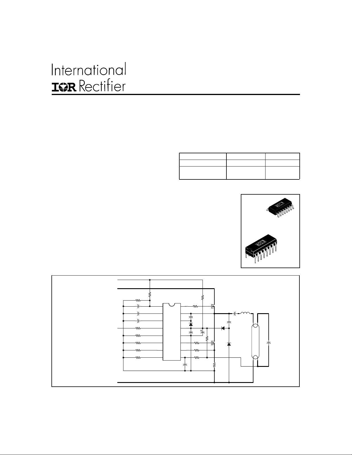
T ypical Connection
+ Rectified AC Line
+ DC Bus
0.5 to 5VDC
- DC Bus
R
VAC
R
VDC
C
VDC
1
C
VCO
C
PH
R
DIM
R
MAX
R
MIN
R
FMIN
R
IPH
VDC
2
VCO
3
CPH
DIM
5
MAX
6
MIN
7
FMIN
8 9
IPH
R
PULL-UP
16
HO
15
VS
14
VB
134
VCC
12
COM
11
LO
10
CS
SD
R
CS
www.irf.com 1
Single Lamp Dimmable
IR2159/IR21591
(S)
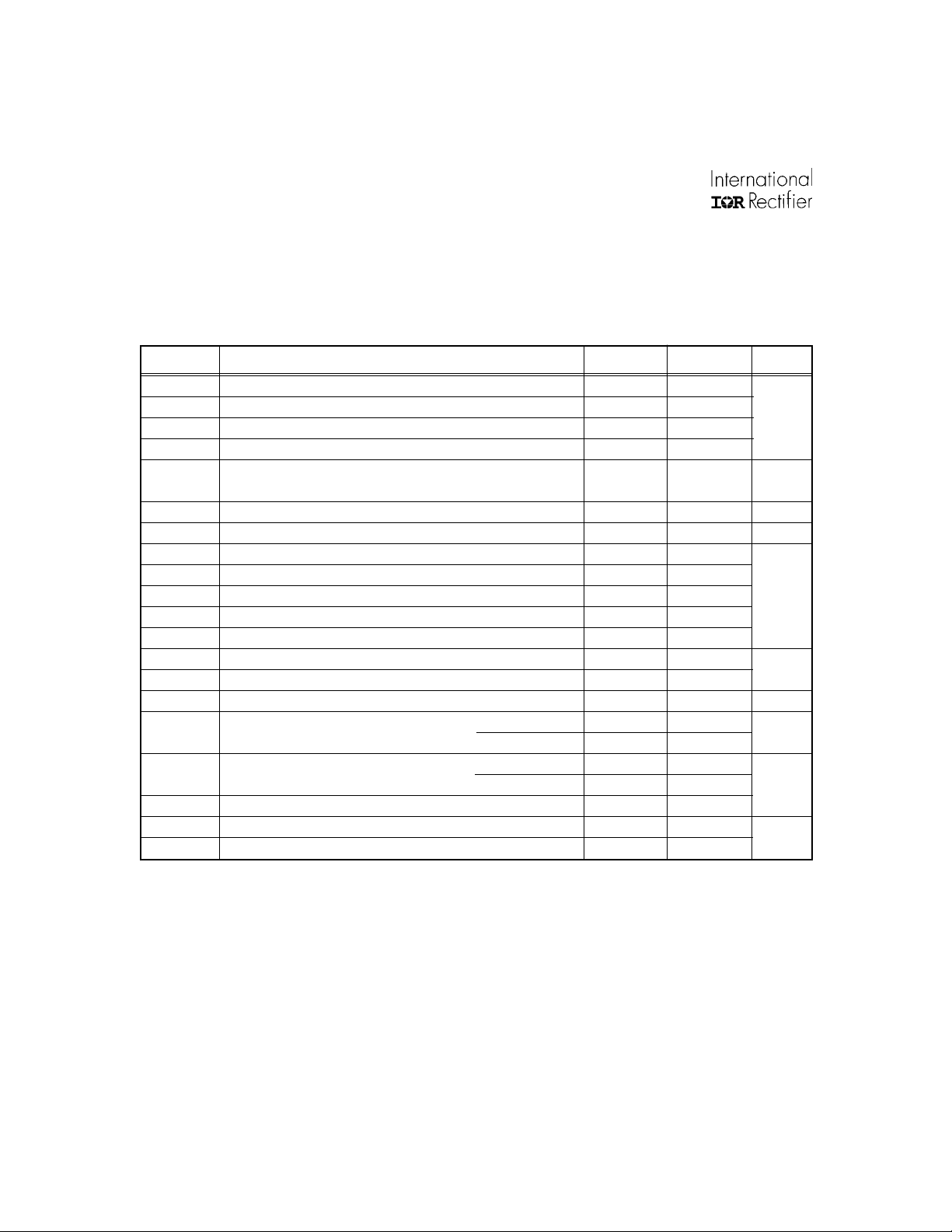
Absolute Maximum Ratings
Absolute maximum ratings indicate sustained limits beyond which damage to the device may occur. All voltage
parameters are absolute voltages referenced to COM, all currents are defined positive into any lead. The thermal
resistance and power dissipation ratings are measured under board mounted and still air conditions.
Symbol Definition Min. Max. Units
V
B
V
S
V
HO
V
LO
I
OMAX
V
VCO
I
CPH
V
IPH
V
DIM
V
MAX
V
MIN
V
CS
I
SD
I
CC
dV/dt Allowable offset voltage slew rate - 50 50 V/ns
P
D
Rth
JA
T
J
T
S
T
L
High side floating supply voltage -0.3 625
High side floating supply offset voltage VB - 25 VB + 25
High side floating output voltage VS - 0.3 V
B
+ 0.3
Low side output voltage -0.3 VCC + 0.3
Maximum allowable output current (either output) -500 500
due to external power transistor miller effect
mA
Voltage controlled oscillator input v oltage -0.3 6.0 V
CPH current -5 5 mA
IPH voltage -0.3 5.5
Dimming control pin input voltage -0.3 5.5
Maximum lamp power setting pin input voltage -0.3 5.5
V
Minimum lamp power setting pin input voltage -0.3 5.5
Current sense input voltage -0.3 5.5
Shutdown pin current -5 5
Supply current (note 1) — 25
Package power dissipation @ TA ≤ +25°C (16 pin DIP) — 1.60
P
D
(T
=
JMAX-TA
)/Rth
JA
(16 pin SOIC) — 1.25
Thermal resistance, junction to ambient (16 pin DIP) — 7 5
(16 pin SOIC) — 11 5
mA
W
o
C/W
Junction temperature -55 15 0
Storage temperature -55 15 0
o
Lead temperature (soldering, 10 seconds) — 300
V
C
Note 1: This IC contains a zener clamp structure between the chip VCC and COM which has a nominal breakdown
voltage of 15.6V (V
power source greater than the diode clamp voltage (V
). Please note that this supply pin should not be driven by a DC, low impedance
CLAMP
) as specified in the Electrical Characteristics
CLAMP
section.
2 www.irf.com
IR2159/IR21591
(S)
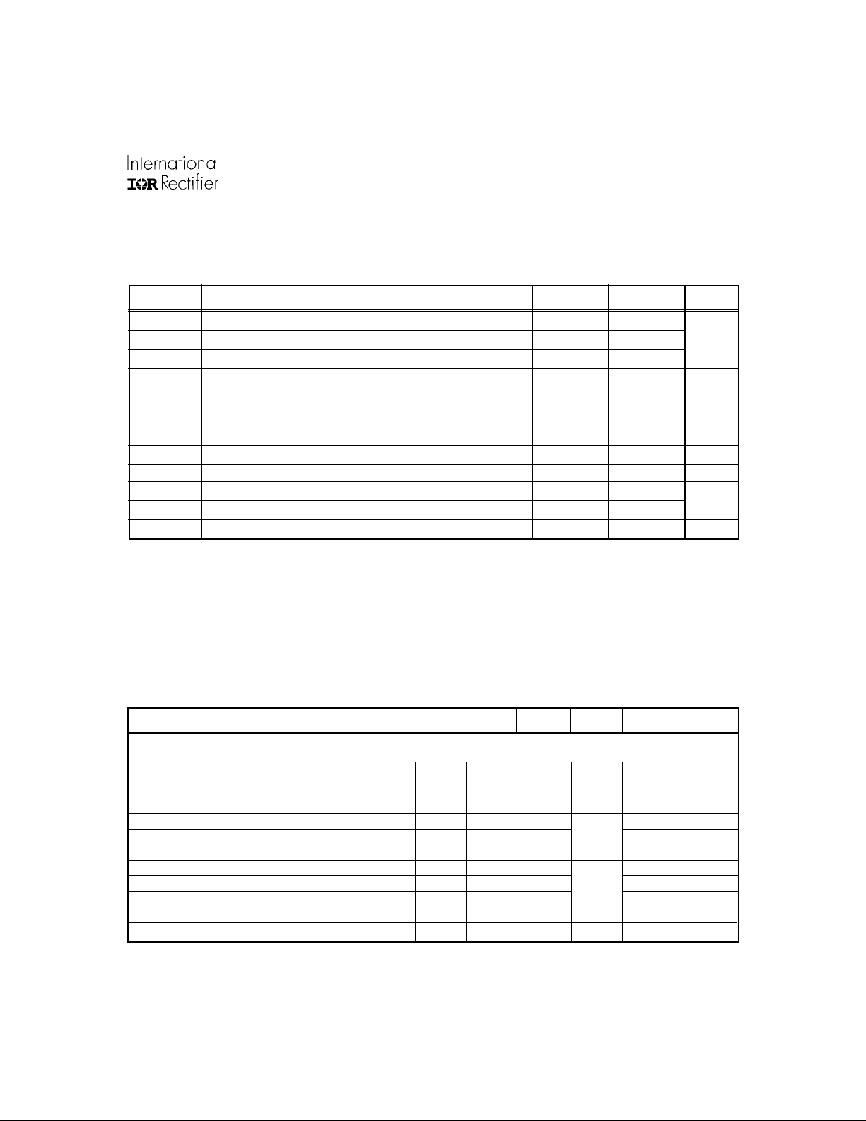
Recommended Operating Conditions
For proper operation the device should be used within the recommended conditions.
Symbol Definition Min. Max. Units
V
BS
V
S
V
CC
I
CC
V
VCO VCO pin voltage
V
DIM
V
MAX
V
MIN
R
FMIN
I
SD
I
CS
T
J
High side floating supply voltage VCC - 0.7 V
Steady state high side floating supply offset voltage -1 600
Supply voltage V
Supply current note 2 10 mA
DIM pin voltage 0 5
MAX pin current (note 3) -750 0
MIN pin voltage 1 3 V
Minimum frequency setting resistance 10 1 00
Shutdown pin current - 1 1
Current sensing pin current -1 1
Junction temperature -40 125
CCUV+VCLAMP (15.6)
05
CLAMP
V
V
µA
kΩ
mA
o
C
Note 2: Enough current should be supplied into the VCC lead to keep the internal 15.6V zener clamp diode on this lead
Note 3: The MAX lead is a voltage-controlled current source. For optimum dim interface current mirror performance,
regulating its voltage, V
this current should be kept between 0 and 750µA.
CLAMP
.
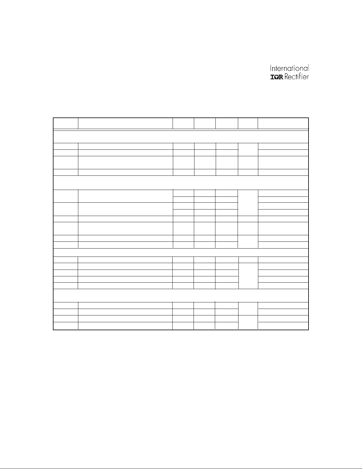
Electrical Characteristics
VCC = VBS = V
R
= 56k, V
MIN
Symbol Definition Min. Typ. Max. Units Test Conditions
Supply Characteristics
V
CCUV+ VCC
V
CCHYS VCC
I
QCCUV
I
QCCFLT
I
QCCFMIN VCC
I
QCCFMAX VCC
I
QCCFMIN VCC
I
QCCFMAX VCC
V
CLAMP VCC
= 14V +/- 0.25V, VCS = 0.5V, VSD = 0.0V, R
BIAS
= 0.0V, C
CPH
supply undervoltage positive going 12.0 12.5 13.0
threshold
supply undervoltage lockout hysteresis 1.5 1.6 1.7
UVLO mode quiescent current — 200 — VCC = 10V
Fault-mode quiescent current — 240 — SD=5V, CS=2V, or
supply current @ FMIN (IR2159) — 5.6 — V
supply current @ FMAX (IR2159) — 6.6 — V
supply current @ FMIN (IR21591) — 5.4 — V
supply current @ FMAX (IR21591) — 6.8 — V
zener shunt clamp voltage 14.5 15.6 16.5 V ICC = 10mA
= 1000pF, TA = 25oC unless otherwise specified.
LO,HO
FMIN
= 40k, C
VCO
= 10 nF, V
= 0.0V, R
DIM
V
µA
mA
MAX
Tj > TSD
VCO
VCO
VCO
VCO
= 33k,
= 0V
= 5V
= 0V
= 5V
www.irf.com 3
IR2159/IR21591
(S)
Electrical Characteristics (cont.)
VCC = VBS = V
R
= 56k, V
MIN
Symbol Definition Min. Typ. Max. Units Test Conditions
Floating Supply Characteristics
I
QBS0
I
QBS1
V
BSMIN
I
LK
Oscillator I/O Characteristics
f
vco
f
vco
d Gate drive outputs duty cycle
V
VCOFLT
IVCOPH Preheat mode VCO pin discharge current
IVCODIM Dim mode VCO pin discharge current
= 14V +/- 0.25V, VCS = 0.5V, VSD = 0.0V, R
BIAS
= 0.0V, C
TPH
Quiescent VBS supply current — 0 — VHO = V
Quiescent VBS supply current —
Minimum required VBS v oltage for proper
HO functionality
Offset supply leakage current — — 50
VCO frequency range (IR2159) — 25 —
(See graph 3) —
VCO frequency range (IR21591) — 30 —
(See graph 4) —
Fault-mode VCO pin voltage (UVLO,
shutdown, over-current/temp.)
= 1000pF, TA = 25oC unless otherwise specified.
LO,HO
= 40k, C
FMIN
— 4
—
—
—
1.0
—
VCO
30
95
230
50
5 V
16.0
= 10 nF, V
—V
5 V
—
—
—
—
—
= 0.0V, R
DIM
µA
µA
kHz
% V
µA
MAX
= V
HO
VB = VS = 600V
V
=0V, RFMIN=39KΩ
VCO
V
=5V, RFMIN=10KΩ
VCO
V
=0V, RFMIN=68KΩ
VCO
V
=5V, RFMIN=10KΩ
VCO
VCO
VCPH < 5V
= 33k,
S
B
= 0V
IVCOPK
t
DTLO
t
DTHO
t
DTLO
t
DTHO
Amplitude control VCO pin charging current — 60.0 —
LO output deadtime (IR2159)
HO output deadtime (IR2159)
LO output deadtime (IR21591)
HO output deadtime (IR21591)
— 1.8 —
— 1.8 —
— 1.0 —
— 1.0 —
µA
µs
V
CPH
< 5V, V
CS
Gate Driver Output Characteristics
VOL Low-level output voltage — — 100
VOH High-level output voltage — — 100 V
tr Turn-on rise time — — 150
tf T urn-off fall time
—
—
100
4 www.irf.com
mV
ns
BIAS
- Vo
>
V
IPH
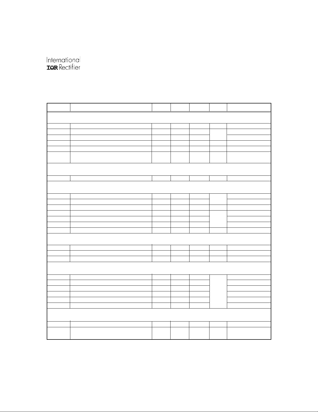
IR2159/IR21591
(S)
Electrical Characteristics (cont.)
VCC = VBS = V
R
= 56k, V
MIN
Symbol Definition Min. Typ. Max. Units Test Conditions
Preheat Characteristics
ICPH CPH pin charging current
VCPHIGN CPH pin ignition mode threshold voltage
VCPHCLMP CPH pin clamp voltage —
IIPH IPH pin DC source current — 25.0 — µAIIPH = 1/RFMIN
VCSTH Peak preheat current regulation threshold — 0.7 — V VCSTH =(IIPH) x (RIPH)
VCPHFLT CPH pin voltage during UVLO or fault —
Ignition Characteristics
V
CSTH
Protection Characteristics
V
SDTH+
V
VDCTH+
V
SDHYS
V
VDCHYS
V
SDCLMP
V
CSTH
T
SD
= 14V +/- 0.25V, VCS = 0.5V, VSD = 0.0V, R
BIAS
= 0.0V, C
TPH
Peak over current threshold — 1.6 — V VCPH < 5V
Rising shutdown pin threshold voltage — 2.0 —
Rising VDC pin threshold voltage — 5. 1 —
SD threshold hysteresis — 150 — mV
VDC threshold hysteresis — 2. 1 —
SD pin clamp voltage — 7. 6 — ISD = 100mA
Peak ov er-current latch threshold voltage — 1.6 —
Thermal shutdown junction temperature —
= 1000pF, TA = 25oC unless otherwise specified.
LO,HO
—
—
FMIN
= 40k, C
1.3
5.0
10
0.0
165 —
VCO
= 10 nF, V
—
—
—
—
= 0.0V, R
DIM
µA
V
V SD = 5V, or CS = 2V,
or Tj
V
V
o
C
V
MAX
CPH
= 33k,
> TSD
>
5.1V
Phase Control
V
CSTHZX
R
FB
t
Blank
Zero-crossing threshold voltage — 0.0 — V
Phase control FB resistor (Internal) — 5.7 — kΩ
Zero-crossing internal blank time — 400 — ns
Dimming Interface
V
DIMOFF
V
DIM
V
MINMIN
V
MINMAX
V
DIMTH
V
DIMTH DIM mode VCO Threshold (IR21591)
Minimum Frequency Setting
V
FMIN
V
FMINFLT
www.irf.com 5
DIM pin offset voltage — 0.5 —
DIM pin input voltage range 0.0 — 5.0
DIM minimum reference voltage (MIN pin) — 1.0 —
DIM maximum reference voltage (MIN pin) — 3.0 —
DIM mode VCO Threshold (IR2159) — 0.5 —
— 1.1 —
FMIN pin voltage during normal operation — 5.1 — V
FMIN pin voltage during fault mode — 0.0 — V
V
= 5V
DIM
V
V
= 0V
DIM
SD = 5V, or CS = 2V,
or Tj
> TSD
IR2159/IR21591
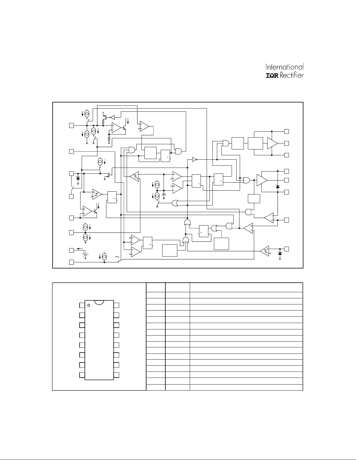
Block Diagram
(S)
5.1V
VCC
I
R
FB
15uA
1.3uA
RQ
I
DIM
4/R
FMIN
I
/5
DIM
1/R
1.6V
FMIN
CT
V
DIMTH
10 CYCLES
IGNITION
COUNTER
IDT+I
RQ
CT
I
CT
CT
QS
REF
QS
FB
3V
5.1V
1
0
VCO
VDC
CPH
DIM
MAX
MIN
FMIN
IPH
60uA
2
1uA
1
3
10V
4
5
6
I
FMIN
7
5.1V
8
Lead Assignments & Definitions
QS
RQ
5.1V
1.0V
CT
UNDER-
VOLTAGE
DETECT
14
VB
SHIFT
PULSE
FILTER &
LATCH
400ns
DELAY
15.6V
2.0V
7.6V
16
HO
15
VS
13
VCC
11
LO
12
COM
10
CS
9
SD
LEVEL
ERR
T
R1
R2 Q
QS
QS
Q
RQ
RQ
OVER-
TEMP
DETECT
Pin Assignments
1
VDC
2
VCO
3
CPH
4
DIM
5
MAX
6
MIN
7
FMIN
8
IPH
16
HO
15
VS
14
VB
13
VCC
12
COM
11
LO
10
CS
9
SD
Pin # Symbol Description
Line input voltage detection
Voltage controlled oscillator Input
Preheat timing input
0.5 to 5VDC dimming control input
Maximum lamp power setting
Minimum lamp power setting
Minimum frequency setting
Shutdown input
Current sensing input
Low-side gate driver output
IC power & signal ground
Logic & low-side gate driver supply
High-side gate driver floating supply
High voltage floating return
High-side gate driver output
15
10
11
12
13
14
16
1
2
3
4
5
6
7
8
9
VDC
VCO
CPH
DIM
MAX
MIN
FMIN
IPH Peak preheat current reference
SD
CS
LO
COM
VCC
VB
VS
HO
6 www.irf.com
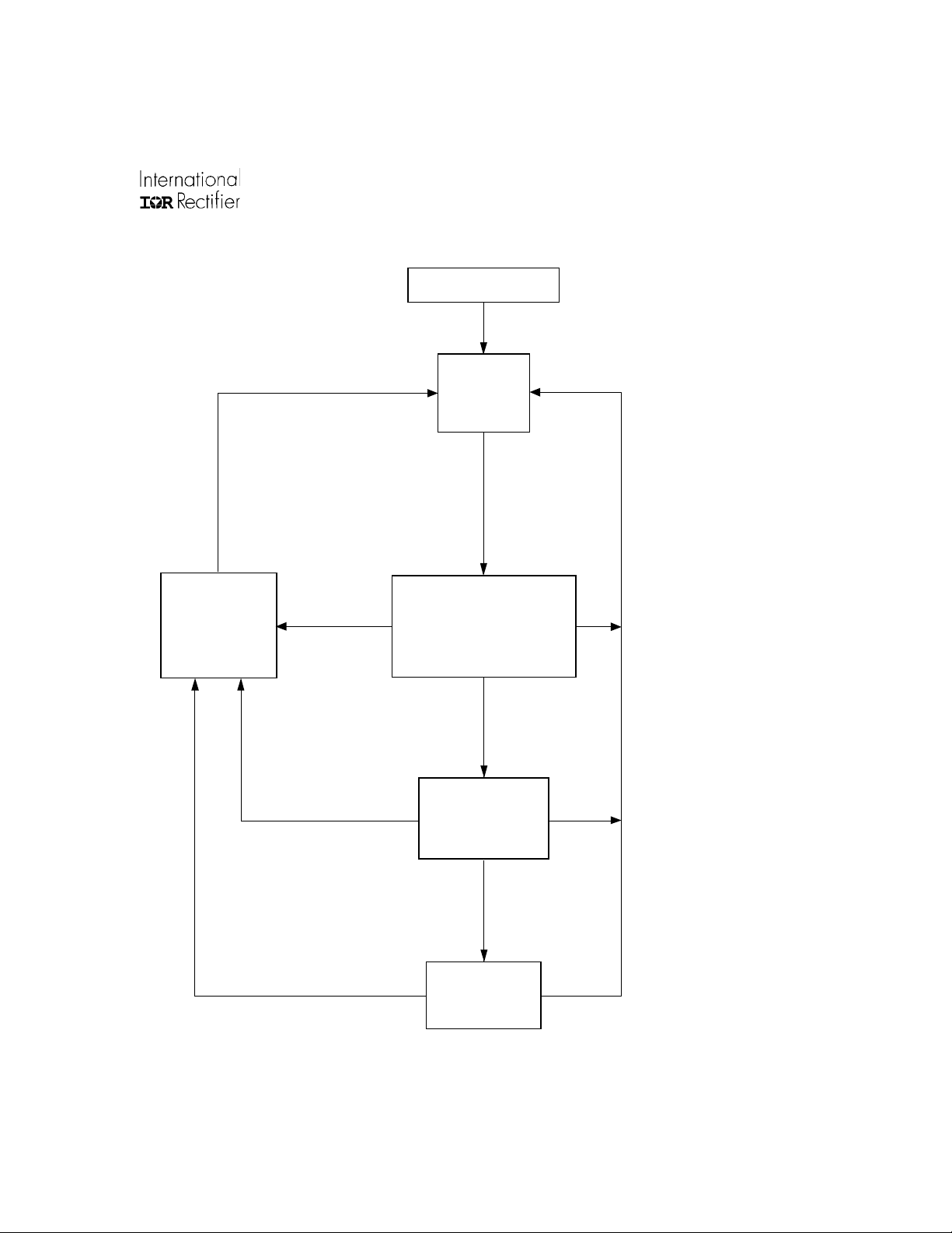
State Diagram
(
g)
(
)
Power Turned On
UVLO Mode
1/2-Bridge Off
IQCC=200mA
CPH=0V
Oscillator Off
IR2159/IR21591
(S)
SD > 2.0V
(Lamp Removal)
or
VCC < 10.9V
(Power Turned Off)
FAULT Mode
Fault Latch Set
1/2-Bridge Off
I
=240µA
QCC
CPH=0V
VCC=15.6V
Oscillator Off
CS > V
CSTH
(Over-Current or Hard Switching)
or
TJ > 165C
(Over-Temperature)
TJ > 165C
(Over-Temperature)
CS > V
CSTH
Failure to Strike Lamp
or Hard Switchin
or
TJ> 165C
Over-Temperature
(1.6V)
(1.6V)
PREHEAT Mode
1/2-BridgeOscillator On
V
(Peak Current Control)
CSPK+VIPH
CPH Charging@I
DIM+Open Circuit
Over-Current Disabled
IGNITION Mode
fPH ramps to fMIN
CPH Charging@I
DIM=Open Circuit
Over-Current Enabled
DIM Mode
PhaseCS=Phase
DIM=CPH
Over-Current Enabled
and
and
and
+1µA
+1µA
REF
DIMTH
(UV+)
(Bus OK)
(Lamp OK)
(T
jmax
VCC > 12.5V
VDC > 5.1V
SD < 1.7V
TJ < 165C
PH
CPH > 5.1V
(End of PREHEAT Mode)
PH
VCO < V
(End of IGNITION Mode)
VCC < 10.9V
(VCC Fault or Power Down)
or
VDC < 3.0V
(dc Bus/ac Line Fault or Power Down)
or
SD > 2.0V
)
(Lamp Fault or Lamp Removal)
www.irf.com 7
IR2159/IR21591
(S)
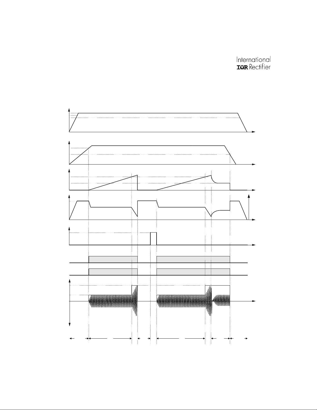
Timing Diagram
Non-strike fault condition with lamp exchange
VCC
15.6V
UVLO+
UVLO-
VDC
VDCTH+
VDCTH-
CPH
5.1V
V
DIM
VCO
SD
HO
LO
CS
1.6V
V
5V
5V
IPH
PH FLT
IGN
SD PH
IGN
DIM UVLOUVLO
f
8 www.irf.com
 Loading...