Data Sheet No. PD60206 Rev.C
IR2085S & (PbF)
HIGH SPEED, 100V, SELF OSCILLATING 50% DUTY CYCLE,
HALF-BRIDGE DRIVER
Features
Simple primary side control solution to enable half-bridge
•
DC-Bus Converters for 48V distributed systems with reduced
component count and board space.
Integrated 50% duty cycle oscillator & half-bridge driver IC in a
•
single SO-8 package
Programmable switching frequency with up to 500kHz max per
•
channel
+/- 1A drive current capability optimized for low charge MOSFETs
•
Adjustable dead-time 50nsec – 200nsec
•
Floating channel designed for bootstrap operation up to +100Vdc
•
High and low side pulse width matching to +/- 25nsec
•
Adjustable overcurrent protection
•
Undervoltage lockout and internal soft start
•
Also available LEAD-FREE
•
Description
The IR2085S is a self oscillating half-bridge driver IC with 50% duty cycle ideally
suited for 36V-75V half-bridge DC-bus converters. This product is also suitable for
push-pull converters without restriction on input voltage.
Product Summary
V
V
High/low side
output freq (f
Output Current (I
High/low side pulse
width matching +/- 25ns
25V
CC (max)
offset(max)
100Vdc
) 500kHz
osc
)
O
+/-1.0A(typ.)
Package
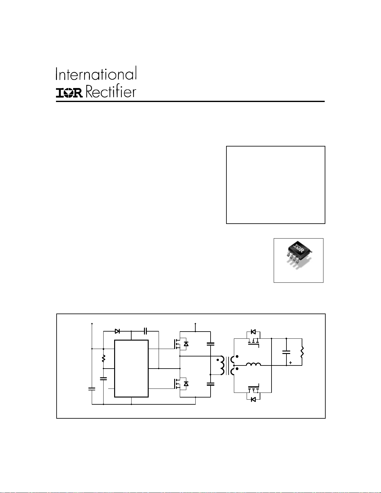
Each channel frequency is equal to f
where f
and can range from 50 to 200nsec. Internal soft-start increases the pulse width during
power up and maintains pulse width matching for the high and low outputs throughout the start up cycle. The
IR2085S initiates a soft start at power up and after every overcurrent condition. Undervoltage lockout prevents
operation if VCC is less than 7.5Vdc.
≈ 1/(2*R
osc
Vbias
C
BIAS
T.CT
(10-15V)
R
T
C
T
). Dead-time can be controlled through proper selection of C
D
BOOT
V
b
V
cc
OSC
IR2085
Cs
GND
C
HO
LO
V
BOOT
s
, where f
osc
can be set by selecting RT & CT,
osc
( 100V max)
Vin
S
1
S
2
C
2
C
1
SO -8SO -8
T
S
R1
L
S
R2
R
C
V
o
Simplified Circuit Diagram
www.irf.com
1

IR2085S & (PbF)
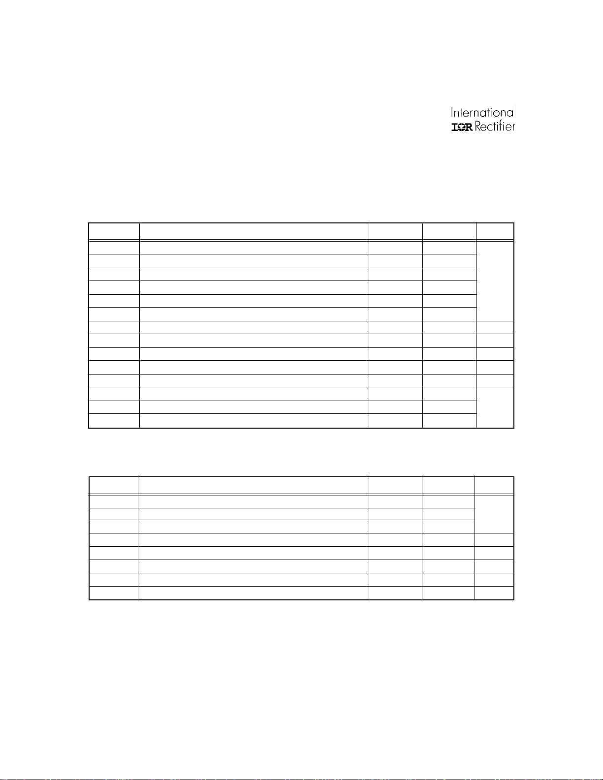
Absolute Maximum Ratings
Absolute maximum ratings indicate sustained limits beyond which damage to the device may occur. All voltage parameters are absolute voltages referenced to COM. All currents are defined positive into any lead. The thermal resistance
and power dissipation ratings are measured under board mounted and still air conditions.
Symbol Definition Min. Max. Units
V
b
V
CC
V
S
V
HO
V
LO
OSC OSC pin voltage -0.3 VCC + 0.3
V
CS
dVS/dt Allowable offset voltage slew rate -50 +50 V/ns
I
CC
P
D
Rth
JA
T
J
T
S
T
L
High side floating supply voltage -0.3 150
Low side supply voltage — 25
High side floating supply offset voltage Vb - 25 Vb + 0.3
High side floating output voltage Vb - 0.3 V
Low side output voltage -0.3 VCC + 0.3
Cs pin voltage -0.3 VCC + 0.3
Supply current — 20 mA
Package power dissipation
Thermal resistance, junction to ambient — 200 °C/W
Junction temperature -55 150
Storage temperature -55 150
Lead temperature (soldering, 10 seconds) — 300
— 1.0 W
b
+ 0.3
°C
V
Recommended Operating Conditions
For proper operation the device should be used within the recommended conditions.
Symbol Definition Min. Max. Units
Vb High side floating supply voltage Vdd -0.7 15
V
S
V
CC
I
CC
R
T
C
T
fosc(max) Operating frequency (per channel) — 500
T
J
Note1: Care should be taken to avoid output switching conditions where the Vs node flies inductively below ground by more
than 5V.
2
Steady state high side floating supply offset voltage -5 100
Supply voltage 10 15
Supply current (Note 2) — 5 mA
Timing resistor 10 100 KΩ
Timing capacitor 47 1000 pF
Junction temperature -40 125 °C
Vdc
KHz
www.irf.com

IR2085S & (PbF)
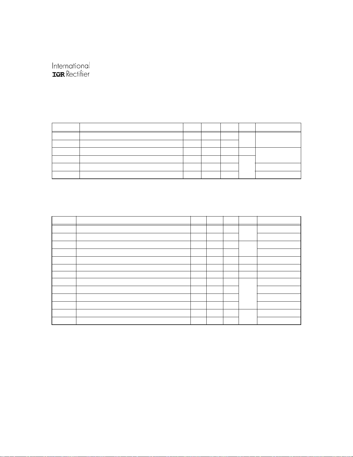
Dynamic Electrical Characteristics
V
(VCC, VBS) = 12V, C
BIAS
Symbol Definition Min. Typ. Max. Units Test Conditions
t
t
fosc Per channel output frequency 500 — — KHz
tdt High/low output dead time 50 — —
t
dcs
PM High/low pulse width mismatch -25 — 25 VS = 0V ~ 100V
Turn-on rise time — 40 60
r
Turn-off fall time — 20 30
f
Overcurrent shut down delay — 200 — pulse on CS
Static Electrical Characteristics
V
(VCC, VBS) = 12V, C
BIAS
Symbol Definition Min. Typ. Max. Units Test Conditions
V
OH
V
OL
I
leak
I
QBS
I
QCC
V
CS+ Overcurrent shutdown threshold
V
CS- Overcurrent shutdown threshold
U
VCC+
U
VCC-
U
VBS+
U
VBS-
I
O+
I
O-
High level output voltage, (V
Low level output voltage — — 0.1
Offset supply leakage current — — 50
Quiescent VBS supply current — — 150
Quiescent VCC supply current — — 1.5 mA
Undervoltage positive going threshold 6.8 7.3 7.8
Undervoltage negative going threshold 6.3 6.8 7.3
High side undervoltage positive going threshold 6.8 7.3 7.8
High side undervoltage negative going threshold 6.3 6.8 7.3
Output high short circuit current — 1.0 —
Output low short circuit current — 1.0 —
= 1000 pF, and TA = 25°C unless otherwise specified.
LOAD
= 1000 pF and TA = 25°C unless otherwise specified.
LOAD
- VO) — — 1.5
BIAS
250 300 350 mV
150 200 250 mV
nsec
nsec
V
µA
V
A
VS = 0V
CT =100pF,
RT =10Kohm
www.irf.com
3
 Loading...