

查询HFA04SD60S供应商
Ultrafast, Soft Recovery Diode
Bulletin PD-20617 rev. B 07/02
HFA04SD60S
Features
• Ultrafast Recovery Time
• Ultrasoft Recovery
• Very Low I
• Very Low Q
• Guaranteed Avalanche
• Specified at Operating Temperature
RRM
rr
Benefits
• Reduced RFI and EMI
• Reduced Power Loss in Diode and
Switching Transistor
• Higher Frequency Operation
• Reduced Snubbing
• Reduced Parts Count
Description/ Applications
These diodes are optimized to reduce losses and EMI/RFI in
high frequency power conditioning systems. The softness of
the recovery eliminates the need for a snubber in most
applications. These devices are ideally suited for freewheeling,
flyback, power converters, motor drives, and other applications
where high speed and reduced switching losses are design
requirements.
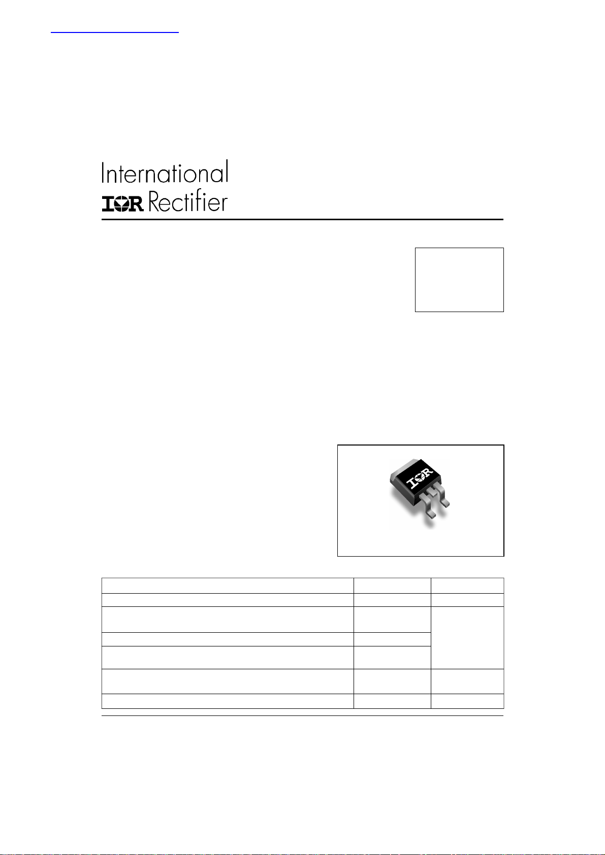
Package Outline
I
F(AV)
D - PAK
t
= 38ns
rr
= 4Amp
VR = 600V
Absolute Maximum Ratings
Parameters Max Units
V
RRM
I
F(AV)
I
FSM
I
FRM
P
D
TJ, T
Cathode-to-Anode Voltage 600 V
Continuous Forward Current 4 A
TC = 100°C
Single Pulse Forward Current 25
Peak Repetitive Forward Current 16
TC = 116°C
Maximum Power Dissipation 10 W
TC = 100°C
Operating Junction and Storage Temperatures - 55 to 150 °C
STG
www.irf.com
1
HFA04SD60S
Bulletin PD-20617 rev. B 07/02
Electrical Characteristics @ T
Parameters
VBR, VrBreakdown Voltage, 600 - - V IR = 100µA
Blocking Voltage
V
F
I
R
C
T
L
S
Forward Voltage - 1.5 1.8 V IF = 4A
See Fig. 1 - 1.8 2.2 V IF = 8A
Max. Reverse Leakage Current - 0.17 3.0 µA VR = VR Rated
Junction Capacitance - 4 8 pF VR = 200V
Series Inductance - 8.0 - nH Measured lead to lead 5mm from package body
= 25°C (unless otherwise specified)
J
Min Typ
- 1.4 1.7 V IF = 4A, TJ = 125°C
- 44 300 µA TJ = 125°C, VR = 0.8 x VR Rated
Max Units
Test Conditions
Dynamic Recovery Characteristics @ TJ = 25°C (unless otherwise specified)
Parameters
di
t
I
Q
rr
RRM
rr
(rec)
Reverse Recovery Time - 17 - ns IF = 1.0A, diF/dt = 200A/µA, VR = 30V
Peak Recovery Current - 2.9 5.2 A TJ = 25°C
Reverse Recovery Charge - 40 60 nC TJ = 25°C
/dt Rate of Fall of recovery Current - 280 - TJ = 25°C
M
Min
Typ Max Units Test Conditions
-2842 TJ = 25°C
-3857 TJ = 125°C
- 3.7 6.7 TJ = 125°C
- 70 105 TJ = 125°C
A/µs
- 235 - TJ = 125°C
I
= 4A
F
VR = 200V
diF /dt = 200A/µs
Thermal - Mechanical Characteristics
Parameters Min Typ Max Units
T
J
T
Stg
T
S
R
thJC
R
thJA
Wt Weight - 2.0 - g
T Mounting Torque 6.0 - 12 Kg*cm
! Typical Socket Mount
2
Max. Junction Temperature Range - - - 55 to 150 °C
Max. Storage Temperature Range - - - 55 to 150
Soldering Temperature, 10 sec - - 240
Thermal Resistance, Junction to Case - - 5.0 °C/ W
!
Thermal Resistance, Junction to Ambient - - 80
- 0.07 - (oz)
5.0 - 10 lbf*in
www.irf.com
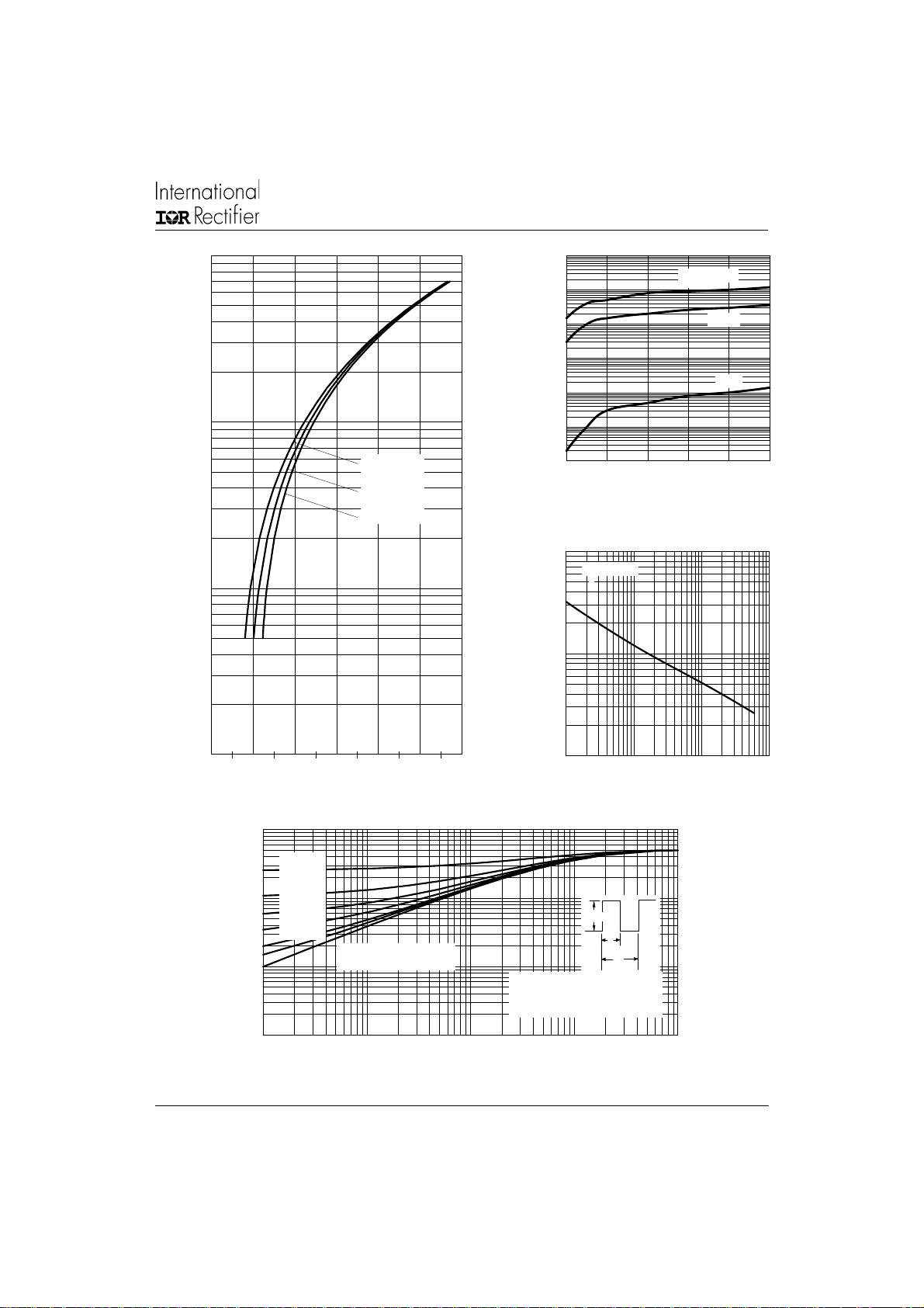
0.1
1
10
00
0123456
T = 150˚C
T = 125˚C
T = 25˚C
J
J
J
1000
100
HFA04SD60S
Bulletin PD-20617 rev. B 07/02
T = 150˚C
J
(A)
F
Instantaneous Forward Current - I
Forward Voltage Drop - VFM (V)
Fig. 1 - Typical Forward Voltage Drop Characteristics
10
(µA)
R
10
125˚C
1
0.1
0.01
Reverse Current - I
0.001
0 100 200 300 400 500
Reverse Voltage - VR (V)
Fig. 2 - Typical Values Of Reverse Current
Vs. Reverse Voltage
100
T = 25˚C
J
(pF)
T
10
Junction Capacitance - C
1
1 10 100 1000
Reverse Voltage - VR (V)
Fig. 3 - Typical Junction Capacitance
Vs. Reverse Voltage
25˚C
(°C/W)
thJC
1
www.irf.com
0.1
Thermal Impedance Z
.01
0.00001 0.0001 0.001 0.01 0.1
D = 0.50
D = 0.20
D = 0.10
D = 0.05
D = 0.02
D = 0.01
Single Pulse
(Thermal Resistance)
t1, Rectangular Pulse Duration (Seconds)
Fig. 4 - Max. Thermal Impedance Z
P
DM
t
1
t
2
Notes:
1. Duty factor D = t1/ t2
2. Peak Tj = Pdm x ZthJC + Tc
Characteristics
thJC
3

HFA04SD60S
100
1000
100 1000
If = 8A
If = 4A
Vr = 200V
Tj = 125˚C
Tj = 25˚C
Bulletin PD-20617 rev. B 07/02
50
If = 8A
If = 4A
40
14
12
10
If = 8A
If = 4A
8
trr (ns)
Irr (A)
6
30
4
Vr = 200V
Tj = 125˚C
Tj = 25˚C
20
100 1000
di
/dt (A/ µs)
F
2
0
100 1000
Average Forward Current - I
Vr = 200V
Tj = 125˚C
Tj = 25˚C
Fig. 5 - Typical Reverse Recovery vs. di F /dt Fig. 6 - Typical Recovery Current vs. di
200
Vr = 200V
Tj = 125˚C
180
Tj = 25˚C
160
F(AV)
(A)
/dt
F
4
140
120
100
Qrr ( nC )
If = 8A
If = 4A
80
60
40
20
100 1000
di
/dt (A/µs )
F
Fig. 7 - Typical Stored Charge vs. di
/ dt (A/ µs)
(rec)M
di
di F /dt (A/µs )
/dt
F
Fig. 8 - Typical di
(rec)M
/dt vs. di
/dt
F
www.irf.com

Reverse Recovery Circuit
V = 200V
R
0.01
Ω
L = 70µH
D.U.T.
HFA04SD60S
Bulletin PD-20617 rev. B 07/02
di F /dt
dif/dt
ADJUST
G
Fig. 9- Reverse Recovery Parameter Test Circuit
I
F
t
a
0
1
di F /dt
di /dt
f
1. diF/dt - Rate of change of current through zero
crossing
2. I
- Peak reverse recovery current
RRM
3. t
- Reverse recovery time measured from zero
rr
crossing point of negative going IF to point where
a line passing through 0.75 I
extrapolated to zero current
RRM
and 0.50 I
RRM
3
2
D
IRFP250
S
t
rr
t
b
Q
I
RRM
0.5
di(rec)M/dt
0.75
I
RRM
4. Qrr - Area under curve defined by t
and I
RRM
Q
rr
5. di
/dt - Peak rate of change of
(rec)M
current during tb portion of t
I
=
rr
RRM
t rr x I
4
5
rr
RRM
2
rr
www.irf.com
Fig. 10 - Reverse Recovery Waveform and Definitions
5

HFA04SD60S
C
Bulletin PD-20617 rev. B 07/02
Outline Table
6.73 (0.26)
6.35 (0.25)
5.46 (0.21)
5.21 (0.20)
4
1.64 (0.02)
123
1.52 (0.06)
1.15 (0.04)
1.14 (0.04)
2x
0.76 (0.03)
2.28 (0.09)
2x
4.57 (0.18)
1.27 (0.05)
0.88 (0.03)
6.22 (0.24)
5.97 (0.23)
0.89 (0.03)
3x
0.64 (0.02)
2.38 (0.09)
2.19 (0.08)
10.42 (0.41)
9.40 (0.37)
1 - Anode
1 - Cathode
2 - Cathode
2 - Cathode
3 - Anode
3 - Anode
4 - Cathode
4 - Cathode
1.14 (0.04)
0.89 (0.03)
0.58 (0.02)
0.46 (0.02)
6.45 (0.24)
5.68 (0.22)
0.51 (0.02)
MIN.
0.58 (0.02)
0.46 (0.02)
MINIMUM RECOMMENDED FOOTPRINT
5.97 (0.24)
6.48 (0.26)
2x
2.54 (0.10)
1.65 (0.06)
2x
2.28 (0.09)
Base
Common
Cathode
10.67 (0.42)
2x
4
Conform to JEDEC outline D-Pak
Dimensions in millimeters and (inches)
Tape & Reel Information
TRR
FEED DIRECTION
TRL
FEED DIRECTION
360 (14.173)
DIA. M AX.
13.5 0 (0.5 32)
12.8 0 (0.5 04)
1.85 (0.073)
1.65 (0.065)
DIA.
4.10 (0.161)
3.90 (0.153)
10.9 0 (0.4 29)
10.7 0 (0.4 21)
1.60 (0.063)
1.50 (0.059)
1.60 (0. 063)
1.50 (0. 059)
11.6 0 (0.4 57)
11.4 0 (0.4 49)
1.75 (0.069)
1.25 (0.049)
16.1 0 (0.6 34)
15.9 0 (0.6 26)
26.4 0 (1.0 39)
24.4 0 (0.9 61)
60 (2 .362)
DIA. MIN.
DIA.
DIA.
athode
0.368 (0.0145)
0.342 (0.0135)
15.42 (0.6 09)
15.22 (0.6 01)
SMD-220 Tape & Reel
When order ing, indicate th e part
number, part orientation, and th e
quantity. Quantities are in multiples
of 8 00 pi eces p er reel for bo th
TRL an d TRR.
24.3 0 (0.95 7)
23.9 0 (0.94 1)
4.72 (0.186)
4.52 (0.178)
SMD-220 Tape & Reel
When ordering, indicate the part
number, part orientation and the
quantity. Quantities are in
multiples of 800 pieces per reel for
both TRL and TRR.
2
1
3
Anode
6
www.irf.com

Marking Information
HFA04SD60S
Bulletin PD-20617 rev. B 07/02
EXAMPLE: THIS IS AN HFA04SD60S
Ordering Information Table
Device Code
HF A 04 SD 60 S
1
2
1 - Hexfred Family
2 - Electron Irradiated
3 - Current Rating (04 = 4A)
4 - D-PAK
5 - Voltage Rating (60 = 600V)
6 - Suffix
INTERNATIONAL
RECTIFIER LOGO
4
3
ASSEMBLY
LOT CODE
5
2 (K)
HFA04SD60S
9812
5K3A
1 (K) 3 (A)
6
S= D2PAK/ Dpak
TR = Tape & Reel
TRL = Tape & Reel Left
TRR= Tape & Reel Right
PART NUMBER
DATE CODE (YYWW)
YY = YEAR
WW = WEEK
This product has been designed and qualified for Industrial Level.
Data and specifications subject to change without notice.
Qualification Standards can be found on IR's Web site.
IR WORLD HEADQUARTERS: 233 Kansas St., El Segundo, California 90245, USA Tel: (310) 252-7105
TAC Fax: (310) 252-7309
Visit us at www.irf.com for sales contact information. 07/02
www.irf.com
7
 Loading...