

Bulletin PD-20577 rev. E 06/06
Anode
C
Base
e
Base
N
20L15T
20L15TS
SCHOTTKY RECTIFIER 20 Amps
I
= 20Amp
F(AV)
VR = 15V
Major Ratings and Characteristics
Characteristics Values Units
I
Rectangular 20 A
F(AV)
waveform
V
RRM
I
@ tp = 5 μs sine 700 A
FSM
VF@ 19 Apk, TJ=125°C 0.25 V
( Typical)
TJrange - 55 to 125 °C
15 V
20L15T
Description/ Features
The Schottky rectifier module has been optimized for ultra
low forward voltage drop specifically for the OR-ing of parallel power supplies. The proprietary barrier technology allows
for reliable operation up to 125 °C junction temperature.
Typical applications are in parallel switching power supplies,
converters, reverse battery protection, and redundant power
subsystems.
125°C TJ operation (VR < 5V)
Single diode configuration
Optimized for OR-ing applications
Ultra low forward voltage drop
Guard ring for enhanced ruggedness and long term
reliability
High purity, high temperature epoxy encapsulation for
enhanced mechanical strength and moisture resistance
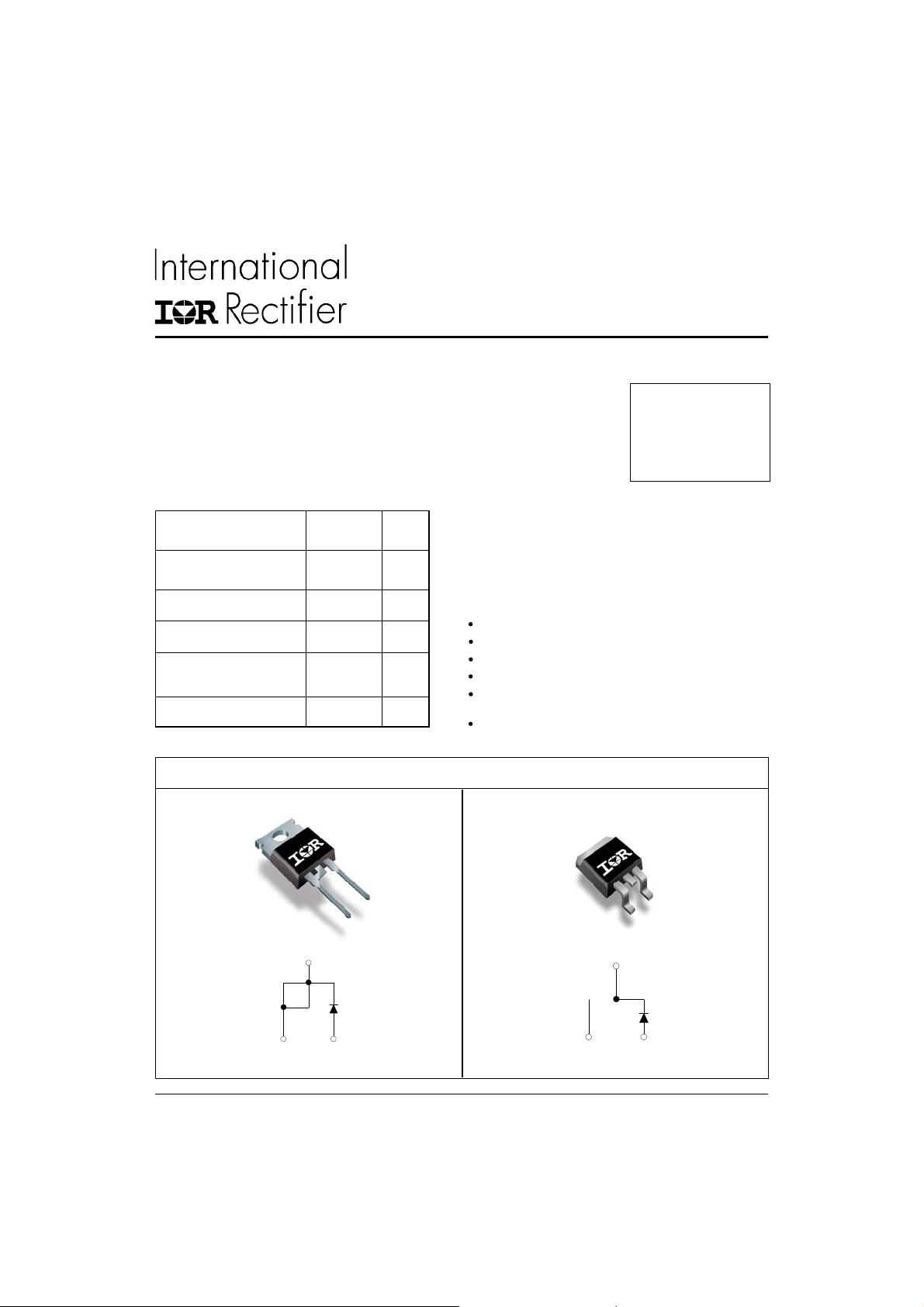
Case Styles
20L15TS
athode
Cathode
1
3
/C
Cathode
1
2
3
Anod
TO-220AC D2PAK
1www.irf.com
20L15T, 20L15TS
Bulletin PD-20577 rev. E 06/06
Voltage Ratings
Part number Values
V
Max. DC Reverse Voltage (V) @ T
R
V
Max. Working Peak Reverse Voltage (V) @ T
RWM
= 100 °C
J
= 100 °C
J
15
Absolute Maximum Ratings
Parameters Values Units Conditions
I
Max. Average Forward Current 20 A 50% duty cycle @ TC = 85°C, rectangular wave form
F(AV)
* See Fig. 5
I
Max. Peak One Cycle Non-Repetitive 700 5μs Sine or 3μs Rect. pulse
FSM
Surge Current * See Fig. 7 330 10ms Sine or 6ms Rect. pulse
EASNon-Repetitive Avalanche Energy 10 mJ T
A
= 25 °C, I
J
= 2 Amps, L = 6 mH
AS
IARRepetitive Avalanche Current 2 A Current decaying linearly to zero in 1 μsec
Frequency limited by TJ max. VA = 1.5 x VR typical
Following any rated
load condition and with
rated V
RRM
applied
Electrical Specifications
Parameters Values Units Conditions
Typ. Max.
VFMForward Voltage Drop - 0.41 V @ 19A
* See Fig. 1 (1) - 0.52 V @ 40A
0.25 0.33 V @ 19A
0.37 0.50 V @ 40A
IRMReverse Leakage Current - 10 mA TJ = 25 °C
* See Fig. 2 (1) - 600 mA TJ = 100 °C
V
Threshold Voltage 0.182 V T
F(TO)
J
= T
J
rtForward Slope Resistance 7.6 mΩ
CTMax. Junction Capacitance - 2000 pF VR = 5VDC, (test signal range 100Khz to 1Mhz) 25°C
LSTypical Series Inductance 8 - nH Measured lead to lead 5mm from package body
dv/dt Max. Voltage Rate of Change 10,000 V/ μs (Rated VR)
TJ = 25 °C
TJ = 125 °C
VR = rated V
R
max.
(1) Pulse Width < 300μs, Duty Cycle <2%
Thermal-Mechanical Specifications
Parameters Values Units Conditions
TJMax. Junction Temperature Range -55 to 125 °C
T
Max. Storage Temperature Range -55 to 150 °C
stg
R
Max. Thermal Resistance 1.5 °C/W DC operation * See Fig. 4
thJC
Junction to Case
R
Typical Thermal Resistance 0.50 °C/W Mounting surface , smooth and greased
thCS
Case to Heatsink For TO-220
R
Max. Thermal Resistance 40 °C/W DC operation
thJA
Junction to Ambient For D2Pak
wt Approximate Weight 2 (0.07) g (oz.)
T Mounting Torque Min. 6 (5) Non-lubricated threads
Max. 12 (10)
Kg-cm
(Ibf-in)
Marking Device 20L15T Case Style TO-220
20L15TS Case Style D2Pak
2
www.irf.com
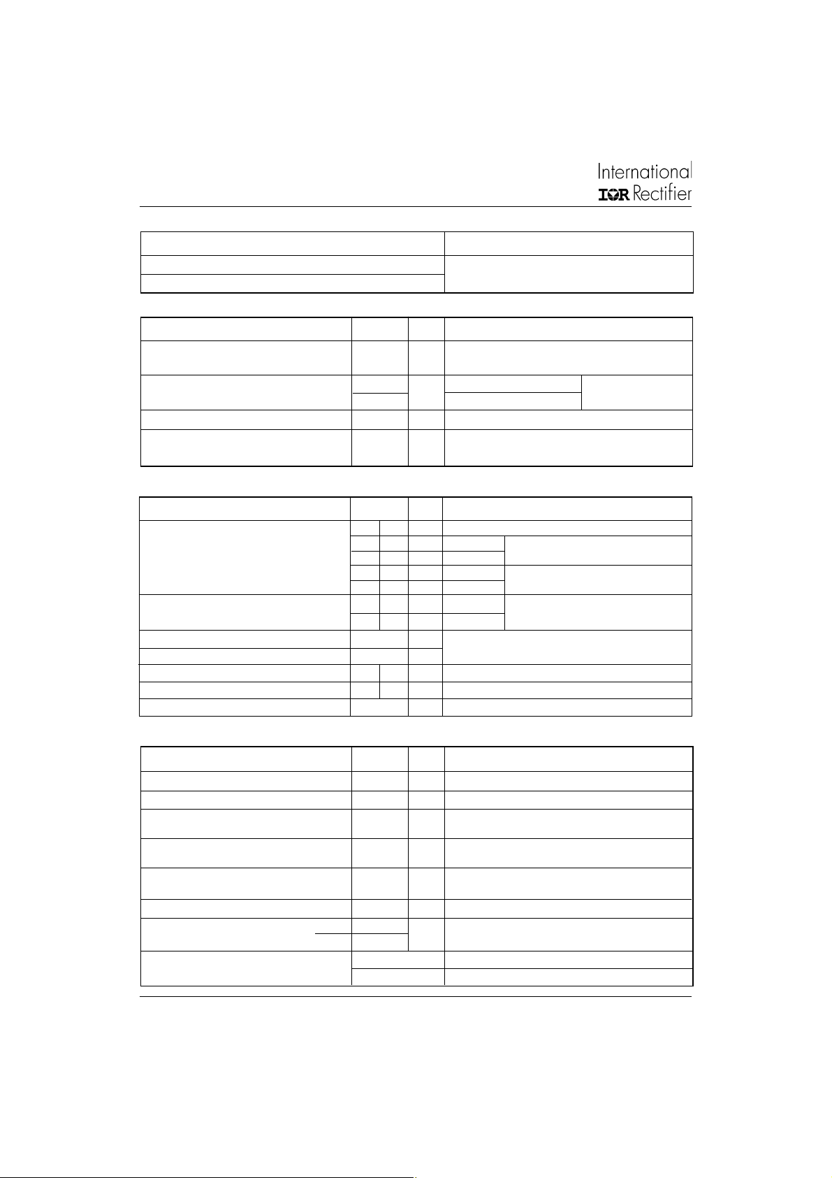
1000
20L15T, 20L15TS
Bulletin PD-20577 rev. E 06/06
1000
T = 100°C
J
100
R
75°C
100
F
T = 125°C
10
Instantaneous Forward Current - I (A)
1
0 0.2 0.4 0.6 0.8 1 1.2 1.4 1.6
Fo rwa rd Volta ge Dro p - V (V)
J
T = 75°C
J
T = 25°C
J
FM
Fig. 1 - Maximum Forward Voltage Drop Characteristics
10
10
50°C
25°C
1
Re verse Current - I (m A)
0.1
03691215
Reverse Voltage - V (V)
Fig. 2 - Typical Values of Reverse Current
Vs. Reverse Voltage
10000
T
T = 2 5 °C
J
1000
Junction Capa citanc e - C (pF)
100
0 5 10 15 20
Reverse Vo lta ge - V (V)
R
Fig. 3 - Typical Junction Capacitance
Vs. Reverse Voltage
R
Thermal Impedance Z (°C/W)
www.irf.com
thJC
D = 0.50
D = 0.33
D = 0.25
D = 0.20
0.1
Si n g l e P u l se
(Thermal Resistance)
Not es:
1. Duty f ac to r D = t / t
2. Pe ak T = P x Z + T
0.01
0.00001 0.0001 0.001 0.01 0.1 1 10 100
t , Rec ta ng ular Pulse Dura tio n (Se c o nds)
Fig. 4 - Maximum Thermal Impedance Z
1
thJC
P
DM
t
J
DM
Characteristics
1
t
2
1
thJC
D = 0.75
1
2
C
3
20L15T, 20L15TS
Bulletin PD-20577 rev. E 06/06
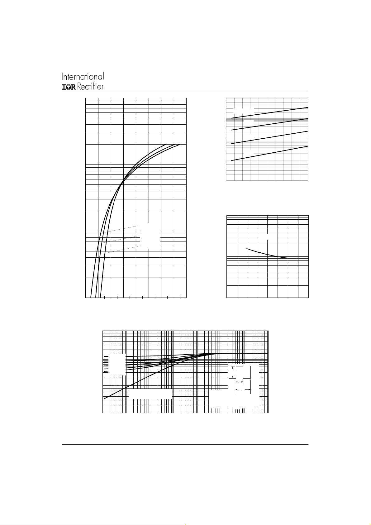
100
95
90
85
Sq uare wa ve (D = 0.50)
80
75
Allowable Case Temperature - (°C)
see note (2 )
70
0 4 8 12 16 20 24
Ave rag e Fo rward Current - I (A)
Fig. 5 - Maximum Allowable Case Temperature
Vs. Average Forward Current
1000
FSM
F( A V )
14
D = 0.20
D = 0.25
12
D = 0.33
D = 0.50
10
D = 0.75
RM S Li m i t
8
6
4
Average Power Loss - (Watts)
2
0
0 5 10 15 20 25 30
Ave rag e Fo rwa rd Current - I (A)
Fig. 6 - Forward Power Loss Characteristics
DC
F( A V )
CURRENT
MONITOR
(2) Formula used: T
Pd = Forward Power Loss = I
Pd
= Inverse Power Loss = VR1 x IR (1 - D); IR @ V
REV
4
DUT
= TJ - (Pd + Pd
C
At Any Rated Load Cond it io n
And With Rate d V Ap plied
Follow ing Surge
Non-Repe titive Surge Current - I (A)
100
10 100 1000 10000
Sq ua re Wa ve Pulse Duration - t (mic rose c )
RRM
p
Fig. 7 - Maximum Non-Repetitive Surge Current
L
IRFP46 0
Rg = 2 5 o h m
FREE- W H EEL
DIODE
40HFL40S02
Fig. 8 - Unclamped Inductive Test Circuit
) x R
thJC
;
F(AV)
/ D) (see Fig. 6);
= 80% rated V
R1
R
F(AV)
REV
x VFM @ (I
HIG H-SPEED
SWITCH
Vd = 25 Volt
+
www.irf.com
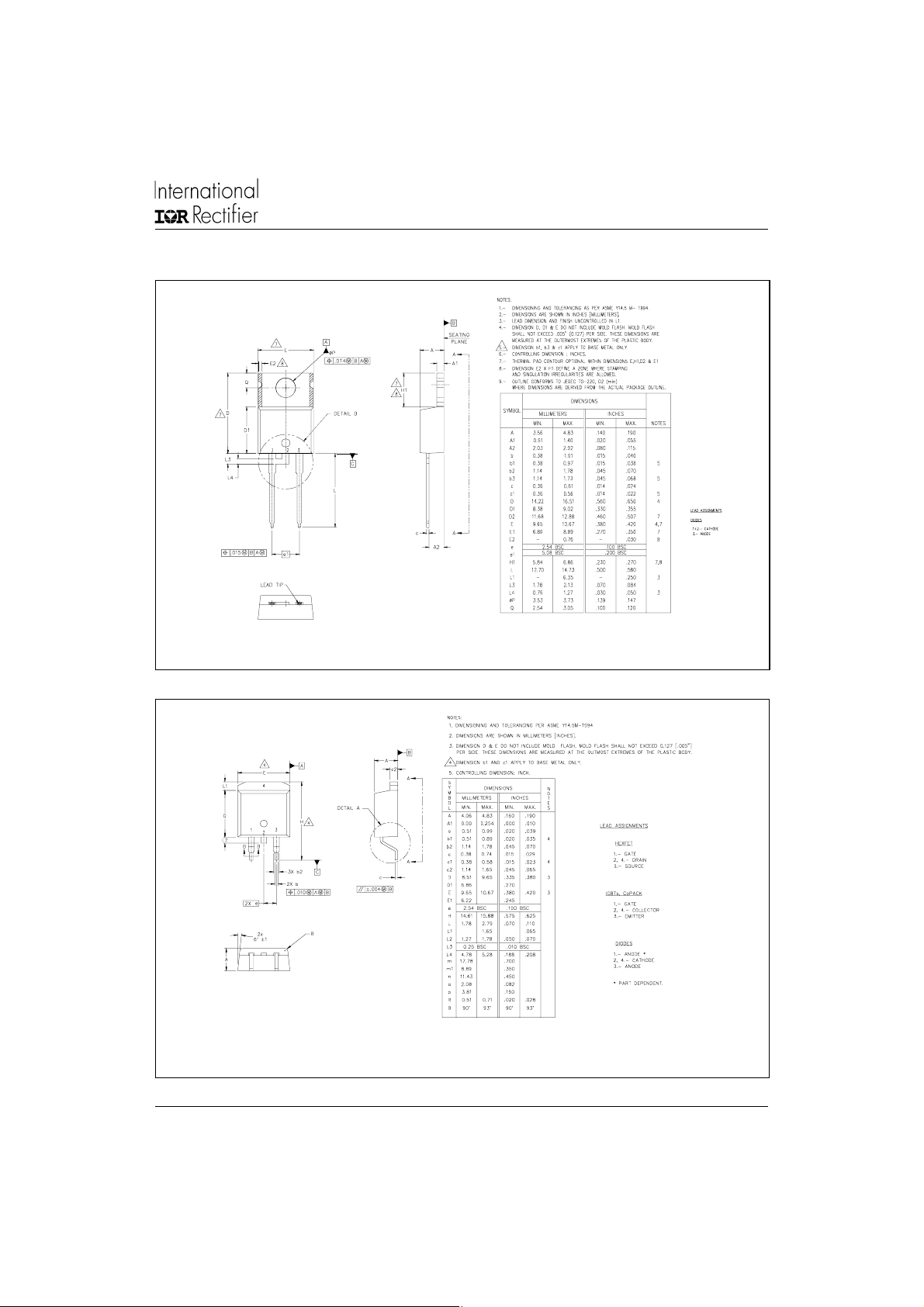
Outline Table
20L15T, 20L15TS
Bulletin PD-20577 rev. E 06/06
Conform to JEDEC outline TO-220AC
Dimensions in millimeters and (inches)
www.irf.com
Conform to JEDEC outline D2Pak (SMD-220)
Dimensions in millimeters and (inches)
5
20L15T, 20L15TS
Bulletin PD-20577 rev. E 06/06
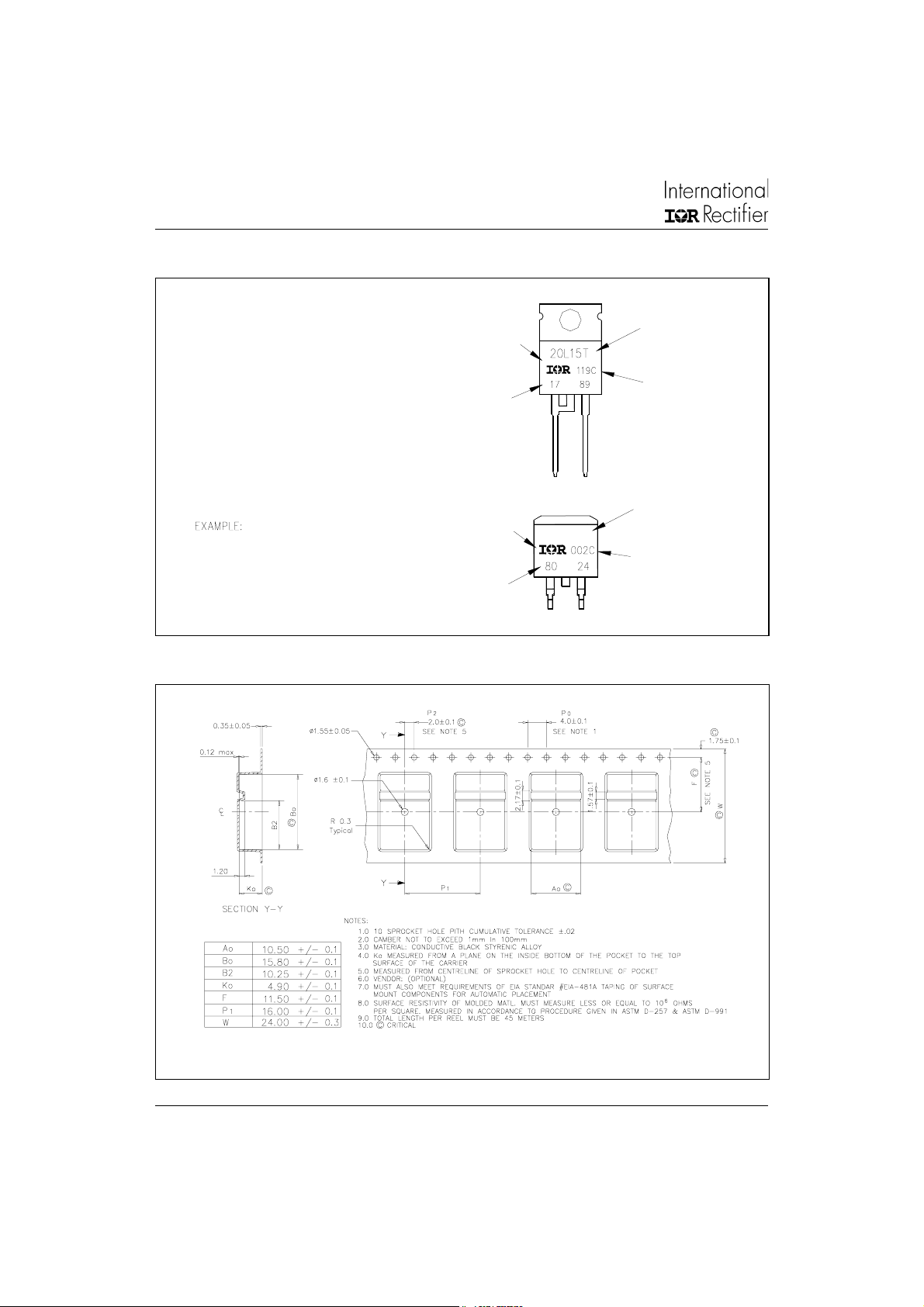
Part Marking Information
TO-220AC
EXAMPLE:
THIS IS A 20L15T
LOT CODE 1789
ASSEMBLED ON WW 19, 2001
IN THE ASSEMBLY LINE "C"
D2Pak
THIS IS A 20L15TS
LOT CODE 8024
ASSEMBLED ON WW 02, 2000
INTERNATIONAL
RECTIFIER
LOGO
ASSEMBLY
LOT CODE
INTERNATIONAL
RECTIFIER
LOGO
ASSEMBLY
LOT CODE
PART NUMBER
DATE CODE
YEAR 1 = 2001
WEEK 19
LINE C
PART NUMBER
20L15TS
DATE CODE
YEAR 0 = 2000
WEEK 02
LINE C
Tape & Reel Information
6
Dimensions in millimeters and (inches)
www.irf.com
Ordering Information Table
Device Code
20L15T, 20L15TS
Bulletin PD-20577 rev. E 06/06
20 L 15 T -
24
1
1 - Current Rating (20 = 20A)
2 - Schottky "L" Series
3 - Voltage Code (15 = 15V)
4 - Package
T = TO-220
5 - y none = Standard Production
3
5
y PbF = Lead-Free
Tube Standard Pack Quantity : 50 pieces
This product has been designed and qualified for Industrial Level.
Data and specifications subject to change without notice.
Qualification Standards can be found on IR's Web site.
IR WORLD HEADQUARTERS: 233 Kansas St., El Segundo, California 90245, USA Tel: (310) 252-7105
TAC Fax: (310) 252-7309
Visit us at www.irf.com for sales contact information. 06/06
www.irf.com
7
 Loading...