

Infineon SFH617A, SFH610A, SFH615A Datasheet
SFH610A/615A/617A
5.3 kV TRIOS Optocoupler
High Reliability
FEATURES
• High Current Transfer Ratios
at 10 mA: 40–320%
at 1.0 mA: 60% typical (>13)
• Low CTR Degradation
• Good CTR Linearity Depending on Forward Current
• Withstand Test Voltage, 5300 V
• High Collector-Emitter Voltage, V
RMS
CEO
=70 V
• Low Saturation Voltage
• Fast Switching Times
• Field-Effect Stable by TRIOS
(TRansparent IOn Shield)
• Temperature Stable
• Low Coupling Capacitance
• End-Stackable, .100" (2.54 mm) Spacing
• High Common-Mode Interference Immunity
(Unconnected Base)
• Underwriters Lab File #52744
V
DE
• VDE 0884 Available with Option 1
• SMD Option – See SFH6106/16/56 Data Sheet
DESCRIPTION
The SFH61XA features a high current transfer ratio, low
coupling capacitance and high isolation voltage. These
couplers have a GaAs infrared emitting diode emitter,
which is optically coupled to a silicon planar phototransistor detector, and is incorporated in a plastic DIP-4
package.
The coupling devices are designed for signal transmission
between two electrically separated circuits.
The couplers are end-stackable with 2.54 mm spacing.
Creepage and clearance distances of >8 mm are
achieved with option 6. This version complies with IEC 950
(DIN VDE 0805) for reinforced insulation up to an operation voltage of 400 V
Specifications subject to change.
RMS
or DC.
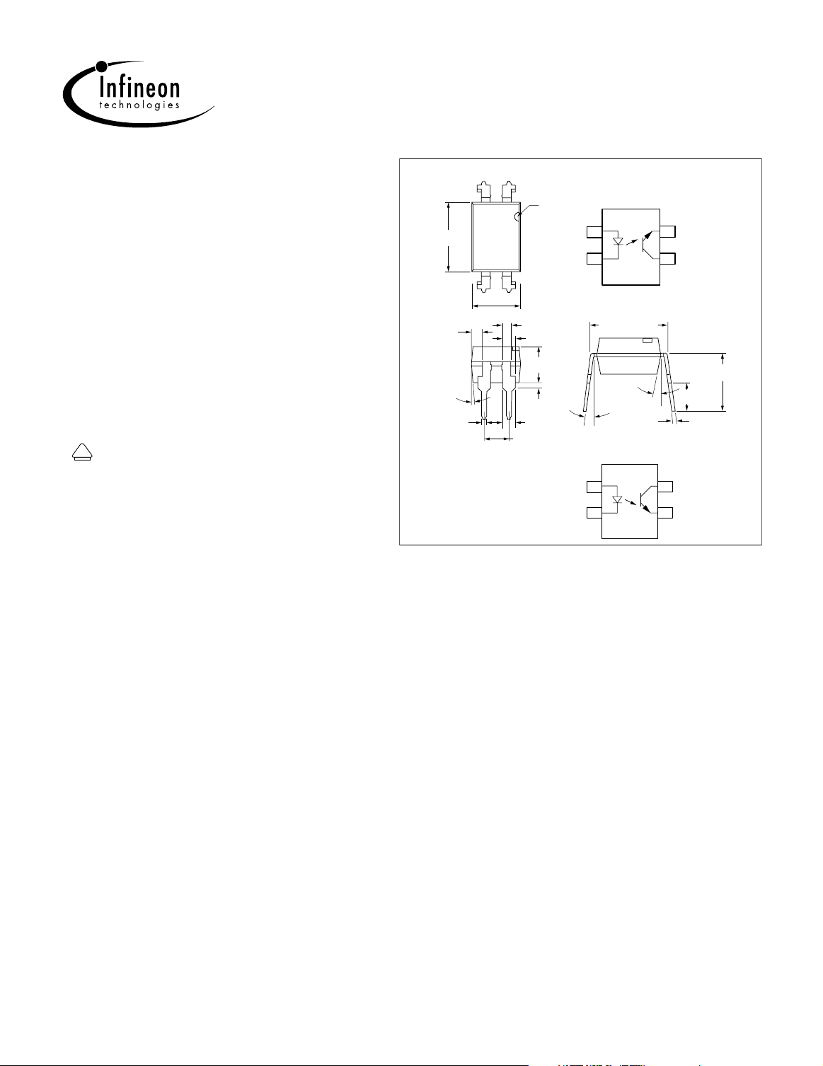
Dimensions in Inches (mm)
2
.255 (6.48)
.268 (6.81)
.030 (.76)
.045 (1.14)
4°
typ.
.018 (.46)
.022 (.56)
1
3
4
.179 (4.55)
.190 (4.83)
pin one ID
.031 (.79) typ.
.050 (1.27) typ.
.130 (3.30)
.150 (3.81)
.020 (.508 )
.035 (.89)
.050 (1.27)
1.00 (2.54)
Cathode
Anode
Cathode
Anode
SFH610A
1
2
.300 (7.62) typ.
10°
3°–9°
.008 (.20)
.012 (.30)
SFH615A/617A
1
2
Emitter
4
3
Collector
.110 (2.79)
.130 (3.30)
Collector
4
3
Emitter
.230 (5.84)
.250 (6.35)
Maximum Ratings
Emitter
Reverse Voltage............................................................................6 V
DC Forward Current.................................................................60 mA
Surge Forward Current (tP≤10 µs).............................................2.5 A
Total Power Dissipation.........................................................100 mW
Detector
Collector-Emitter Voltage ............................................................70 V
Emitter-Collector Voltage ..............................................................7 V
Collector Current .....................................................................50 mA
Collector Current (t
≤
1 ms)....................................................100 mA
P
Total Power Dissipation.........................................................150 mW
Package
Isolation Test Voltage between Emitter and Detector,
refer to Climate DIN 40046, part 2, Nov. 74................. 5300 V
RMS
Creepage................................................................................≥7 mm
Clearance ...............................................................................≥7 mm
Insulation Thickness between Emitter and Detector ...........≥0.4 mm
Comparative Tracking Index
per DIN IEC 112/VDE0 303, part 1 ........................................≥175
Isolation Resistance
V
=500 V, TA=25°C..........................................................≥1012
IO
VIO=500 V, TA=100°C........................................................≥1011
Storage Temperature Range ......................................–55 to +150°C
Ambient Temperature Range......................................–55 to +100°C
Junction Temperature ..............................................................100°C
Soldering Temperature (max. 10 s. Dip Soldering
Distance to Seating Plane ≥1.5 mm)....................................260°C
Ω
Ω
Infineon Technologies, Corp. • Optoelectronics Division • Cupertino, CA (formerly Siemens Microelectronics, Inc.)
www.infineon.com/opto • 1-800-777-4363 1 November 23, 1999–15
Characteristics
(TA=25°C)
Description Symbol Unit Condition
Emitter (IR GaAs)
Forward Voltage V
Reverse Current I
Capacitance C
Thermal Resistance R
F
R
0
thJA
1.25 (≤1.65) V IF=60 mA
0.01 (≤10)
µ
AVR=6 V
13 pF VR=0 V, f=1 MHz
750 K/W
Detector (Si Phototransistor)
Capacitance C
Thermal Resistance R
CE
thJA
5.2 pF VCE=5 V, f=1 MHz
500 K/W
Package
Collector-Emitter Saturation Voltage V
Coupling Capacitance C
Current Transfer Ratio
(IC/IF at VCE=5 V)
CESAT
C
and Collector-Emitter Leakage Current by Dash Number
0.25 (≤0.4) V IF=10 mA, IC=2.5 mA
0.4 pF
Description -1 -2 -3 -4
IC/ IF (IF=10 mA) 40–80 63–125 100–200 160–320 %
/ IF (IF=1 mA) 30 (>13) 45 (>22) 70 (>34) 90 (>56)
I
C
2 (
≤
Collector-Emitter Leakage Current, I
VCE=10 V
Switching Times (Typical)
Linear Operation
I
F
47 Ω
Switching Operation
(without saturation)
RL=75 Ω
I
C
(with saturation)
CEO
=5 V
V
CC
50) 2 (≤50) 5 (≤100) 5 (≤100) nA
IF=10 mA, VCC=5 V, TA=25°C
Load Resistance R
Turn-on Time t
Rise Time t
Turn-off Time t
Fall Time t
Cut-off Frequency F
L
ON
R
OFF
F
CO
75
Ω
3.0 µs
2.0
2.3
2.0
250 kHz
I
F
1 KΩ
=5 V
V
CC
Parameter Sym.
-1
IF=20 mA
47 Ω
Rise Time t
Turn-off Time t
Fall Time t
Infineon Technologies, Corp. • Optoelectronics Division • Cupertino, CA (formerly Siemens Microelectronics, Inc.)
www.infineon.com/opto • 1-800-777-4363 2 November 23, 1999–15
Turn-on Time t
ON
R
OFF
F
3.0 4.2 6.0 µs
2.0 3.0 4.6
18 23 25
11 14 15
Dash No.
-2 and -3
IF=10 mA-4IF=5 mA
Unit
SFH610/11/15/17A
 Loading...