

INVT CHF100A-004G-2, CHF100A-0R7G-2, CHF100A-7R5G-2, CHF100A-5R5G-2, CHF100A-2R2G-S2 Operation Manual
...

CHF100A series high performance universal inverter
TABLE OF CONTENTS
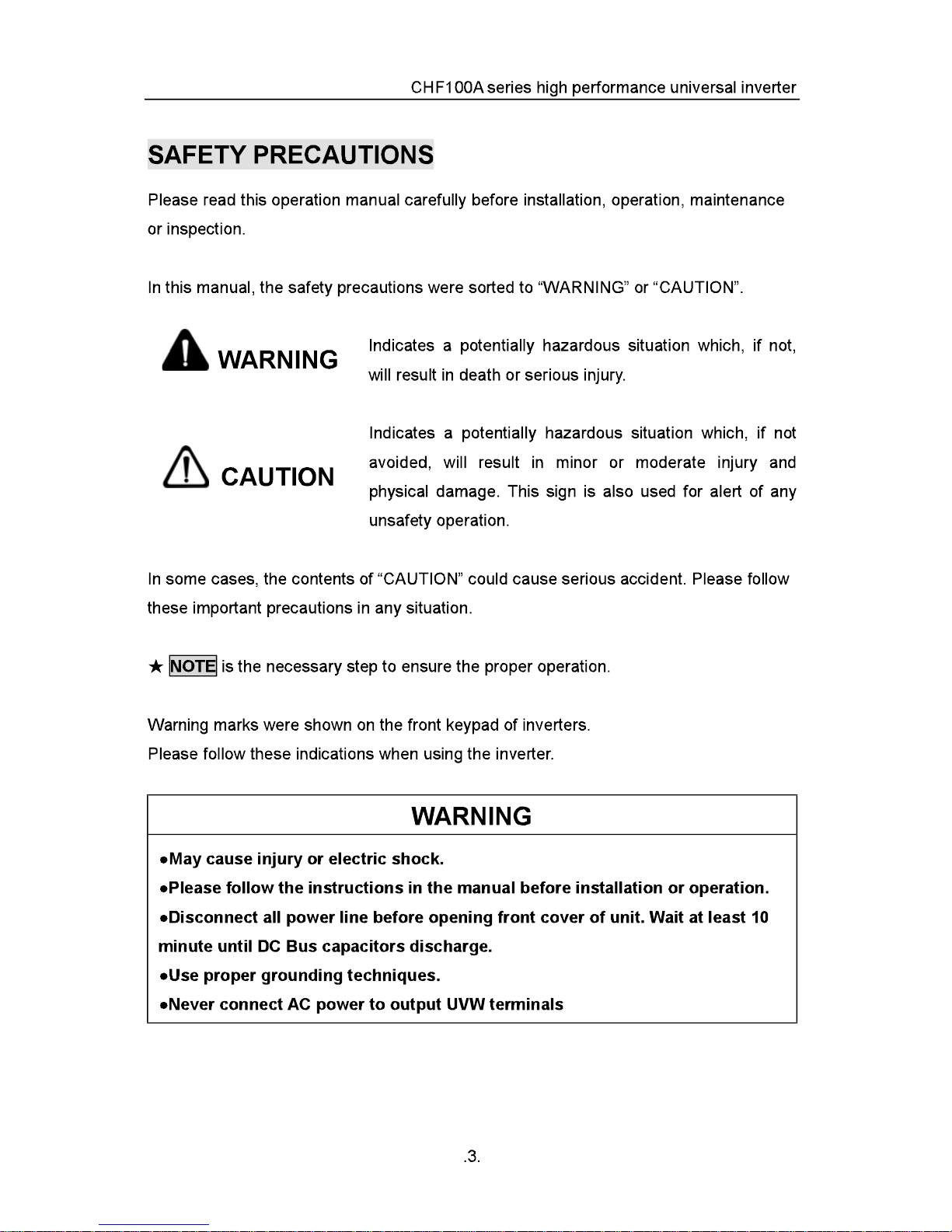
SAFETY PRECAUTIONS........................................................................................3
1. INTRODUCTION...............................................................................................4
1.1 Technology Features..................................................................................4
1.2 Description of Name Plate..........................................................................5
1.3 Selection Guide..........................................................................................5
1.4 Parts Description........................................................................................7
2. UNPACKING INSPECTION.................................................................................9
3. INSTALLATION..............................................................................................10
3.1 Environmental Requirement.....................................................................11
4. WIRING...........................................................................................................12
4.1 Connection of Peripheral Devices............................................................13
4.2 Terminal Configuration..............................................................................14
4.3 Wiring Diagram.........................................................................................16
4.4 Wiring Main Circuits..................................................................................18
4.5 Wiring Control Circuit................................................................................21
4.6 Installation Guidline to EMC Compliance..................................................23
5. OPERATION......................................................................................................27
5.1 Keypad Description..................................................................................27
5.2 Operation Process....................................................................................29
5.3 Running State...........................................................................................31
5.4 Shortcut Menu..........................................................................................32
6. DETAILED FUNCTION DESCRIPTION.............................................................33
6.1 P0 Group--Basic Function........................................................................33
6.2 P1 Group --Start and Stop Control............................................................41
6.3 P2 Group--Motor Parameters...................................................................46
6.4 P3 Group—Vector Control........................................................................47
6.5 P4 Group—V/F Control............................................................................50
6.6 P5 Group--Input Terminals........................................................................54
6.7 P6 Group--Output Terminals.....................................................................61
6.8 P7 Group—Display Interface....................................................................66
6.9 P8 Group--Enhanced Function.................................................................72
6.10 P9 Group--PID Control...........................................................................78
6.11 PA Group--Simple PLC and Multi-step Speed Control.............................82
.1.

CHF100A series high performance universal inverter
6.12 PB Group-- Protection Function..............................................................88
6.13 PC Group--Serial Communication..........................................................93
6.14 PD Group--Supplementary Function.......................................................95
6.15 PE Group—Factory Setting....................................................................96
7. TROUBLE SHOOTING.....................................................................................97
7.1 Fault and Trouble shooting.......................................................................97
7.2 Common Faults and Solutions................................................................100
8. MAINTENANCE..........................................................................................102
8.1 Daily Maintenance..................................................................................102
8.2 Periodic Maintenance.............................................................................103
8.3 Replacement of wearing parts................................................................104
9. COMMUNICATION PROTOCOL.....................................................................105
9.1 Interfaces...............................................................................................105
9.2 Communication Modes...........................................................................105
9.3 Protocol Format......................................................................................105
9.4 Protocol function.....................................................................................106
9.5 Note:........................................................................................................111
9.6 CRC Check.............................................................................................111
9.7 Example..................................................................................................111
Appendix A: External Dimension......................................................................113
A.1 380V.......................................................................................................113
A.2 220V.......................................................................................................115
A.3 Installation Space....................................................................................117
A.4 Dimensions of External small Keypad.....................................................117
A.5 Dimensions of External big Keypad.........................................................118
A.6 Disassembly............................................................................................118
Appendix B Specifications of Breaker, Cable, Contactor and Reactor..........121
B.1 Specifications of breaker, cable and contactor.......................................121
B.2 Specifications of AC input/output reactor and DC reactor.......................122
B.3 Specifications of AC input/output filter....................................................123
B.4 Specifications of braking unit and braking resistor..................................124
Appredix C: LIST OF FUNCTION PARAMETERS.............................................128
.2.

CHF100A series high performance universal inverter
1. INTRODUCTION
1.1 Technology Features
● Input & Output
u Input Voltage Range: 380/220V±15%
u Input Frequency Range: 47~63Hz
u Output Voltage Range: 0~rated input voltage
u Output Frequency Range: 0~400Hz
● I/O Features
u Programmable Digital Input: Provide 7 terminals which can support ON-OFF
inputs, 1 terminal which can support high speed pulse input and support PNP,
NPN
u Programmable Analog Input: AI1 can accept input of -10V ~10V, AI2 can accept
input of 0~10V or 0~20mA.
u Programmable Open Collector Output: Provide 1 output terminal (open collector
output)
u Relay Output: Provide 2 output terminals
u Analog Output: Provide 2 output terminal, whose output scope can be 0/4~20 mA
or 0~10 V, as chosen.
● Main Control Function
u Control Mode: V/F control, Sensorless Vector Control (SVC)
u Overload Capacity: 60s with 150% of rated current, 10s with 180% of rated
current.
u Speed Adjusting Range: 1:100 (SVC)
u Carrier Frequency: 1 kHz ~15.0 kHz.
u Frequency reference source: keypad, analog input, HDI, serial communication,
multi-step speed, simple PLC and PID. The combination of multi- modes and the
switch between different modes can be realized.
u PID Control Function
u Simple PLC, Multi-Steps Speed Control Function: 16 steps speed can be set.
u Traverse Control Function
u None-Stop when instantaneous power off.
u Speed Trace Function: Smoothly start the running motor.
u QUICK/JOG Key: User defined shortcut key can be realized.
u Automatic Voltage Regulation Function (AVR):
.4.
CHF100A series high performance universal inverter
u Automatically keep the output voltage stable when input voltage fluctuating
u Up to 25 fault protections:
u Protect from over current, over voltage, under voltage, over temperature, phase
failure, over load etc.
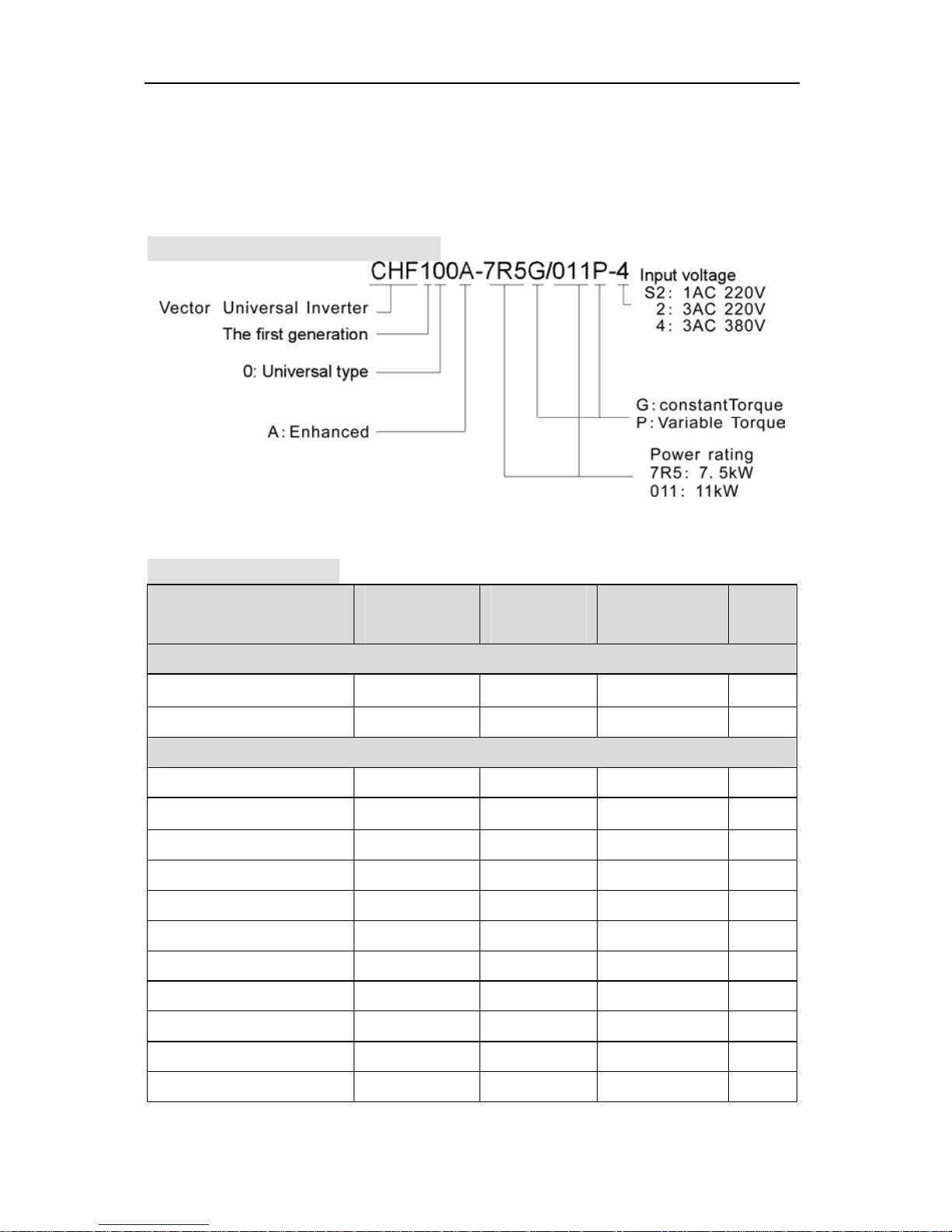
1.2 Description of Name Plate
Figure 1.1 Nameplate of inverter.
1.3 Selection Guide
Model No.
Rated output
Power (kW)
1AC 220V ±15%
CHF100A-1R5G-S2 1.5 14.2 7.0 B
CHF100A-2R2G-S2 2.2 23.0 10 B
3AC 220V ±15%
CHF100A-0R7G-2 0.75 5.0 4.5 B
CHF100A-1R5G-2 1.5 7.7 7 B
CHF100A-2R2G-2 2.2 11.0 10 B
CHF100A-004G-2 4.0 17.0 16 C
CHF100A-5R5G-2 5.5 21.0 20 C
CHF100A-7R5G-2 7.5 31.0 30 D
CHF100A-011G-2 11.0 43.0 42 E
Rated input
current (A)
Rated output
current (A)
Size
CHF100A-015G-2 15.0 56.0 55 E
CHF100A-018G-2 18.5 71.0 70 E
CHF100A-022G-2 22.0 81.0 80 F
CHF100A-030G-2 30.0 112.0 110 F
.5.

CHF100A series high performance universal inverter
Rated output
Rated input
Rated output
Model No.
Power (kW)
current (A)
current (A)
CHF100A-037G-2 37.0 132.0 130 F
CHF100A-045G-2 45.0 163.0 160 G
CHF100A-055G-2 55.0 181.0 190.0 G
3AC 380V ±15%
CHF100A-1R5G/2R2P-4
CHF100A-2R2G/004P-4
CHF100A-004G/5R5P-4
CHF100A-5R5G/7R5P-4
CHF100A-7R5G/011P-4
CHF100A-011G/015P-4
CHF100A-015G/018P-4
CHF100A-018G/022P-4
CHF100A-022G/030P-4
1.5 5.0 3.7 B
2.2 5.8 5 B
4.0/5.5 10/15 9/13 C
5.5/7.5 15/20 13/17 C
7.5/11 20/26 17/25 D
11/15 26/35 25/32 D
15/ 18.5 35/38 32/37 D
18.5/ 22 38/46 37/45 E
22/30 46/62 45/60 E
Size
CHF100A-030G/037P-4
CHF100A-037G/045P-4
CHF100A-045G/055P-4
CHF100A-055G/075P-4
CHF100A-075G/090P-4
CHF100A-090G/110P-4
CHF100A-110G/132P-4
CHF100A-132G/160P-4
CHF100A-160G/185P-4
CHF100A-185G/200P-4
CHF100A-200G/220P-4
CHF100A-220G/250P-4
CHF100A-250G/280P-4
CHF100A-280G/315P-4
CHF100A-315G/350P-4
30/37 62/76 60/75 E
37/45 76/90 75/90 F
45/55 90/105 90/110 F
55/75 105/ 140 110/ 150 F
75/90 140/ 160 150/ 176 G
90/110 160/ 210 176/ 210 G
110/132 210/ 240 210/ 250 G
132/160 240/ 290 250/ 300 H
160/185 290/ 330 300/ 340 H
185/200 330/ 370 340/ 380 H
200/220 370/ 410 380/ 415 I
220/250 410/ 460 415/ 470 I
250/280 460/ 500 470/ 520 I
280/315 500/ 580 520/ 600 I
315/350 580/ 620 600/ 640 I
CHF100A-350G-4 350 620 640 2*H
CHF100A-400G-4 400 670 690 2*I
CHF100A-500G-4 500 835 860 2*I
CHF100A-560G-4 560 920 950 2*I
.6.

CHF100A series high performance universal inverter
1.4 Parts Description
Figure 1.2 Parts of inverter (15kw and below).
.7.

CHF100A series high performance universal inverter
Figure 1.3 Parts of inverter (18.5kw and above).
.8.


CHF100A series high performance universal inverter
(m)
3.1 Environmental Requirement
3.1.1 Temperature
Environment temperature range: -10°C ~ +40°C. Inverter will be derated at 4%/1°C if
ambient temperature exceeds 40°C up to 50°C. The utmost permited ambient
temperature shoud not exceed 50°C.
3.1.2 Humidity
Less than 90% RH, without dewfall.
3.1.3 Altitude
Inverter can output the rated power when installed with altitude of lower than 1000m. It
will be derated when the altitude is higher than 1000m. For details, please refer to the
following figure:
Iout
100%
80%
60%
40%
20%
1000 2000 3000 4000
Figure 3.1 Relationship between output current and altitude.
3.1.4 Impact and Oscillation
It is not allowed that the inverter falls down or suffers from fierce impact or the inverter is
installed at the place that oscillation frequently.
3.1.5 Electromagnetic Radiation
Keep away from the electromagnetic radiation source.
3.1.6 Water
Do not install the inverter at the wringing or dewfall place.
3.1.7 Air Pollution
Keep away from air pollution such as dusty, corrosive gas.
3.1.8 Storage
Do not store the inverter in the environment with direct sunlight, vapor, oil fog and
vibration.
.11.


CHF100A series high performance universal inverter
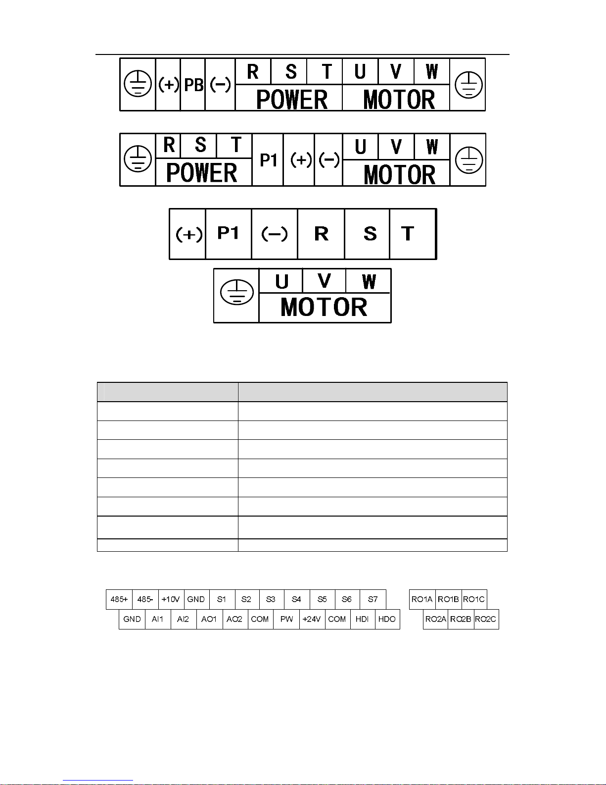
PB
P1
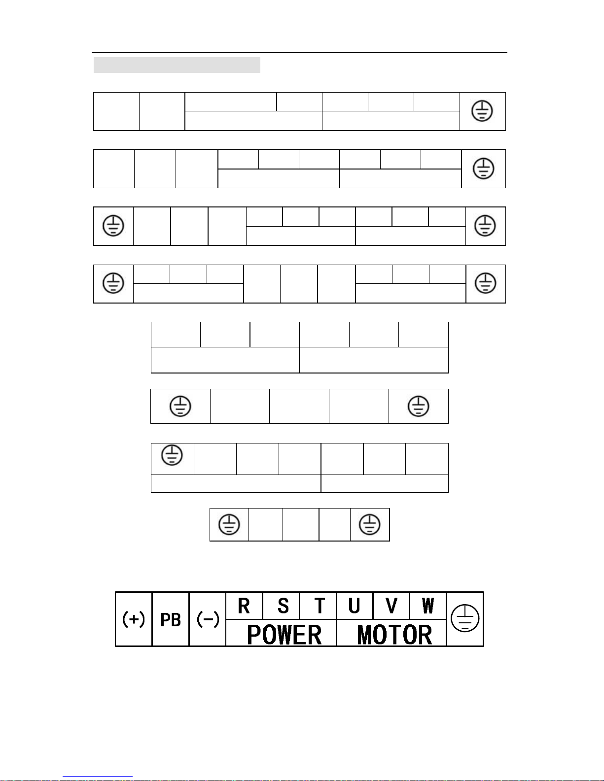
4.2 Terminal Configuration
4.2.1 Main Circuit Terminals (380VAC)
(+) PB
(+) PB (-)
(+)
R S T U V W
POWER
R S T U V W
R S T U V W
POWER MOTOR
Figure 4.2 Main circuit terminals (1.5~2.2kW).
R S T U V W
POWER MOTOR
Figure 4.3 Main circuit terminals (4~5.5kW).
R S T U V W
(-)
POWER MOTOR
Figure 4.4 Main circuit terminals (7.5~15kW).
P1
(+)
(-)
MOTOR
Figure 4.5 Main circuit terminals (18.5~110kW).
POWER MOTOR
Figure 4.6 Main circuit terminals (132~315kW).
P1 (+) (-)
R S T U V W
POWER MOTOR
Figure 4.7 Main circuit terminals (350~500kW).
4.2.2 Main Circuit Terminals (220VAC)
Figure 4.8 Main circuit terminals (4~5.5kW).
(+) (-)
.14.
CHF100A series high performance universal inverter
.15.
Figure 4.9 Main circuit terminals (7.5kW).
Figure 4.10 Main circuit terminals (11~18.5kW).
Figure 4.11 Main circuit terminals (22kW and bigger).
the main circuit terminals’s description are as following. Wire the terminal correctly for
the desired purposes.
Terminal Symbol Function Description
R、S、T Terminals of 3 phase AC input
(+)、(-) Spare terminals of external braking unit
(+)、PB Spare terminals of external braking resistor
P1、(+) Spare terminals of external DC reactor
(-) Terminal of negative DC bus
U、V、W Terminals of 3 phase AC output
Terminal of ground
(+) Terminal of positive DC bus
4.2.3 Control Circuit Terminals
Figure 4.12 Control circuit terminals.
CHF100A series high performance universal inverter
.16.
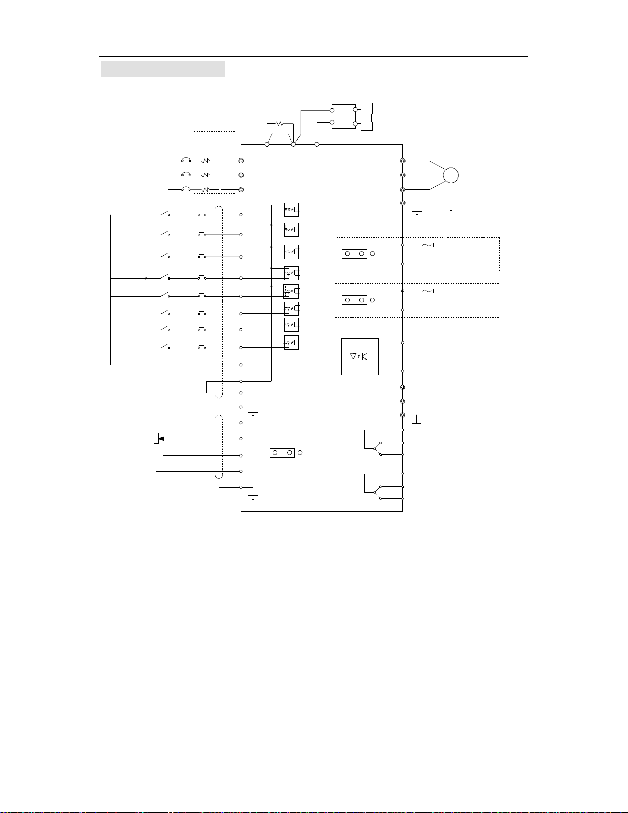
4.3 Wiring Diagram
4.3.1 Typical Wiring Diagram
Multifunctional On-Off Input 1
Multifunctional On-Off Input 2
Multifunctional On-Off Input 3
+24V
0-10V/0-20mA
Analog Output
J17
V I
Jumper of AI2 to select
I or V
J16
IV
0/4-20mA Input
0-10V Input
Frequency/PID Setting
Multifunctional On-Off Input 4
AO2
GND
485 Communication selection
485+
485-485-
485+
Relay Output 1
PE
GND
AI2
AI1 Multifunctional Analog Input
Power Supply For Frequecy Setting
PE
COM
S4
S3
S2
S1
Propositional Protection
Circuit
R
S
T
W
V
U
PE
M
CHF100A Series
Inverter
P1 (+)
(-)
P
N
P
PB
Braking Resistor
DC Reactor
3 Phase
380V±15%
50/60Hz
RO1B
RO1C
{
RO2C
RO2B
RO2A
{
Relay Output 2
HD1
COM
HDOHigh Speed Pulse Input
Or Collector Open-circuit
Input
Collector Open-circuit Output
PW
S5
S6
S7
Multifunctional On-Off Input 5
Multifunctional On-Off Input 6
Multifunctional On-Off Input 7
0-10V/0-20mA
Analog Output
J15
V I
AO1
GND
RO1A
RO2B
Figure4.13 Typical Wiring diagram.
Notice:
u Inverters between 18.5kW and 90kW have built-in DC reactor which is used to
improve power factor. For inverters above 110kW, it is recommended to
install DC reactor between P1 and (+).
u The inverters below 18.5kW have build-in braking unit. If need braking, only
need to install braking resistor between PB and (+).
u For inverters above (including) 18.5kW, if need braking, should install
external braking unit between (+) and (-).
u Only the inverters above 4 kW provide Relay output 2.
u +24V connect with PW as default setting. If user need external power supply,
CHF100A series high performance universal inverter
public point
)
inner power
public point
)
exterior power
disconnect +24V with PW and connect PW with external power supply.
u 485+ and 485- are optional for 485 communications.
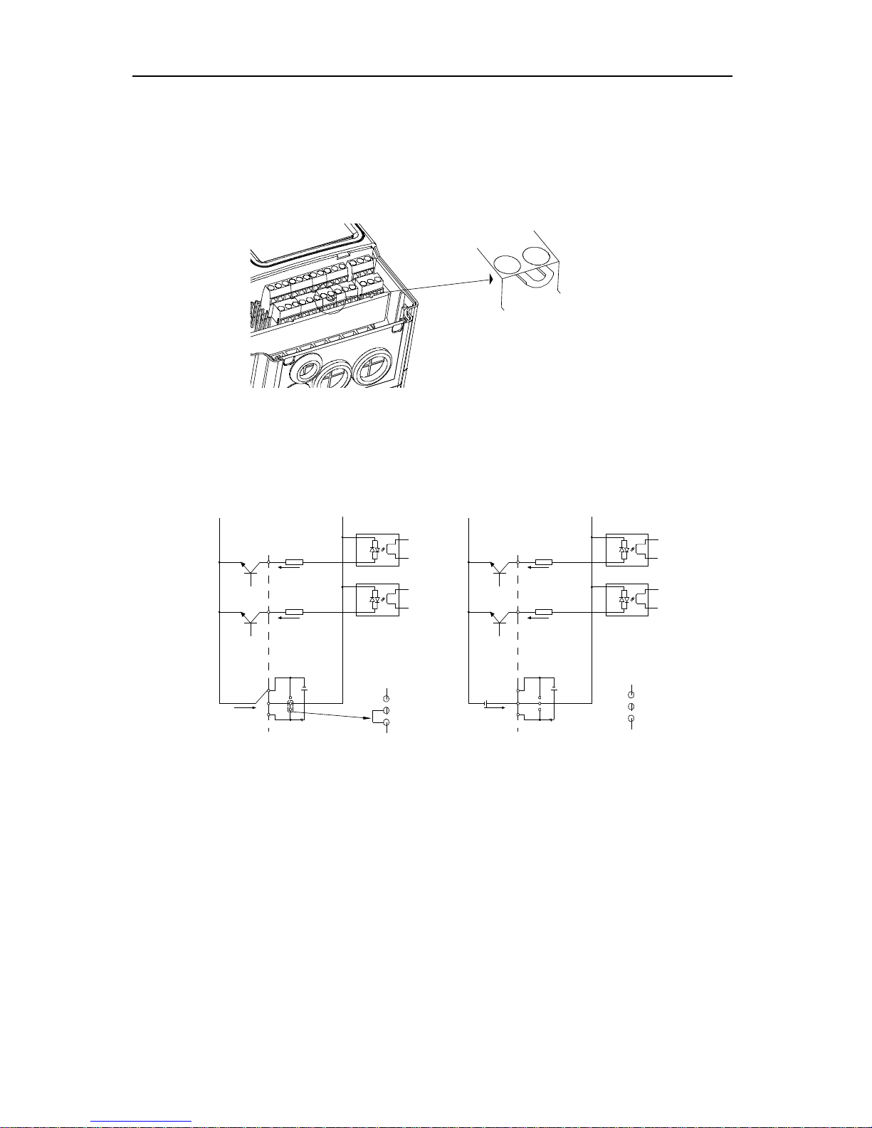
4.3.2 Outpu and input signal connection
Set the common emitter/common collector mode and out/input power supply by U-short
splicing. The factory setting is the common emitter.
Figure 4.14 U-short splicing.
Common emitter mode:
Please set the U-short splicing according to the type of power supply, when the input
signal is from the NPN transistor.
S1
S2
COM
+24V
COM
COM
PW
PW
+24V
+24V
Mode of common emitter( 0V is
COM
PW
+24V
S1
S2
COM
+24V
COM
COM
+24V
PW
PW
+24V
+24V
Mode of common emitter(0V is
COM
PW
+24V
Figure 4.15 Common emitter mode.
Common Collector mode:
Please set the U-short splicing according to the type of power supply, when the input
signal is from the PNP transistor.
.17.

CHF100A series high performance universal inverter
S1
S2
COM
+24V
COM
COM
PW
PW
+24V
+24V
Mode of common collector(+24V
is public point)inner power
COM
PW
+24V
S1
S2
COM
+24V
COM
COM
+24V
Mode of common collector(+24V is
public point)exterior power
PW
PW
+24V
+24V
COM
PW
+24V
Figure 4.16 Common collector mode.
4.4 Wiring Main Circuits
4.4.1 Wiring at input side of main circuit
4.4.1.1 Circuit breaker
It is necessary to connect a circuit breaker which is compatible with the capacity of
inverter between 3ph AC power supply and power input terminals (R, S, T ). The
capacity of breaker is 1.5~2 times to the rated current of inverter. For details, see
<Specifications of Breaker, Cable, and Contactor>.
4.4.1.2 Contactor
In order to cut off the input power effectively when something is wrong in the system,
contactor should be installed at the input side to control the ON-OFF of the main circuit
power supply.
4.4.1.3 AC reactor
In order to prevent the rectifier damage result from the large current, AC reactor should
be installed at the input side. It can also prevent rectifier from sudden variation of power
voltage or harmonic generated by phase-control load.
4.4.1.4 Input EMC filter
The surrounding device may be disturbed by the cables when the inverter is working.
EMC filter can minimize the interference. Just like the following figure.
.18.

CHF100A series high performance universal inverter
Figure4.17 Wiring at input side.
4.4.2 Wiring at inverter side of main circuit
4.4.2.1 DC reactor
Inverters from 18.5kW to 90kW have built-in DC reactor which can improve the power
factor,
4.4.2.2 Braking unit and braking resistor
• Inverter of 15KW and below have built-in braking unit. In order to dissipate the
regenerative energy generated by dynamic braking, the braking resistor should be
installed at (+) and PB terminals. The wire length of the braking resistor should be less
than 5m.
• Inverter of 18.5KW and above need connect external braking unit which should be
installed at (+) and (-) terminals. The cable between inverter and braking unit should be
less than 5m. The cable between braking unit and braking resistor should be less than
10m.
• The temperature of braking resistor will increase because the regenerative energy will
be transformed to heat. Safety protection and good ventilation is recommended.
Notice: Be sure that the electric polarity of (+) (-) terminals is right; it is not allowed
to connect (+) with (-) terminals directly, Otherwise damage or fire may occur.
4.4.3 Wiring at motor side of main circuit
4.4.3.1 Output Reactor
Output reator must be installed in the following condition. When the distance between
inverter and motor is more than 50m, inverter may be tripped by over-current protection
frequently because of the large leakage current resulted from the parasitic capacitance
with ground. And the same time to avoid the damage of motor insulation, the output
reactor should be installed.
4.4.3.2 Output EMC filter
.19.
CHF100A series high performance universal inverter
EMC filter should be installed to minimize the leakage current caused by the cable and
minimize the radio noise caused by the cables between the inverter and cable. Just see
the following figure.
Figure 4.18 Wiring at motor side.
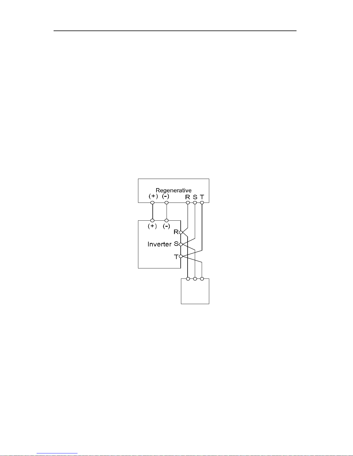
4.4.4 Wiring of regenerative unit
Regenerative unit is used for putting the electricity generated by braking of motor to the
grid. Compared with traditional 3 phase inverse parallel bridge type rectifier unit,
regenerative unit uses IGBT so that the total harmonic distortion (THD) is less than 4%.
Regenerative unit is widely used for centrifugal and hoisting equipment.
SR T
Grid
Figure 4.19 Wiring of regenerative unit.
4.4.5 Wiring of Common DC bus
Common DC bus method is widely used in the paper industry and chemical fiber industry
which need multi-motor to coordinate. In these applications, some motors are in driving
status while some others are in regenerative braking (generating electricity) status. The
regenerated energy is automatically balanced through the common DC bus, which
means it can supply to motors in driving status. Therefore the power consumption of
whole system will be less compared with the traditional method (one inverter drives one
motor).
.20.

CHF100A series high performance universal inverter
When two motors are running at the same time (i.e. winding application), one is in driving
status and the other is in regenerative status. In this case the DC buses of these two
inverters can be connected in parallel so that the regenerated energy can be supplied to
motors in driving status whenever it needs. Its detailed wiring is shown in the following
figure:
Figure 4.20 Wiring of common DC bus.
Notice: Two inverters must be the same model when connected with Common DC
bus method. Be sure they are powered on at the same time.
4.4.6 Ground Wiring (PE)
In order to ensure safety and prevent electrical shock and fire, terminal PE must be
grounded with ground resistance. The ground wire should be big and short, and it is
better to use copper wire (>3.5mm2). When multiple inverters need to be grounded, do
not loop the ground wire.
4.5 Wiring Control Circuit
4.5.1 Precautions
4.5.1.1 Use shielded or twisted-pair cables to connect control terminals.
4.5.1.2 Connect the ground terminal (PE) with shield wire.
4.5.1.3 The cable connected to the control terminal should leave away from the main
circuit and heavy current circuits (including power supply cable, motor cable, relay and
contactor connecting cable) at least 20cm and parallel wiring should be avoided. It is
suggested to apply perpendicular wiring to prevent inverter malfunction caused by
external interference.
.21.

CHF100A series high performance universal inverter
.22.
4.5.2 Control circuit terminals
Terminal Description
S1~S7
ON-OFF signal input, optical coupling with PW and COM.
Input voltage range: 9~30V
Input impedance: 3.3kΩ
HDI
High speed pulse or ON-OFF signal input, optical coupling with PW
and COM.
Pulse input frequency range: 0~50kHz
Input voltage range: 9~30V
Input impedance: 1.1kΩ
PW
External power supply. +24V terminal is connected to PW terminal
as default setting. If user need external power supply, disconnect
+24V terminal with PW terminal and connect PW terminal with
external power supply.
+24V
Provide output power supply of +24V.
Maximum output current: 150mA
AI1
Analog input, -10V~10V
Input impedance: 20kΩ
AI2
Analog input, 0~10V/ 0~20mA, switched by J16.
Input impedance: 10kΩ (voltage input) / 250Ω (current input)
GND
Common ground terminal of analog signal and +10V.
GND must isolated from COM.
+10V Supply +10V for inverter.
HDO Open collector output
COM
Common ground terminal for digital signal and +24V (or external
power supply).
AO1、AO2
Provide voltage or current output which can be switched by J15 and
J17. Output range: 0~10V/ 0~20mA
RO1A、RO1B、
RO1C
RO1 relay output: RO1A—common; RO1B—NC; RO1C—NO.
Contact capacity: AC 250V/3A, DC 30V/1A.
RO2A、RO2B、
RO2C
RO2 relay output: RO2A—common; RO2B—NC; RO2C—NO.
Contact capacity: AC 250V/3A, DC 30V/1A.
485+、485- 485 communication port. 485 differenticial signal, +,-.

CHF100A series high performance universal inverter
4.5.3 Jumper on control board
Jumper Description
J2, J4
It is prohibited to be connected together, otherwise it will cause
inverter malfunction.
Switch between (0~10V) voltage input and (0~20mA) current input.
J16
V connect to GND means voltage input;
I connect to GND means current input.
J15、J17
(4.0kW 以上)
J14、J15
(1.5~2.2kW)
Switch between (0~10V) voltage output and (0~20mA) current
output.
V connect to GND means voltage output;
I connect to GND means current output.
Switch of terminal resistor for RS485 communication. ON:
SW1
Connect to terminal resistor. OFF: Disconnect to terminal resistor.
(Valid for inverter of 4.0KW or above)
J17 RS485 communication jumper
Switch of terminal resistor for RS485 communication. Jumper
enable: Connect terminal resistor.
J17, J18
Jumper disable: Disconnect terminal resistor. (Valid for inverter of
1.5~2.2kW).
4.6 Installation Guidline to EMC Compliance
4.6.1 General knowledge of EMC
EMC is the abbreviation of electromagnetic compatibility, which means the device or
system has the ability to work normally in the electromagnetic environment and will not
generate any electromagnetic interference to other equipments.
EMC includes two subjects: electromagnetic interference and electromagnetic
anti-jamming.
According to the transmission mode, Electromagnetic interference can be divided into
two categories: conducted interference and radiated interference.
Conducted interference is the interference transmitted by conductor. Therefore, any
conductors (such as wire, transmission line, inductor, capacitor and so on) are the
transmission channels of the interference.
Radiated interference is the interference transmitted in electromagnetic wave, and the
energy is inverse proportional to the square of distance.
.23.

CHF100A series high performance universal inverter
Three necessary conditions or essentials of electromagnetic interference are:
interference source, transmission channel and sensitive receiver. For customers, the
solution of EMC problem is mainly in transmission channel because of the device
attribute of disturbance source and receiver can not be changed.
4.6.2 EMC features of inverter
Like other electric or electronic devices, inverter is not only an electromagnetic
interference source but also an electromagnetic receiver. The operating principle of
inverter determines that it can produce certain electromagnetic interference noise. At the
same time inverter should be designed with certain anti-jamming ability to ensure the
smooth working in certain electromagnetic environment. Following is its EMC features:
4.6.2.1 Input current is non-sine wave. The input current includes large amount of
high-harmonic waves that can cause electromagnetic interference, decrease the grid
power factor and increase the line loss.
4.6.2.2 Output voltage is high frequency PMW wave, which can increase the
temperature rise and shorten the life of motor. And the leakage current will also increase,
which can lead to the leakage protection device malfunction and generate strong
electromagnetic interference to influence the reliability of other electric devices.
4.6.2.3 As the electromagnetic receiver, too strong interference will damage the inverter
and influence the normal using of customers.
4.6.2.4 In the system, EMS and EMI of inverter coexist. Decrease the EMI of inverter can
increase its EMS ability.
4.6.3 EMC Installation Guideline
In order to ensure all electric devices in the same system to work smoothly, this section,
based on EMC features of inverter, introduces EMC installation process in several
aspects of application (noise control, site wiring, grounding, leakage current and power
supply filter). The good effective of EMC will depend on the good effective of all of these
five aspects.
4.6.3.1 Noise control
All the connections to the control terminals must use shielded wire. And the shield layer
of the wire must ground near the wire entrance of inverter. The ground mode is 360
degree annular connection formed by cable clips. It is strictly prohibitive to connect the
twisted shielding layer to the ground of inverter, which greatly decreases or loses the
shielding effect.
Connect inverter and motor with the shielded wire or the separated cable tray. One side
of shield layer of shielded wire or metal cover of separated cable tray should connect to
.24.

CHF100A series high performance universal inverter
ground, and the other side should connect to the motor cover. Installing an EMC filter
can reduce the electromagnetic noise greatly.
4.6.3.2 Site wiring
Power supply wiring: the power should be separated supplied from electrical transformer.
Normally it is 5 core wires, three of which are fire wires, one of which is the neutral wire,
and one of which is the ground wire. It is strictly prohibitive to use the same line to be
both the neutral wire and the ground wire
Device categorization: there are different electric devices contained in one control
cabinet, such as inverter, filter, PLC and instrument etc, which have different ability of
emitting and withstanding electromagnetic noise. Therefore, it needs to categorize these
devices into strong noise device and noise sensitive device. The same kinds of device
should be placed in the same area, and the distance between devices of different
category should be more than 20cm.
Wire Arrangement inside the control cabinet: there are signal wire (light current) and
power cable (strong current) in one cabinet. For the inverter, the power cables are
categorized into input cable and output cable. Signal wires can be easily disturbed by
power cables to make the equipment malfunction. Therefore when wiring, signal cables
and power cables should be arranged in different area. It is strictly prohibitive to arrange
them in parallel or interlacement at a close distance (less than 20cm) or tie them
together. If the signal wires have to cross the power cables, they should be arranged in
90 angles. Power input and output cables should not either be arranged in interlacement
or tied together, especially when installed the EMC filter. Otherwise the distributed
capacitances of its input and output power cable can be coupling each other to make the
EMC filter out of function.
4.6.3.3 Ground
Inverter must be ground safely when in operation. Grounding enjoys priority in all EMC
methods because it does not only ensure the safety of equipment and persons, but also
is the simplest, most effective and lowest cost solution for EMC problems.
Grounding has three categories: special pole grounding, common pole grounding and
series-wound grounding. Different control system should use special pole grounding,
and different devices in the same control system should use common pole grounding,
and different devices connected by same power cable should use series-wound
grounding.
4.6.3.4 Leakage Current
Leakage current includes line-to-line leakage current and over-ground leakage current.
.25.

CHF100A series high performance universal inverter
Its value depends on distributed capacitances and carrier frequency of inverter. The
over-ground leakage current, which is the current passing through the common ground
wire, can not only flow into inverter system but also other devices. It also can make
leakage current circuit breaker, relay or other devices malfunction. The value of
line-to-line leakage current, which means the leakage current passing through
distributed capacitors of input output wire, depends on the carrier frequency of inverter,
the length and section areas of motor cables. The higher carrier frequency of inverter,
the longer of the motor cable and/or the bigger cable section area, the larger leakage
current will occur.
Countermeasure:
Decreasing the carrier frequency can effectively decrease the leakage current. In the
case of motor cable is relatively long (longer than 50m), it is necessary to install AC
reactor or sinusoidal wave filter at the output side, and when it is even longer, it is
necessary to install one reactor at every certain distance.
4.6.3.5 EMC Filter
EMC filter has a great effect of electromagnetic decoupling, so it is preferred for
customer to install it.
For inverter, noise filter has following categories:
l Noise filter installed at the input side of inverter;
l Install noise isolation for other equipment by means of isolation transformer or
power filter.
4.6.4 The installation complies with the following standard:
l EN61000-6-4: Electromagnetic Interference Detection on the industrial condition.
l EN61800-3: Comply with the electromagnetic radiation standard of EN61800-3
(The second environment). Can comply with the electromagnetic radiation
standard of EN61000-6-3(residence) and standard of EN61000-6-4.
4.6.5 Notice
l This type of PDS is not intended to be used on a low-voltage public network
which supplies domestic premise;
l Radio frequency interference is expected if used on such a network.
.26.

CHF100A series high performance universal inverter
5. OPERATION
5.1 Keypad Description
5.1.1 Keypad schematic diagram
Figure 5.1 Keypad schematic diagram.
5.1.2 Function key description
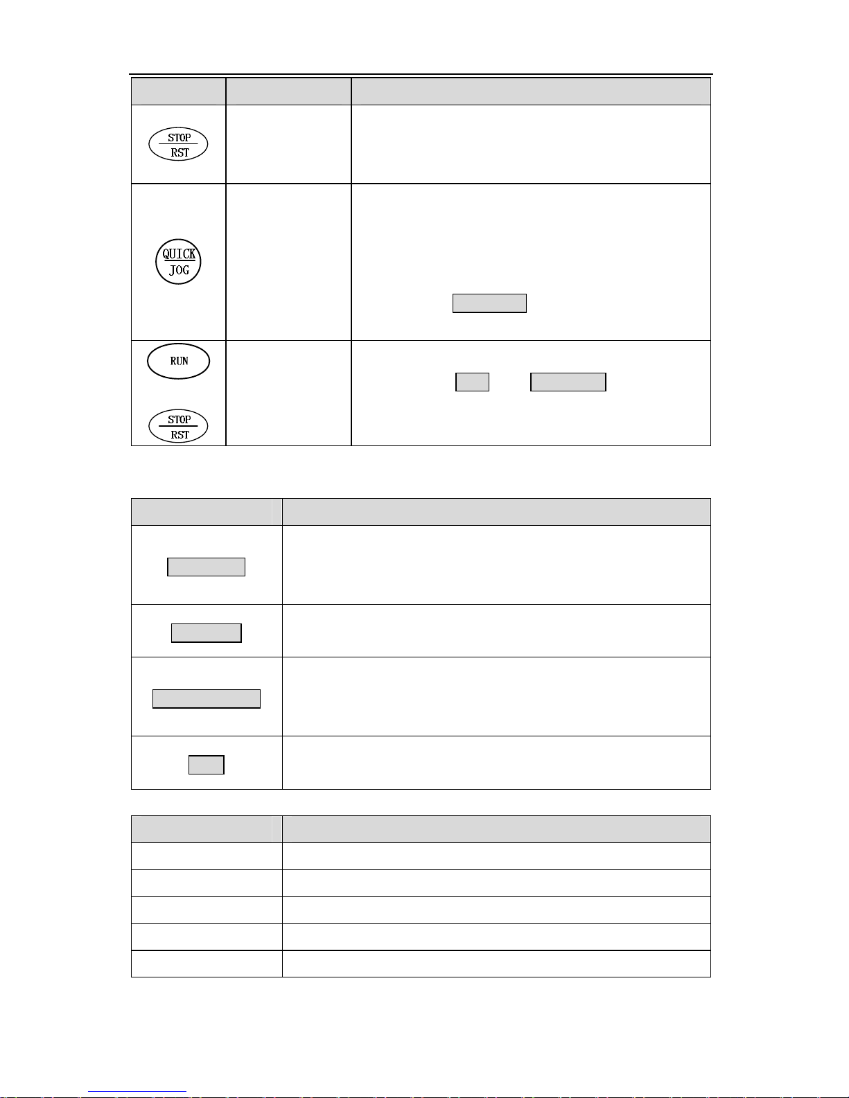
Key Name Function Description
Programming
UP Increment
Decrement Key
Right shift Key
Key
Enter Key Progressively enter menu and confirm parameters.
Key
DOWN
Run Key Start to run the inverter in keypad control mode.
Entry or escape of first-level menu.
Progressively increase data or function codes.
Progressive decrease data or function codes.
In parameter setting mode, press this button to
select the bit to be modified. In other modes,
cyclically displays parameters by right shift
.27.
CHF100A series high performance universal inverter
+
Key Name Function Description
STOP/RESET
In running status, restricted by P7.04, can be used
to stop the inverter. When fault alarm, can be used
Key
to reset the inverter without any restriction.
Determined by Function Code P7.03:
0: Display status switching
1: Jog operation
Shortcut Key
2: Switch between forward and reverse
3: Clear the UP/DOWN settings.
4: Quick debugging mode
Combination
Key
Pressing the RUN and STOP/RST at the same
time can achieve inverter coast to stop.
5.1.3 Indicator light description
5.1.3.1 Function Indicator Light Description
Function indicator
Description
Extinguished: stop status
RUN/TUNE
Flickering: parameter autotuning status
Light on: operating status
Extinguished: forward operation
FWD/REV
Light on: reverse operation.
Extinguished: keypad control
LOCAL/REMOT
Flickering: terminal control
Light on: communication control
Extinguished: normal operation status
TRIP
Flickering: overload pre-warning status
5.1.3.2 Unit Indicator Light Description
Unit indicator Description
Hz Frequency unit
A Current unit
V Voltage unit
RPM Rotating speed unit
% Percentage
5.1.3.3 Digital Display
.28.

CHF100A series high performance universal inverter
Have 5 digit LED , which can display all kinds of monitoring data and alarm codes such
as reference frequency, output frequency and so on.
5.2 Operation Process
5.2.1 Parameter setting
Three levels of menu are:
l Function code group (first-level);
l Function code (second-level);
l Function code value (third-level).
Remarks:
Press both the PRG/ESC and the DATA/ENT can return to the second-class menu from
the third-class menu. The difference is: pressing DATA/ENT will save the set parameters
into the control panel, and then return to the second-class menu with shifting to the next
function code automatically; while pressing PRG/ESC will directly return to the
second-class menu without saving the parameters, and keep staying at the current
function code.
Figure 5.2 Flow chart of parameter setting.
Under the third-class menu, if the parameter has no flickering bit, it means the function
code cannot be modified. The possible reasons could be:
l This function code is not modifiable parameter, such as actual detected parameter,
operation records and so on;
.29.

CHF100A series high performance universal inverter
l This function code is not modifiable in running status, but modifiable in stop status.
5.2.2 Fault reset
If the inverter has fault, it will prompt the related fault information. User can use
STOP/RST or according terminals determined by P5 Group to reset the fault. After fault
reset, the inverter is at stand-by state. If user does not reset the inverter when it is at fault
state, the inverter will be at operation protection state, and can not run.
5.2.3 Motor parameters autotuning
The procedure of motor parameter autotuning is as follows:
Firstly, choose the keypad command channel as the operation command channel
(P0.01).
And then input following parameters according to the actual motor parameters:
P2.01: motor rated power.
P2.02: motor rated frequency;
P2.03: motor rated speed;
P2.04: motor rated voltage;
P2.05: motor rated current;
Notice: the motor should be uncoupled with its load; otherwise, the motor parameters
obtained by autotuning may be not correct.
Set P0.16 to be 1, and for the detail process of motor parameter autotuning, please refer
to the description of Function Code P0.16. And then press RUN on the keypad panel,
the inverter will automatically calculate following parameter of the motor:
P2.06: motor stator resistance;
P2.07: motor rotor resistance;
P2.08: motor stator and rotor inductance;
P2.09: motor stator and rotor mutual inductance;
P2.10: motor current without load;
Then motor autotuning is finished.
5.2.4 Password setting
CHF100A series inverter offers user’s password protection function. When P7.00 is set
to be nonzero, it will be the user’s password, and after exiting function code edit mode, it
will become effective after 1 minute. If pressing the PRG/ESC again to try to access the
function code edit mode, “ ------” will be displayed, and the operator must input correct
user’s password, otherwise will be unable to access it.
If it is necessary to cancel the password protection function, just set P7.00 to be zero.
.30.

CHF100A series high performance universal inverter
5.2.5 Shortcut menu setting
Shortcut menu, in which parameters in common use can be programmed, provides a
quick way to view and modify function parameters. In the shortcut menu, a parameter
being displayed as “hP0.11” means the function parameter P0.11. Modifying parameters
in the shortcut menu has the same effect as doing at normal programming status.
Maximum 16 function parameters can be saved into the shortcut menu, and these
parameters can be added or deleted when P7.03 is set to be 0.
5.3 Running State
5.3.1 Power-on initialization
Firstly the system initializes during the inverter power-on, and LED displays “8.8.8.8.8.8”.
After the initialization is completed, the inverter is in stand-by status
5.3.2 Stand-by
At stop or running status, parameters of multi-status can be displayed. Whether or not to
display this parameter can be chosen through Function Code P7.06, P7.07 (Running
status display selection) and P7.08 (Stop status display selection) according to binary
bits, the detailed description of each bit please refer the function code description of
P7.06, P7.07 and P7.08.
In stop status, there are ten parameters which can be chosen to display or not. They are:
reference frequency, DC bus voltage, ON-OFF input status, open collector output status,
PID setting, PID feedback, analog input AI1 voltage, analog input AI2 voltage, HDI
frequency, step number of simple PLC and multi-step speed. Whether or not to display
can be determined by setting the corresponding binary bit of P7.08. Press the 》/SHIFT
to scroll through the parameters in right order. Press DATA/ENT + QUICK/JOG to scroll
through the parameters in left order.
5.3.3 Operation
In running status, there are nineteen running parameters which can be chosen to display
or not. They are: running frequency, reference frequency, DC bus voltage, output voltage,
output current, rotating speed, line speed, output power, output torque, PID setting, PID
feedback, ON-OFF input status, open collector output status, length value, count value,
step number of PLC and multi-step speed, voltage of AI1, voltage of AI2, high speed
pulse input HDI frequency. Whether or not to display can be determined by setting the
corresponding bit of P7.06, P7.07. Press the 》/SHIFT to scroll through the parameters
in right order. Press DATA/ENT + QUICK/JOG to scroll through the parameters in left
order.
.31.

CHF100A series high performance universal inverter
5.3.4 Fault
In fault status, inverter will display parameters of STOP status besides parameters of
fault status. Press the 》/SHIFT to scroll through the parameters in right order . Press
DATA/ENT + QUICK/JOG to to scroll through the parameters in left order.
CHF series inverter offers a variety of fault information. For details, see inverter faults
and their troubleshooting.
5.4 Shortcut Menu
Shortcut menu provides a quick way to view and modify function parameters.
Seting the P7.03 to be 4, the press QUICK/JOG, the inverter will search the parameter
which is different from the factory seting, save these parameters to be ready for checking.
The buffer length of shortcut menu is 32. So when the record data beyonds to 32, can
not display the overlength part. Press QUICK/JOGwill be the shortcut debugging mode.
If the UICK/JOG display “NULLP”, It means the parameters is the same with the factory
setting. If want to return to last display, press QUICK/JOG.
.32.

CHF100A series high performance universal inverter
6. DETAILED FUNCTION DESCRIPTION
6.1 P0 Group--Basic Function
Function
Code
P0.00
0: V/F control: It is suitable for general purpose application such as pumps, fans etc.
1: Sensorless vector control: It is widely used for the application which requires high
torque at low speed, high speed accuracy, and quicker dynamic response, such as
machine tool, injection molding machine, centrifugal machine and wire-drawing machine,
etc.
2. Torque control: It is suitable for the application with low accuracy torque control, such
as wired-drawing.
Notice:
l The autotuning of motor parameters must be accomplished properly If you
Name Description
0: V/F control
Control
1: Sensorless vector control
model
2: Torque control
Setting
Range
0~2 0
Factory
Setting
use the sensorless vector control mode or Torque control mode. How to
autotuning of motor parameters please refer to page 36
l In order to achieve better control characteristic, the parameters of vector
control (P3 Group) should be adjusted.
Function
Code
P0.01
The control commands of inverter include: start, stop, forward run, reverse run, jog, fault
reset and so on.
0: Keypad (LED extinguished);
Both RUN and STOP/RST key are used for running command control. If Multifunction
key QUICK/JOG is set as FWD/REV switching function (P7.03 is set to be 1), it will be
used to change the rotating orientation. In running status, pressing RUN and
STOP/RST in the same time will cause the inverter coast to stop.
Name Description
0: Keypad (LED extinguished)
Run
1: Terminal (LED flickering)
command
2: Communication (LED lights
source
on)
Setting
Range
0~2 0
Factory
Setting
.33.

CHF100A series high performance universal inverter
1: Terminal (LED flickering)
The operation, including forward run, reverse run, forward jog, reverse jog etc. can be
controlled by multifunctional input terminals.
2: Communication (LED lights on)
The operation of inverter can be controlled by host through communication.
Function
Setting
Factory
Name Description
Code
Range
Setting
0: Valid, save UP/DOWN value
when power off
1: Valid, do not save
P0.02
UP/DOWN
setting
UP/DOWN value when power
0~3 0
off
2: Invalid
3: Valid during running, clear
when stop.
0: User can adjust the reference frequency by UP/DOWN. The value of UP/DOWN can
be saved when power off.
1: User can adjust the reference frequency by UP/DOWN, but the value of UP/DOWN
will not be saved when power off.
2: User can not adjust the reference frequency by UP/DOWN. The value of UP/DOWN
will be cleared.
3: User can only adjust the reference frequency by UP/DOWN during the inverter is
running. The value of UP/DOWN will be cleared when the inverter stops.
Notice:
l UP/DOWN function can be achieved by keypad (∧ and ∨) and
multifunctional terminals.
l Reference frequency can be adjusted by UP/DOWN.
l UP/DOWN has highest priority which means UP/DOWN is always active no
matter which frequency command source is.
l When the factory setting is restored (P0.17 is set to be 1), the value of
UP/DOWN will be cleared.
Function
Setting
Factory
Name Description
Code
Range
Setting
Maximum
P0.03
10.00~400.00Hz 10.00~400.00 50.00Hz
frequency
.34.

CHF100A series high performance universal inverter
Notice: The frequency reference should not exceed maximum frequency, and it is
the basis of ramping time of ACC/DEC.
Function
Setting
Factory
Name Description
Code
Range
Setting
Upper
P0.04
P0.05~P0.03 P0.05~P0.03
50.00Hz
frequency limit
Notice:
l Upper frequency limit should exceed than the maximum frequency
l Output frequency should not exceed upper frequency limit.
Function
Setting
Factory
Name Description
Code
Range
Setting
Lower
P0.05
frequency
0.00~P0.04 0.00~P0.04
0.00Hz
limit
Notice:
l Lower frequency limit should exceed than upper frequency limit (P0.04).
l If frequency reference is lower than P0.05, the action of inverter is
determined by P1.12. Please refer to description of P1.12.
Function
Setting
Factory
Name Description
Code
Range
Setting
Keypad
P0.06
reference
0.00~P0.03 0.00~P0.03 50.00Hz
frequency
When Frequency A command source is set to be Keypad, this parameter is the initial
value of inverter reference frequency.
Function
Setting
Factory
Name Description
Code
Range
Setting
0: Keypad
1: AI1
2. AI2
Frequency
3: HDI
P0.07
A command
0~7 0
4. Simple PLC
source
5: Multi-step speed
6: PID
7: Communication
.35.

CHF100A series high performance universal inverter
0: Keypad: Please refer to description of P0.06
1: AI1
2: AI2
The reference frequency is set by analog input. AI1 is -10V~10V voltage input terminal,
while AI2 is 0~10V/0(4)~20mA, which can be selected by J16. When AI2 is selected to
be 0~20mA, which corresponds with 5V.
3: HDI
The reference frequency is set by high speed pulse input.
Pulse specification: pulse voltage range 15~30V, and pulse frequency range 0.0~50.0
kHz. 100% of the setting inpluse corresponds with maximal frequency, while -100%
corresponds with minus maximal frequency.
4. Simple PLC
User can set reference frequency, hold time, running direction of each step and
acceleration/deceleration time between steps. For details, please refer to description of
PA group.
5. Multi-step speed
The reference frequency is determined by P5 and PA group. The selection of steps is
determined by combination of multi-step speed terminals.
Notice:
l Multi-step speed mode will enjoy priority in setting reference frequency if
P0.03 is not set to be 4 or 5. In this case, only step 1 to step 15 are available.
l If P0.03 is set to be 5, step 0 to step 15 can be realized.
l Jog has highest priority.
6. PID
The reference frequency is the result of PID adjustment. For details, please refer to
description of P9 group.
7. Communication
The reference frequency is set through RS485. For details, please refer to Modbus
protocol in Chapter 9.
Function
Setting
Factory
Name Description
Code
Range
Setting
Frequency
P0.08
B command
source
0:AI1
1:AI2
2:HDI
0~2 0
.36.

CHF100A series high performance universal inverter
For details, please refer to P0.07.
Function
Setting
Factory
Name Description
Code
Range
Setting
Scale of
0: Maximum frequency
P0.09
frequency B
0~1 0
1: Frequency A command
command
Notice: If set AI2 to be 0~20mA input, the relative voltage of 20mA is 5V. P0.09 is
used when the frequeny B is superimposed.
Function
Setting
Factory
Name Description
Code
Range
Setting
0: A
Frequency
1: B
P0.10
command
0~3 0
2: A+B
selection
3: Max(A, B)
This parameter can be used to select the reference frequency command.
0: Only frequency command source A is active.
1: Only Frequency command source B is active.
2: Both Frequency command source A and B are active.
Reference frequency = reference frequency A + reference frequency B.
3: Both Frequency command source A and B are active.
Reference frequency = Max (reference frequency A, reference frequency B).
Notice: Combination (0、1、2)can be switched by Multifunctional terminal S1~S7
Function
Setting
Factory
Name Description
Code
P0.11
P0.12
Acceleration
0.1~3600.0s 0.1~3600.0
time 0
Deceleration
0.1~3600.0s 0.1~3600.0
time 0
Range
Setting
Depend
on model
Depend
on model
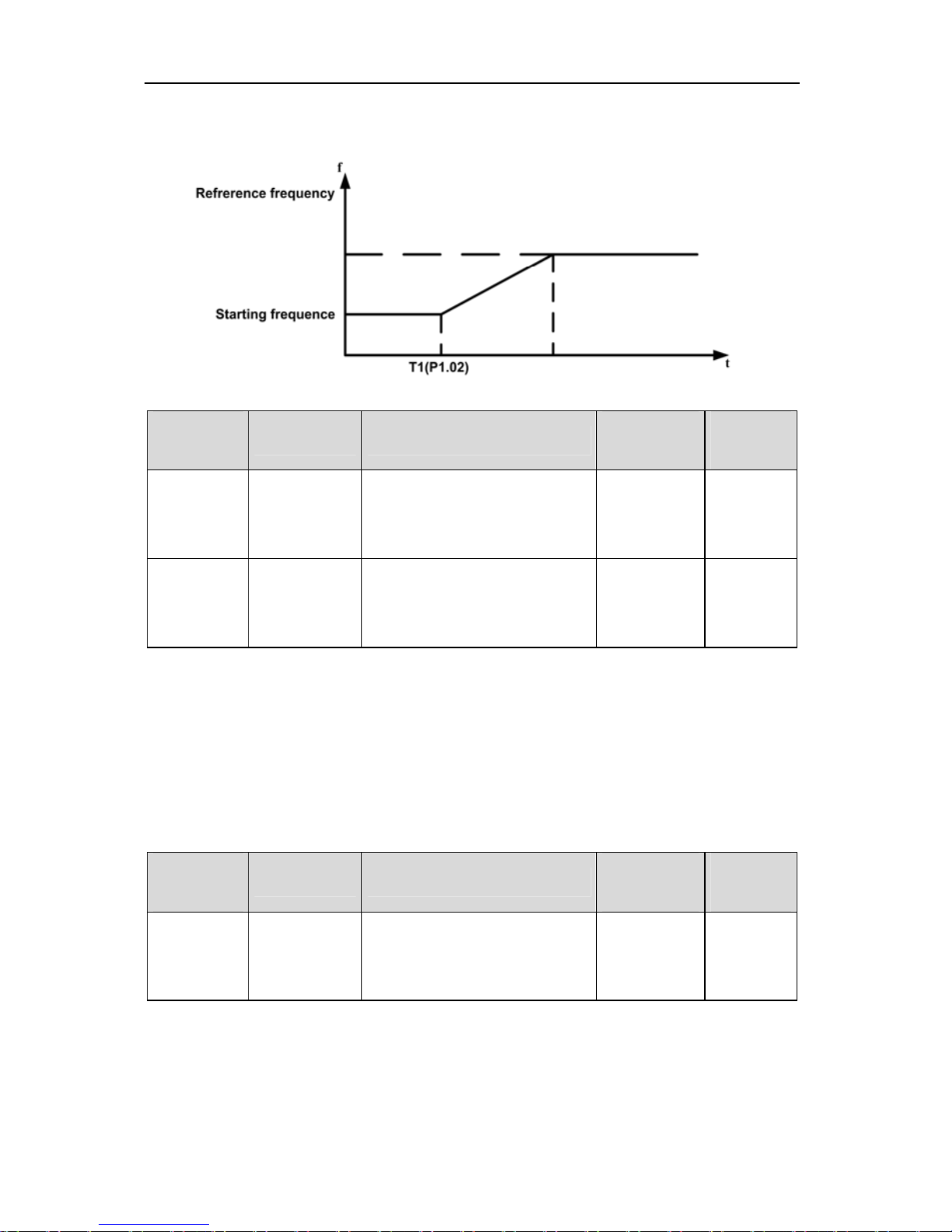
Acceleration time is the time of accelerating from 0Hz to maximum frequency (P0.03).
Deceleration time is the time of decelerating from maximum frequency (P0.03) to 0Hz.
Please refer to following figure.
.37.

CHF100A series high performance universal inverter
Figure 6.1 Acceleration and deceleration time.
When the reference frequency is equal to the maximum frequency, the actual
acceleration and deceleration time will be equal to actual setting.
When the reference frequency is less than the maximum frequency, the actual
acceleration and deceleration time will be less than actual setting.
The actual acceleration (deceleration) time = setting ACC/DEC time* referrence
frequency/ maximum frequency.
1st group: P0.11, P0.12
2nd group: P8.00, P8.01
3rd group: P8.02, P8.03
4th group: P8.04, P8.05.
The acceleration and deceleration time can be selected by combination of
multifunctional ON-OFF input terminals.
Function
Code
P0.13
Notice: If the parameters are restored, the running direction will be back to its
original status.
Function
Code
Name Description
Running
direction
selection
Name Description
0: Forward
1: Reverse
2: Forbid reverse
Setting
Range
0~2 0
Setting
Range
Factory
Factory
Setting
Setting
P0.14
Carrier
frequency
1.0~15.0kHz 1.0~15.0
Depend
on model
.38.
CHF100A series high performance universal inverter
Figure 6.2 Effect of carrier frequency.
The following table is the relationship between power rating and carrier frequency.
Carrier f
Model
0.4kW~11kW 15 1.0 8
15kW~55kW 8 1.0 4
75kW~630kW 6 1.0 2
Carrier frequency will affect the noise of motor and the EMI of inverter.
If the carrier frequency is increased, it will cause better current wave, less harmonic
current and lower noise of motor.
Notice:
l The factory setting is optimal in most cases. Modification of this parameter
is not recommended.
l If the carrier frequency exceeds the factory setting, the inverter must be
derated because the higher carrier frequency will cause more switching loss,
higher temperature rise of inverter and stronger electromagnetic interference.
l If the carrier frequency is lower than the factory setting, it is possible to
cause less output torque of motor and more harmonic current.
Highest Carrier f
( kHz )
Lowest Carrier f
( kHz )
Factory setting
( kHz )
Function
Code
P0.15
Notice: AVR function is automatical debugging of output voltage
Name Description
AVR
function
Setting
Range
0~2 0~2 1
.39.
Factory
Setting

CHF100A series high performance universal inverter
Function
Setting
Factory
Name Description
Code
P0.16
Motor
parameters
autotuning
0: No action
1: Rotation autotuning
2: Static autotuning
Range
Setting
0~2 0
0: No action: Forbidding autotuning.
1: Rotation autotuning:
u Do not connect any load to the motor when performing autotuning and ensure the
motor is in static status.
u Input the nameplate parameters of motor (P2.01- P2.05) correctly before
performing autotuning. Otherwise the parameters detected by autotuning will be
incorrect; it may influence the performance of inverter.
u Set the proper acceleration and deceleration time (P0.11 and P0.12) according to
the motor inertia before performing autotuning. Otherwise it may cause
over-current and over-voltage fault during autotuning.
u The operation process is as follow:
a. Set P0.16 to be 1 then press the DATA/ENT, LED will display “-TUN-” and
flickers. During “-TUN-” is flickering, press the PRG/ESC to exit autotuning.
b. Press the RUN to start the autotuning, LED will display “TUN-0”.
c. After a few seconds the motor will start to run. LED will display “TUN-1” and
“RUN/TUNE” light will flicker.
d. After a few minutes, LED will display “-END-”. That means the autotuning is
finished and return to the stop status.
e. During the autotuning, press the STOP/RST will stop the autotuning.
Notice: Only keypad can control the autotuning. P0.12 will restore to 0
automatically when the autotuning is finished or cancelled.
2: Static autotuning:
u If it is difficult to disconnect the load, static autotuning is recommended.
u The operation process is the same as rotation autotuning except step c.
Notice: The Mutual inductance and current without load will not be detected by
static autotuning, if needed user should input suitable value according to
experience.
.40.

CHF100A series high performance universal inverter
Function
Code
P0.17
0: No action
1: Inverter restores all parameters to factory setting except P2 group.
2: Inverter clear all fault records.
This function code will restore to 0 automatically when complete the function operation.
Name Description
0: No action
Restore
1: Restore factory setting
parameters
2: Clear fault records
Setting
Range
0~2 0
Factory
Setting
6.2 P1 Group --Start and Stop Control
Function
Name Description
Code
P1.00 Start Mode
0: Start directly
1: DC braking and start
2: Speed tracking and start
Setting
Range
0~2 0
Factory
Setting
0: Start directly: Start the motor at the starting frequency determined by P1.01.
1: DC braking and start: Inverter will output DC current firstly and then start the motor at
the starting frequency. Please refer to description of P1.03 and P1.04. It is suitable for
the motor which have small inertia load and may reverse rotation when start.
2: Speed tracking and start: Inverter detects the rotation speed and direction of motor,
then start running to its reference frequency based on current speed. This can realize
smooth start of rotating motor with big inertia load when instantaneous power off.
Notice: It only applies on the inverter of 7.5kW and above.
Function
Code
P1.01
P1.02
Notice:
Name Description
Starting
frequency
Hold time of
starting
frequency
0.00~10.00Hz 0.00~10.00
0.0~50.0s 0.0~50.0 0.0s
Setting
Range
Factory
Setting
0.00Hz
l Set proper starting frequency can increase the starting torque.
l If the reference frequency is less than starting frequency, inverter will be at
stand-by status. The indicator of RUN/TUNE lights on, inverter has no output.
.41.
CHF100A series high performance universal inverter
l The starting frequency could be less than the lower frequency limit (P0.05).
l P1.01 and P1.02 take no effect during FWD/REV switching.
Figure 6.3 Starting diagram.
Function
Code
P1.03
P1.04
When inverter starts, it performs DC braking according to P1.03 firstly, then start to
accelerate after P1.04.
Notice:
l DC braking will take effect only when P1.00 is set to be 1.
l DC braking is invalid when P1.04 is set to be 0.
l The value of P1.03 is the percentage of rated current of inverter. The bigger
the DC braking current, the greater the braking torque.
Function
Code
Name Description
DC Braking
current
before start
DC Braking
time before
start
Name Description
0.0~150.0% 0.0~150.0
0.0~50.0s 0.0~50.0 0.0s
Setting
Range
Setting
Range
Factory
Setting
0.0%
Factory
Setting
Acceleration /
P1.05
0: Linear: Output frequency will increase or decrease with fixed acceleration or
deceleration time.
1: Reserved
Notice: CHF100A inverter offers 4 groups of specific acceleration and deceleration
Deceleration
mode
0: Linear
0~1 0
1: reserved
.42.

CHF100A series high performance universal inverter
time, which can be determined by the multifunctional ON-OFF input terminals (P5
Group).
Function
Setting
Factory
Name Description
Code
Range
Setting
0: Deceleration to stop
P1.06 Stop mode
0~1 0
1: Coast to stop
0: Deceleration to stop
When the stop command takes effect, the inverter decreases the output frequency
according to P1.05 and the defined deceleration time till stop.
1: Coast to stop
When the stop command takes effect, the inverter blocks the output immediately. The
motor coasts to stop by its mechanical inertia.
Function
Setting
Factory
Name Description
Code
Range
Setting
Starting
P1.07
frequency of
0.00~P0.03 0.00~P0.03
0.00Hz
DC braking
Waiting time
P1.08
before DC
0.0~50.0s 0.0~50.0 0.0s
braking
DC braking
P1.09
0.0~150.0% 0.0~150.0
0.0%
current
DC braking
P1.10
0.0~50.0s 0.0~50.0 0.0s
time
Starting frequency of DC braking: Start the DC braking when running frequency reaches
starting frequency determined by P1.07.
Waiting time before DC braking: Inverter blocks the output before starting the DC braking.
After this waiting time, the DC braking will be started so as to prevent over-current fault
caused by DC braking at high speed.
DC braking current: The value of P1.09 is the percentage of rated current of inverter. The
bigger the DC braking current is, the greater the braking torque is.
DC braking time: The time used to perform DC braking. If the time is 0, the DC braking
will be invalid.
.43.

CHF100A series high performance universal inverter
0: Running at the lower
Figure 6.4 DC braking diagram.
Function
Code
P1.11
Set the hold time at zero frequency in the transition between forward and reverse
running.
It is shown as following figure:
Name Description
Dead time of
0.0~3600.0s 0.0~3600.0
FWD/REV
Setting
Range
Factory
Setting
0.0s
Function
Code
P1.12
Name Description
Action when
running
frequency is
less than
lower
frequency limit
Figure 6.5 FWD/REV dead time diagram.
frequency limit
1: Stop
2: Stand-by
.44.
Setting
Range
0~2 0
Factory
Setting

CHF100A series high performance universal inverter
when power is
0: Running at the lower frequency limit (P0.05): The inverter runs at P0.05 when the
running frequency is less than P0.05.
1: Stop: This parameter is used to prevent motor running at low speed for a long time.
2: Stand-by: Inverter will Coast to stop when the running frequency is less than P0.05.
When the reference frequency is higher than or equal to P0.05 again, the inverter will
start to run automatically.
Function
Setting
Factory
Name Description
Code
Range
Setting
Delay time
P1.13
0.0~3600.0s 0.0~3600.0
0.0s
for restart
P1.14
Restart after
power off
0: Disabled
0~1 0
1: Enabled
0: Disabled: Inverter will not automatically restart when power on again until run
command takes effect.
1: Enabled: When inverter is running, after power off and power on again, if run
command source is key control (P0.01=0) or communication control (P0.01=2), inverter
will automatically restart after delay time determined by P1.14; if run command source is
terminal control (P0.01=1), inverter will automatically restart after delay time determined
by P1.14 only if FWD or REV is active.
Notice:
l If P1.14 is set to be 1, it is recommended that start mode should be set as
speed tracing mode (P1.00=2).
l This function may cause the inverter restart automatically, please be
cautious.
Function
Setting
Factory
Name Description
Code
Range
Setting
Waiting time
P1.15
0.0~3600.0s 0.0~3600.0s
0.0
of restart
Notice: Valid when P1.14=1
Function
Setting
Factory
Name Description
Code
Range
Setting
Terminal
P1.16
function
examined
0: Disabled
0~1 0
1: Enabled
.45.

CHF100A series high performance universal inverter
on
Notice:
l This function only takes effect if run command source is terminal control.
l If P1.15 is set to be 0, when power on, inverter will not start even if FWD/REV
terminal is active, until FWD/REV terminal disabled and enabled again.
l If P1.15 is set to be 1, when power on and FWD/REV terminal is active,
inverter will start automatically.
l This function may cause the inverter restart automatically, please be
cautious.
Function
Name Description
Code
P1.17~P1.19
Reversed
6.3 P2 Group--Motor Parameters
Function
Code
P2.00
0: G model: Applicable to constant torque load.
1: P model: Applicalbe to constant power load.
Function
Code
P2.01
Name Description
Inverter
model
0: G model
1: P model
Name Description
Motor rated
0.4~3000.0kW 0.4~3000.0
power
Setting
Factory
Range
Setting
Factory
Range
0~1 0
Setting
Factory
Range
on model
Setting
Setting
Setting
Depend
P2.02
Motor rated
frequency
Motor rated
P2.03
speed
Motor rated
P2.04
voltage
Motor rated
P2.05
current
Notice:
l In order to achieve superior performance, please set these parameters
10Hz~P0.03 10~P0.03
0~36000rpm 0~36000
0~800V 0~800V
0.8~6000.0A 0.8~6000.0
.46.
50.00Hz
Depend
on model
Depend
on model
Depend
on model

CHF100A series high performance universal inverter
ASR switching
according to motor nameplate, and then perform autotuning.
l The power rating of inverter should match the motor. If the bias is too big,
the control performances of inverter will be deteriorated distinctly.
l Reset P2.01 can initialize P2.06~P2.10 automatically.
Function
Code
P2.06
P2.07
P2.08
P2.09
P2.10
After autotuning, the value of P2.06~P2.09 will be automatically updated.
Notice: Do not change these parameters, otherwise it may deteriorate the control
performance of inverter.
Name Description
Motor stator
resistance
Motor rotor
resistance
Motor
leakage
inductance
Motor mutual
inductance
Current
without load
0.001~65.535Ω 0.001~65.535
0.001~65.535Ω 0.001~65.535
0.1~6553.5mH 0.1~6553.5
0.1~6553.5mH 0.1~6553.5
0.01~655.35A 0.01~655.35
Setting
Range
Factory
Setting
Depend
on model
Depend
on model
Depend
on model l
Depend
on model
Depend
on model
6.4 P3 Group—Vector Control
Function
Code
P3.00
P3.01
P3.02
P3.03
Name Description
ASR
proportional
gain Kp1
ASR integral
time Ki1
point 1
ASR
proportional
gain Kp2
0~100 0~100 20
0.01~10.00s 0.01~10.00
0.00Hz~P3.05 0.00~P3.05
0~100 0~100 25
.47.
Setting
Range
Factory
Setting
0.50s
5.00Hz

CHF100A series high performance universal inverter
ASR switching
Function
Setting
Factory
Name Description
Code
Range
Setting
ASR integral
P3.04
0.01~10.00s 0.01~10.00
1.00s
time Ki2
P3.05
P3.02~P0.03 P3.02~P0.03 10.00Hz
point 2
P3.00~P3.05 are only valid for vector control and torque control and invalid for V/F
control. Through P3.00~P3.05, user can set the proportional gain Kp and integral time Ki
of speed regulator (ASR), so as to change the speed response characteristic. ASR's
structure is shown in following figure.
Figure 6.6 ASR diagram.
P3.00 and P3.01 only take effect when output frequency is less than P3.02. P3.03 and
P3.04 only take effect when output frequency is greater than P3.05. When output
frequency is between P3.02 and P3.05, Kp and KI are proportional to the bias between
P3.02 and P3.05. For details, please refer to following figure.
Figure 6.7 PI parameter diagram.
The system's dynamic response can be faster if the proportion gain Kp is increased;
However, if Kp is too large, the system tends to oscillate.
The system dynamic response can be faster if the integral time Ki is decreased;
However, if Ki is too small, the system becomes overshoot and tends to oscillate.
P3.00 and P3.01 are corresponding to Kp and Ki at low frequency, while P3.03 and P3.04
are corresponding to Kp and Ki at high frequency. Please adjust these parameters
according to actual situation. The adjustment procedure is as follow:
.48.

CHF100A series high performance universal inverter
u Increase the proportional gain (Kp) as far as possible without creating oscillation.
u Reduce the integral time (Ki) as far as possible without creating oscillation.
For more details about fine adjustment, please refer to description of P9 group.
Function
Setting
Factory
Name Description
Code
Range
Setting
Slip
P3.06
compensation
50.0%~200.0% 50~200 100%
rate of VC
The parameter is used to adjust the slip frequency of vector control and improve the
precision of speed control. Properly adjust this parameter can effectively restrain the
static speed bias.
Function
Setting
Factory
Name Description
Code
P3.07
Torque upper
0.0~200.0% 0~200
limit
Range
Setting
Depend
on model
Notice:
l 100% setting corresponding to rated current. G model : 150.0%;P model:
120.0%.
l Under torque control, P3.07 and P3.09 are all related with torque setting.
Function
Setting
Factory
Name Description
Code
Range
Setting
0: Keypad (P3.09)
1:AI1
Torque
2:AI2
P3.08
setting
0~5 0
3:HDI
source
4:Multi-step speed
5:Communication
0: Keypad (P3.09)
1:AI1
2:AI2
3:HDI
4:Multi-step speed
5:Communication
1~5: Torque control is valid, which defines the torque setting source. When the torque
setting is minus, the motor will reverse.
.49.

CHF100A series high performance universal inverter
Under speed control model, output torque matches load torque automatically, but limited
by P3.07.
Under torque control model, output torque is limited by upper and lower frequency limit.
Notice:
l speed control and torque control can be switched by using multi-function
input terminals.
l 1~5:100% corresponding to twice of rated current of inverter.
l When inverter decelerate to stop, Torque control model is switched to speed
control mode automatically
Function
Name Description Setting Range
Code
Keypad
P3.09
torque
-200.0%~200.0% -200.0%~200.0% 50.0%
setting
0: Keypad (P0.04)
Upper
frequency
1: AI1
2: AI2
P3.10
setting
source
3: HDI
4: Multi-step
5: Communication
Notice: 1~4 100% Corresponding to maximum frequency.
6.5 P4 Group—V/F Control
Function
Code
Name Description
Factory
Setting
0~5 0
Setting
Range
Factory
Setting
P4.00
V/F curve
selection
0: Linear V/F curve. It is applicable for normal constant torque load.
1: User-defined curve. It can be defined through setting (P4.03~P4.08).
0:Linear V/F curve
1: User-defined curve
2: Torque_stepdown curve
(1.3 order)
0~4 0
3: Torque_stepdown curve
(1.7 order)
4: Torque_stepdown curve
(2.0 order)
.50.

CHF100A series high performance universal inverter
2~4: Torque_stepdown curve. It is applicable for variable torque load, such as blower,
pump and so on. Please refer to following figure.
Notice:Vb= Motor rated voltage Fb= Motor rated frequency.
Figure 6.8 V/F curve.
Function
Code
P4.01 Torque boost
P4.02
Torque boost will take effect when output frequency is less than cut-off frequency of
torque boost (P4.02). Torque boost can improve the torque performance of V/F control at
low speed.
The value of torque boost should be determined by the load. The heavier the load, the
larger the value.
Notice: This value should not be too large, otherwise the motor would be
over-heat or the inverter would be tripped by over-current or over-load.
If P4.01 is set to be 0, the inverter will boost the output torque according to the load
automatically. Please refer to following diagram.
Name Description
0.0%: (auto)
0.1%~10.0%
Torque boost
cut-off
0.0%~50.0% (motor rated
frequency)
Setting
Range
0.0~10.0 0.0%
0.0~50.0 20.0%
Factory
Setting
.51.

CHF100A series high performance universal inverter
Figure 6.9 Torque boost by hand.
Function
Factory
Name Description Setting Range
Code
Setting
V/F
P4.03
0.00Hz~P4.05 0.00~P4.05 0.00Hz
frequency 1
P4.04 V/F voltage 1 0.0%~100.0% 0.0~100.0 0.0%
V/F
P4.05
P4.03~P4.07 P4.03~ P4.07
0.00Hz
frequency 2
P4.06 V/F voltage 2 0.0%~100.0% 0.0~100.0 0.0%
V/F
P4.07
P4.05~P2.02 P4.05~ P2.02
0.00Hz
frequency 3
P4.08 V/F voltage 3 0.0%~100.0% 0.0~100.0 0.0%
This function is only active when P4.00 is set to be 1. P4.03~P4.08 are used to set the
user-defined V/F curve. The value should be set according to the load characteristic of
motor.
Notice:
l 0<V1<V2<V3<rated voltage.
l 0<f1<f2<f3<rated frequency.
l The voltage corresponding to low frequency should not be set too high,
otherwise it may cause motor overheat or inverter fault.
Figure 6.10 V/F curve setting diagram.
.52.

CHF100A series high performance universal inverter
Function
Setting
Factory
Name Description
Code
Range
Setting
Slip
P4.09
compensation
0.00~200.0% 0.00~200.00
0.0%
limit
The slip compensation function calculates the torque of motor according to the output
current and compensates for output frequency. This function is used to improve speed
accuracy when operating with a load. P4.09 sets the slip compensation limit as a
percentage of motor rated slip, the slip compensation limit is calculated as the formula:
P4.09=fb-n*p/60
Fb= Motor rated frequency (P2.02)
N= Motor rated speed (P2.03)
P= Motor poles
Function
Setting
Factory
Name Description
Code
Range
Setting
Auto energy
0: Disabled
P4.10
saving
0~1 0
1: Enabled
selection
When P4.10 is set to be 1, while there is a light load such as pumps or fans, it will reduce
the inverter output voltage and save energy.
Function
Setting
Factory
Name Description
Code
Range
Setting
Low-frequency
threshold of
P4.11
0~10 0~10
2
restraining
oscillation
High-frequency
threshold of
P4.12
0~10 0~10
0
restraining
oscillation
Boundary of
P4.13
restraining
0.0~P3.03 0.0~P3.03
30Hz
oscillation
P4.11~P4.12 are only valid in the V/F control mode, When set P4.11 and P4.12 to be 0, the
restraining oscillation is invalid. While set the values to be 1~3 will have the effect of
.53.

CHF100A series high performance universal inverter
restraining oscillation.When the running frequency is lower than P4.13, P4.11 is valid,
when the running frequency higher than P4.13, P4.12 is valid.
6.6 P5 Group--Input Terminals
Function
Name Description
Code
P5.00 HDI selection
S1 terminal
P5.01
function
S2 terminal
P5.02
function
S3 terminal
P5.03
function
S4 terminal
P5.04
function
S5 terminal
P5.05
function
P5.06 S6 terminal
function
0: High speed pulse input
1: ON-OFF input
Programmable multifunctional
terminal
Programmable multifunctional
terminal
Programmable multifunctional
terminal
Programmable multifunctional
terminal
Programmable multifunctional
terminal
Programmable multifunctional
terminal
Setting
Range
Factory
Setting
0~1 0
0~39 1
0~39 4
0~39 7
0~39 0
0~39 0
0~39 0
P5.07 S7 terminal
Programmable multifunctional
0~39 0
function
P5.08 HDI terminal
terminal
Programmable multifunctional
0-39 0
function
terminal
Notice: P5.08 is only used when P5.00 is set to be 1.
The meaning of each setting is shown in following table.
Setting
Function Description
value
Please set unused terminals to be invalid to avoid
0 Invalid
malfunction
1 Forward
Please refer to description of P5.10.
2 Reverse
3 3-wire control Please refer to description of P5.10.
4 Jog forward
Please refer to description of P8.06~P8.08.
5 Jog reverse
6 Coast to stop The inverter blocks the output immediately. The motor
.54.

CHF100A series high performance universal inverter
step speed
Setting
Function Description
value
7 Reset fault
8 Pause running
External fault
9
input
10 Up command
DOWN
11
command
coasts to stop by its mechanical inertia.
Resets faults that have occurred. It has the same function
as STOP/RST.
When this terminal takes effect, inverter decelerates to
stop and save current status, such as PLC, traverse
frequency and PID. When this terminal takes no effect,
inverter restores the status
Stop the inverter and output an alarm when a fault occurs
in a peripheral device.
The reference frequency of inverter can be adjusted by UP
command and DOWN command.
12
Clear
UP/DOWN
Switch between
13
A and B
Switch between
14
A and A+B
Switch between
15
B and A+B
Multi-step speed
16
reference1
Multi-
17
reference 2
Multi-step speed
18
reference 3
19 Multi-step speed
Use this terminal to clear UP/DOWN setting. Please refer
to description of P0.02.
P3.04
A B A+B
Terminal action
13 valid B A
14 valid A+B A
15 valid A+B B
16 steps speed control can be realized by the combination
of these four terminals. For details, please refer to:
Multi-step speed reference terminal status and according
step value table:
.55.

CHF100A series high performance universal inverter
ACC/DEC time 0
ACC/DEC time 1
Setting
value
20
21
22
Function Description
reference 4
Multi-step speed
pause
Keep current step unchanged no matter what the input
status of four multi-step speed terminals is.
4 groups of ACC/DEC time can be selected by the
combination of these two terminals.
ACC/DEC time
selection1
ACC/DEC time
selection 2
ACC/DEC time
selection 1
OFF OFF
OFF ON
ACC/DEC time
selection 2
ON OFF
ACC/DEC time
(P0.11、P0.12)
(P8.00、P8.01)
ACC/DEC time 2
(P8.02、P8.03)
23
Reset simple
PLC when stop
Pause simple
24
PLC
25 Pause PID
Pause traverse
26
operation
Reset traverse
27
operation
ON ON
ACC/DEC time 3
(P8.04、P8.05)
When simple PLC stops, the status of PLC such as
running step, running time and running frequency will be
cleared when this terminal is enabled.
Inverter runs at zero frequency and PLC pauses the timing
when this terminal is enabled. If this terminal is disabled,
inverter will start and continue the PLC operation from the
status before pause.
PID adjustment will be paused and inverter keeps output
frequency unchanged.
Inverter keeps output frequency unchanged. If this
terminal is disabled, inverter will continue traverse
operation with current frequency.
Reference frequency of inverter will be forced as center
frequency of traverse operation.
28 Reset counter Clear the value of counter.
29 Forbid torque Torque control is forbided and switch inverter to run in
.56.
CHF100A series high performance universal inverter
Setting
Function Description
value
control mode speed control mode.
30
Forbid the
function of
ACC/DEC is invalid and maintains output frequency if it is
enabled.
ACC/DEC
The pulse input terminal of internal counter. Maximum
31 Counter input
pulse frequency: 200Hz.
32
33~39
UP/DOWN
invalid
temporarily
Reserved Reserved
UP/DOWN setting is invalid but will not be cleared. When
this terminal is disabled, UP/DOWN value before will be
valid again.
Multi-step speed reference terminal status and according step value table:
Multi-step
Multi-step
Multi-step
Terminal
speed
speed
speed
Step
reference1
reference2
reference3
Multi-step
speed
reference4
0 OFF OFF OFF OFF
1 ON OFF OFF OFF
2 OFF ON OFF OFF
3 ON ON OFF OFF
4 OFF OFF ON OFF
5 ON OFF ON OFF
6 OFF ON ON OFF
7 ON ON ON OFF
8 OFF OFF OFF ON
9 ON OFF OFF ON
10 OFF ON OFF ON
11 ON ON OFF ON
12 OFF OFF ON ON
13 ON OFF ON ON
14 OFF ON ON ON
15 ON ON ON ON
.57.
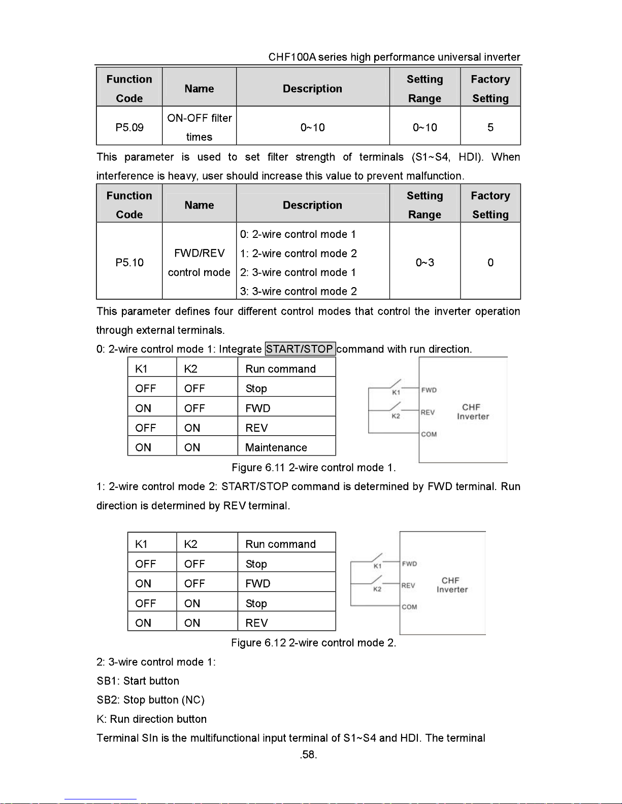


CHF100A series high performance universal inverter
Function
Code
P5.13
P5.14 AI1 upper limit -10.00V~10.00V -10.00~10.00 10.00V
P5.15
P5.16
These parameters determine the relationship between analog input voltage and the
corresponding setting value. When the analog input voltage exceeds the range between
lower limit and upper limit, it will be regarded as the upper limit or lower limit.
The analog input AI1 can only provide voltage input, and the range is -10V~10V.
Name Description
AI1 lower limit
corresponding
setting
AI1 upper limit
corresponding
setting
AI1 filter time
constant
-100.0%~100.0% -100.0~100.0
-100.0%~100.0% -100.0~100.0 100.0%
0.00s~10.00s 0.00~10.00
Setting
Range
Factory
Setting
0.0%
0.10s
For different applications, the corresponding value of 100.0% analog setting is different.
For details, please refer to description of each application.
Notice: AI1 lower limit must be less or equal to AI1 upper limit.
Figure 6.15 Relationship between AI and corresponding setting.
AI1 filter time constant is effective when there are sudden changes or noise in the analog
input signal. Responsiveness decreases as the setting increases.
Function
Name Description
Code
P5.17 AI2 lower limit
0.00V~10.00V 0.00~10.00
Setting
Range
Factory
Setting
0.00V
AI2 lower limit
P5.18
corresponding
setting
-100.0%~100.0% -100.0~100.0
.60.
0.0%

CHF100A series high performance universal inverter
.61.
Function
Code
Name Description
Setting
Range
Factory
Setting
P5.19 AI2 upper limit
0.00V~10.00V 0.00~10.00
10.00V
P5.20
AI2 upper limit
corresponding
setting
-100.0%~100.0% -100.0~100.0 100.0%
P5.21
AI2 filter time
constant
0.00s~10.00s 0.00~10.00
0.10s
Please refer to description of AI1. When AI2 is set as 0~20mA current input, the
corresponding voltage range is 0~5V.
Function
Code
Name Description
Setting
Range
Factory
Setting
P5.22
HDI lower
limit
0.0 kHz ~50.0kHz 0.0~50.0 0.0kHz
P5.23
HDI lower
limit
corresponding
setting
-100.0%~100.0% -100.0~100.0
0.0%
P5.24
HDI upper
limit
0.0 kHz ~50.0kHz 0.0~50.0 50.0kHz
P5.25
HDI upper
limit
corresponding
setting
-100.0%~100.0% -100.0~100.0 100.0%
P5.26
HDI filter time
constant
0.00s~10.00s 0.00~10.00
0.10s
The description of P5.22~P5.26 is similar to AI1.
6.7 P6 Group--Output Terminals
Function
Code
Name Description
Setting
Range
Factory
Setting
P6.00
HDO
selection
ON-OFF output 1 1
ON-OFF output: Please refer to description of P6.01.

CHF100A series high performance universal inverter
.62.
Notice: The output of HDO terminal is OC (open collector) output.
Function
Code
Name Description
Setting
Range
Factory
Setting
P6.01
HDO ON-
OFF
output
selection
Open-collector output 0~20 1
P6.02
Relay 1 output
selection
Relay output 0~20 4
P6.03
Relay 2 output
selection
(4.0kW and
above)
Relay output 0~20 0
OC/Relay output functions are indicated in the following table:
Setting
Value
Function Description
0 No output Output terminal has no function.
1 Running ON: Run command is ON or voltage is being output.
2 Run forward ON: During forward run.
3 Run reverse ON: During reverse run.
4 Fault output ON: Inverter is in fault status.
5 FDT reached Please refer to description of P8.21, P8.22.
6
Frequency
reached
Please refer to description of P8.23.
7
Zero speed
running
ON: The running frequency of inverter and setting
frequency are zero.
8
Preset count
value reached
Please refer to description of P8.18.
9
Specified count
value reached
Please refer to description of P8.19.
10
overload
pre-warming of
inverter
Please refer to description of Pb.04~Pb.06

CHF100A series high performance universal inverter
.63.
Setting
Value
Function Description
11
Simple PLC step
completed
After simple PLC completes one step, inverter will
output ON signal for 500ms.
12
PLC cycle
completed
After simple PLC completes one cycle, inverter will
output ON signal for 500ms.
13
Running time
reached
ON: The accumulated running time of inverter
reaches the value of P8.20.
14
Upper frequency
limit reached
ON: Running frequency reaches the value of P0.04.
15
Lower frequency
limit reached
ON: Running frequency reaches the value of P0.05.
16 Ready ON: Inverter is ready (no fault, power is ON).
17~20 Reserved Reserved
Function
Code
Name Description
Setting
Range
Factory
Setting
P6.04
AO1 function
selection
Multifunctional analog output
0~10 0
P6.05
AO2 function
selection
Multifunctional analog output
0~10 0
P6.06 Reserved Reserved 0~10 0
AO output functions are indicated in the following table:
Setting
Value
Function Range
0 Running frequency 0~maximum frequency (P0.03)
1 Reference frequency 0~ maximum frequency (P0.03)
2 Running speed 0~2* rated synchronous speed of motor
3 Output current 0~2* inverter rated current
4 Output voltage 0~1.5* inverter rated voltage
5 Output power 0~2* rated power
6 Setting torque 0~2*rated current of motor
7 Output torque 0~2*rated current of motor

CHF100A series high performance universal inverter
.64.
Setting
Value
Function Range
8 AI1 voltage -10~10V
9 AI2 voltage/current 0~10V/0~20mA
10 HDI frequency 0.1~50.0kHz
Function
Code
Name Description
Setting
Range
Factory
Setting
P6.07 AO1 lower limit 0.0%~100.0% 0.0~100.0
0.0%
P6.08
AO1
lower limit
corresponding
output
0.00V ~10.00V 0.00~10.00
0.00V
P6.09
AO1 upper
limit
0.0%~100.0% 0.0~100.0
100.0%
P6.10
AO1 upper
limit
corresponding
output
0.00V ~10.00V 0.00~10.00
10.00V
These parameters determine the relationship between analog output voltage/current and
the corresponding output value. When the analog output value exceeds the range
between lower limit and upper limit, it will output the upper limit or lower limit.
When AO1 is current output, 1mA is corresponding to 0.5V.
For different applications, the corresponding value of 100.0% analog output is different.
For details, please refer to description of each application.
Figure 6.16 Relationship between AO and corresponding setting.

CHF100A series high performance universal inverter
.65.
Function
Code
Name Description
Setting
Range
Factory
Setting
P6.11 AO2 lower limit 0.0~100.0% 0.0~100.0
0.0%
P6.12
AO2 lower limit
corresponding
output
0~10.00V 0~10.00 0.00V
P6.13
AO2 upper
limit
0.0~100.0% 0.0~100.0
100.0%
P6.14
AO2 upper
limit
corresponding
output
0.00~10.00V 0.00~10.00
10.00V

CHF100A series high performance universal inverter
.66.
6.8 P7 Group—Display Interface
Function
Code
Name Description
Setting
Range
Factory
Setting
P7.00
User
password
0~65535 0~65535 0
The password protection function will be valid when P7.00 is set to be any nonzero data.
When P7.00 is set to be 00000, user’s password set before will be cleared and the
password protection function will be disabled.
After the password has been set and becomes valid, the user can not access menu if the
user’s password is not correct. Only when a correct user’s password is input, the user
can see and modify the parameters. Please keep user’s password in mind.
Function
Code
Name Description
Setting
Range
Factory
Setting
P7.01 Reserved 0~1 0
P7.02 Reserved 0~1 0
P7.03
QUICK/JOG
function
selection
0: Display status switching
1: Jog
2: FWD/REV switching
3: Clear UP/DOWN setting
4. Quick debugging mode
0~4 0
QUICK/JOG is a multifunctional key, whose function can be defined by the value
0. Display status switching
1: Jog: Press QUICK/JOG, the inverter will jog.
2: FWD/REV switching: Press QUICK/JOG, the running direction of inverter will reverse.
It is only valid if P0.02 is set to be 0.
3: Clear UP/DOWN setting: Press QUICK/JOG, the UP/DOWN setting will be cleared.
4. Quick debugging mode
Function
Code
Name Description
Setting
Range
Factory
Setting
P7.04
STOP/RST
function
selection
0: Valid when keypad control
(P0.02=0)
1: Valid when keypad or
terminal control (P0.02=0 or
1)
2: Valid when keypad or
0~3 0

CHF100A series high performance universal inverter
.67.
Function
Code
Name Description
Setting
Range
Factory
Setting
communication control
(P0.02=0 or 2)
3: Always valid
Notice:
l The value of P7.04 only determines the STOP function of STOP/RST.
l The RESET function of STOP/RST is always valid.
Function
Code
Name Description
Setting
Range
Factory
Setting
P7.05
Keypad
display
selection
0: Preferential to external
keypad
1: Both display, only external
key valid.
2: Both display, only local key
valid.
3: Both display and key valid.
0~3 0
0: When external keypad exists, local keypad will be invalid.
1: Local and external keypad display simultaneously, only the key of external keypad is
valid.
2: Local and external keypad display simultaneously, only the key of local keypad is
valid.
3: Local and external keypad display simultaneously, both keys of local and external
keypad are valid.
Notice: This function should be used cautiously, otherwise it may cause
malfunction.
Function
Code
Name Description
Setting
Range
Factory
Setting
P7.06
Running
status display
selection 1
0~0xFFFF 0~0xFFFF
0x07FF
P7.07
Running
status display
selection 2
0~0xFFFF 0~0xFFFF
0x0000
P7.06 and P7.07 define the parameters that can be displayed by LED in running status.

CHF100A series high performance universal inverter
.68.
If Bit is 0, the parameter will not be displayed; If Bit is 1, the parameter will be displayed.
Press 》/SHIFT to scroll through these parameters in right order . Press DATA/ENT +
QUICK/JOG to scroll through these parameters in left order.
The display content corresponding to each bit of P7.06 is described in the following
table:
BIT7 BIT6
BIT5 BIT4 BIT3 BIT2 BIT1 BIT0
Output
power
Line
speed
Rotation
speed
Output
current
Output
voltage
DC bus
voltage
Reference
frequency
Running
frequency
BIT15 BIT14 BIT13
BIT12
BIT11
BIT10 BIT9 BIT8
Step No.
of PLC or
multi-step
Count
value
Torque
setting
value
Output
terminal
status
Input
terminal
status
PID
feedback
PID
preset
Output
torque
For example, if user wants to display output voltage, DC bus voltage, Reference
frequency, Output frequency, Output terminal status, the value of each bit is as the
following table:
BIT7 BIT6 BIT5 BIT4 BIT3 BIT2 BIT1 BIT0
0 0 0 0 1 1 1 1
BIT15
BIT14
BIT13
BIT12
BIT11
BIT10
BIT9 BIT8
0 0 0 1 0 0 0 0
The value of P7.06 is 100Fh.
Notice: I/O terminal status is displayed in decimal.
For details, please refer to description of P7.21 and P7.22.
The display content corresponding to each bit of P7.07 is described in the following
table:
BIT7 BIT6 BIT5 BIT4 BIT3 BIT2 BIT1 BIT0
Reserved Reserved Reserved
Load
percentage
of inverter
Load
percentage
of motor
HDI
frequency
AI2
AI1
BIT15 BIT14
BIT13 BIT12 BIT11 BIT10
BIT9 BIT8
Reserved Reserved Reserved Reserved Reserved Reserved Reserved Reserved
CHF100A series high performance universal inverter
.69.
Function
Code
Name Description
Setting
Range
Factory
Setting
P7.08
Stop status
display
selection
0~0xFFFF 0~0xFFFF
0x00FF
P7.08 determines the display parameters in stop status. The setting method is similar
with P7.06.
The display content corresponding to each bit of P7.08 is described in the following
table:
BIT7
BIT6 BIT5 BIT4 BIT3 BIT2 BIT1 BIT0
AI2
AI1
PID
feedback
PID
preset
Output
terminal
status
Input
terminal
status
DC bus
voltage
Reference
frequency
BIT15
BIT14
BIT13 BIT12
BIT11
BIT10
BIT9 BIT8
Reserved Reserved Reserved Reserved Reserved
Torque
setting
value
Step No. of
PLC or
multi-step
HDI
frequency
Function
Code
Name Description
Setting
Range
Factory
Setting
P7.09
Coefficient of
rotation speed
0.1~999.9% 0.1~999.9
100.0%
This parameter is used to calibrate the bias between actual mechanical speed and
rotation speed. The formula is as below:
Actual mechanical speed = 120 * output frequency *P7.09 / Number of poles of motor.
Function
Code
Name Description
Setting
Range
Factory
Setting
P7.10
Coefficient of
line speed
0.1~999.9% 0.1~999.9
1.0%
This parameter is used to calculate the line speed based on actual mechanical speed.
The formula is as below:
Line speed = actual mechanical speed * P7.10

CHF100A series high performance universal inverter
.70.
Function
Code
Name Description
Setting
Range
Factory
Setting
P7.11
Rectify
module
temperature
0~100.0℃
P7.12
IGBT module
temperature
0~100.0℃
P7.13
Software
version
P7.14
Inverter rated
power
0-3000KW
Depends
on model
P7.15
Inverter rated
current
0.0-6000A
Depends
on model
P7.16
Accumulated
running time
0~65535h
Rectify module temperature: Indicates the temperature of rectify module. Overheat
protection point of different model may be different.
IGBT module temperature: Indicates the temperature of IGBT module. Overheat
protection point of different model may be different.
Software version: Indicates current software version of DSP.
Accumulated running time: Displays accumulated running time of inverter.
Notice: Above parameters are read only.
Function
Code
Name Description
Setting
Range
Factory
Setting
P7.17
Third latest
fault type
0~25
P7.18
Second latest
fault type
0~25
P7.19
Latest fault
type
0~25
These parameters record three recent fault types. For details, please refer to description
of chapter 7.

CHF100A series high performance universal inverter
.71.
Function
Code
Name Description
Setting
Range
Factory
Setting
P7.20
Output
frequency
at current
fault
Output frequency at current fault.
P7.21
Output
current at
current
fault
Output current at current fault.
P7.22
DC bus
voltage at
current
fault
DC bus voltage at current fault.
P7.23
Input
terminal
status at
current
fault
This value records ON-OFF input terminal
status at current fault. The meaning of
each bit is as below:
BIT7 BIT6 BIT5 BIT4
HDI S7 S6 S5
BIT3 BIT2 BIT1 BIT0
S4 S3 S2 S1
1 indicates corresponding input terminal is
ON, while 0 indicates OFF. Notice: This
value is displayed as decimal.
P7.24
Output
terminal
status at
current
fault
This value records output terminal status at
current fault. The meaning of each bit is as
below:
BIT3 BIT2
BIT1
BIT0
Reserved RO2
RO1
HDO
1 indicates corresponding output terminal
is ON, while 0 indicates OFF. Notice: This
value is displayed as decimal.

CHF100A series high performance universal inverter
.72.
6.9 P8 Group--Enhanced Function
Function
Code
Name Description
Setting
Range
Factory
Setting
P8.00
Acceleration
time 1
0.1~3600.0s 0.1~3600.0
Depend
on model
P8.01
Deceleration
time 1
0.1~3600.0s 0.1~3600.0
Depend
on model
P8.02
Acceleration
time 2
0.1~3600.0s 0.1~3600.0
Depend
on model
P8.03
Deceleration
time 2
0.1~3600.0s 0.1~3600.0
Depend
on model
P8.04
Acceleration
time 3
0.1~3600.0s 0.1~3600.0
Depend
on model
P8.05
Deceleration
time 3
0.1~3600.0s 0.1~3600.0
Depend
on model
For details, please refer to description of P0.11 and P0.12.
Function
Code
Name Description
Setting
Range
Factory
Setting
P8.06 Jog reference
0.00~P0.03 0.00~P0.03
5.00hz
P8.07
Jog
acceletation
time
0.1-3600.0s 0.1~3600.0
Depand
on Model
P8.08
Jog
deceleration
time
0.1~3600.0s 0.1~3600.0
Depand
on Model
P8.09
Skip
Frequency 1
0.00~P0.03 0.00~P0.03
0.00hz
P8.10
Skip
Frequency 2
0.00~P0.03 0.00~P0.03
0.00hz
P8.11
Skip
frequency
bandwidth
0.00~P0.03 0.00~P0.03
0.00hz
By means of setting skip frequency, the inverter can keep away from the mechanical
resonance with the load. P8.09 and P8.10 are centre value of frequency to be skipped.

CHF100A series high performance universal inverter
.73.
Notice:
l If P8.11 is 0, the skip function is invalid.
l If both P8.09 and P8.10 are 0, the skip function is invalid no matter what
P8.11 is.
l Operation is prohibited within the skip frequency bandwidth, but changes
during acceleration and deceleration are smooth without skip.
The relation between output frequency and reference frequency is shown in following
figure.
Figure 6.17 Skip frequency diagram.
Function
Code
Name Description
Setting
Range
Factory
Setting
P8.12
Traverse
amplitude
0.0~100.0% 0.0~100.0 0.0%
P8.13
Jitter
frequency
0.0-50.0% 0.0-50.0 0.0%
P8.14
Rise time of
traverse
0.1-3600.0s 0.1-3600.0
5.0s
P8.15
Fall time of
traverse
0.1-3600.0s 0.1-3600.0
5.0s
Traverse operation is widely used in textile and chemical fiber industry. The typical
application is shown in following figure.
CHF100A series high performance universal inverter
.74.
Figure 6.18 Traverse operation diagram.
Center frequency (CF) is reference frequency.
Traverse amplitude (AW) =center frequency (CF) * P8.12%
Jitter frequency = traverse amplitude (AW) * P8.13%
Rise time of traverse: Indicates the time rising from the lowest traverse frequency to the
highest traverse frequency.
Fall time of traverse: Indicates the time falling from the highest traverse frequency to the
lowest traverse frequency.
Notice: P8.12 determines the output frequency range which is as below: (1-P8.12%)
* reference frequency ≤ output frequency ≤ (1+P8.12%) * reference frequency.
Function
Code
Name Description
Setting
Range
Factory
Setting
P8.16
Auto reset
times
0~3 0~3 0
P8.17 Reset interval 0.1~100.0s 0.1~100.0
1.0s
Auto reset function can reset the fault in preset times and interval. When P8.16 is set to
be 0, it means “auto reset” is disabled and the protective device will be activated in case
of fault.
Notice: The fault such as OUT 1, OUT 2, OUT 3, OH1 and OH2 cannot be reset
automatically.
Function
Code
Name Description
Setting
Range
Factory
Setting
P8.18
Preset count
value
P8.19~65535 P8.19~65535
0
P8.19
Specified
count value
0~P8.18 0~ P8.18 0

CHF100A series high performance universal inverter
.75.
The count pulse input channel can be S1~S4 (≤200Hz) and HDI.
If function of output terminal is set as preset count reached, when the count value
reaches preset count value (P8.18), it will output an ON-OFF signal. Inverter will clear
the counter and restart counting.
If function of output terminal is set as specified count reached, when the count value
reaches specified count value (P8.19), it will output an ON-OFF signal until the count
value reaches preset count value (P8.18). Inverter will clear the counter and restart
counting.
Notice:
l Specified count value (P8.19) should not be greater than preset count value
(P8.18).
l Output terminal can be RO1, RO2.
This function is shown as following figure.
Figure 6.29 Timing chart for preset and specified count reached.
Function
Code
Name Description
Setting
Range
Factory
Setting
P8.20
Preset
running time
0~65535h 0~65535 65535 h
If function of output terminal is set as running time reached, when the accumulated
running time reaches the preset running time, it will output an ON-OFF signal.
Function
Code
Name Description
Setting
Range
Factory
Setting
P8.21 FDT level 0.00~ P0.03 0.00~ P0.03 50.00Hz
P8.22 FDT lag 0.0~100.0% 0.0~100.0
5.0%
When the output frequency reaches a certain preset frequency (FDT level), output
terminal will output an ON-OFF signal until output frequency drops below a certain

CHF100A series high performance universal inverter
.76.
frequency of FDT level (FDT level - FDT lag), as shown in following figure.
Figure 6.20 FDT level and lag diagram.
Function
Code
Name Description
Setting
Range
Factory
Setting
P8.23
Frequency
arrive
detecting
range
0.0~100.0%
(maximum frequency)
0.0~100.0
0.0%
When output frequency is within the detecting range of reference frequency, an ON-OFF
signal will be output. The function can adjust the detecting range.
Figure 6.21 Frequency arriving detection diagram.
Function
Code
Name Description
Setting
Range
Factory
Setting
P8.24 Droop control 0.00~10.00Hz 0.00~10.00
0.00Hz
When several motors drive the same load, each motor's load is different because of the
difference of motor's rated speed. The load of different motors can be balanced through
droop control function which makes the speed droop along with load increase.

CHF100A series high performance universal inverter
.77.
When the motor outputs rated torque, actual frequency drop is equal to P8.24. User can
adjust this parameter from small to big gradually during commissioning. The relation
between load and output frequency is in the following figure.
Figure 6.22 Droop control diagram.
Function
Code
Name Description
Setting
Range
Factory
Setting
P8.25
Brake
threshold
voltage
115.0~140.0% 115.0~140.0
Depend
on model
When the DC bus voltage is greater than the value of P8.25, the inverter will start
dynamic braking.
Notice:
l Factory setting is 120% if rated voltage of inverter is 220V.
l Factory setting is 130% if rated voltage of inverter is 380V.
l The value of P8.25 is corresponding to the DC bus voltage at rated input
voltage.
Function
Code
Name Description
Setting
Range
Factory
Setting
P8.26
Cooling fan
control
0: Auto stop mode
1: Always working
0~1 0
0: Auto stop mode: The fan keeps working when the inverter is running. When the
inverter stops, whether the fan works or not depends on the module temperature of
inverter.

CHF100A series high performance universal inverter
.78.
Function
Code
Name Description
Setting
Range
Factory
Setting
P8.27
Overmodulation
0: Invalid
1: Valid
0~1 0
The function is applicable in the instance of low network voltage or heavy load for a long
time, inveter rises the output voltage with rising utilization rate of itself bus voltage.
Function
Code
Name Description
Setting
Range
Factory
Setting
P8.28 PWM mode
0: PWM mode 1
1: PWM mode 2
2: PWM mode 3
0~2 0
The features of each mode, please refer the following table:
Mode
Noise in lower
frequency
Noise in higher
frequency
Others
PWM mode 1
Low high
PWM mode 2
low
Need to be derated, because
of higher temperature rise.
PWM mode 3
high
Be more effective to restrain
the oscillation
6.10 P9 Group--PID Control
PID control is a common used method in process control, such as flow, pressure and
temperature control. The principle is firstly to detect the bias between preset value and
feedback value, then calculate output frequency of inverter according to proportional
gain, integral and differential time. Please refer to following figure.
Figure 6.23 PID control diagram.
Notice: To make PID take effect, P0.07 must be set to be 6.

CHF100A series high performance universal inverter
.79.
Function
Code
Name Description
Setting
Range
Factory
Setting
P9.00
PID preset
source
selection
0: Keypad
1: AI1
2: AI2
3: HDI
4: Multi-step
5: Communication
0~5 0
P9.01
Keypad PID
preset
0.0%~100.0% 0.0~100.0
0.0%
P9.02
PID feedback
source
selection
0: AI1
1: AI2
2: AI1+AI2
3: HDI
4: Communication
0~4 0
These parameters are used to select PID preset and feedback source.
Notice:
l Preset value and feedback value of PID are percentage value.
l 100% of preset value is corresponding to 100% of feedback value.
l Preset source and feedback source must not be same, otherwise PID will be
malfunction.
Function
Code
Name Description
Setting
Range
Factory
Setting
P9.03
PID output
characteristic
0: Positive
1: Negative
0~1 0
0:Positive. When the feedback value is greater than the preset value, output frequency
will be decreased, such as tension control in winding application.
1: Negative. When the feedback value is greater than the preset value, output frequency
will be increased, such as tension control in unwinding application.
Function
Code
Name Description
Setting
Range
Factory
Setting
P9.04
Proportional
gain (Kp)
0.00~100.00 0.00~100.00
0.10
P9.05
Integral time
(Ti)
0.01~10.00s 0.01~10.00
0.10s

CHF100A series high performance universal inverter
.80.
Function
Code
Name Description
Setting
Range
Factory
Setting
P9.06
Differential
time (Td)
0.00~10.00s 0.00~10.00
0.00s
Optimize the responsiveness by adjusting these parameters while driving an actual load.
Adjusting PID control:
Use the following procedure to activate PID control and then adjust it while monitoring
the response.
1. Enabled PID control (P0.07=6)
2. Increase the proportional gain (Kp) as far as possible without creating oscillation.
3. Reduce the integral time (Ti) as far as possible without creating oscillation.
4. Increase the differential time (Td) as far as possible without creating oscillation.
Making fine adjustments:
First set the individual PID control constants, and then make fine adjustments.
l Reducing overshooting
If overshooting occurs, shorten the differential time and lengthen the integral time.
Figure 6.24 Reducing overshooting diagram.
l Rapidly stabilizing control status
To rapidly stabilize the control conditions even when overshooting occurs, shorten the
integral time and lengthen the differential time.
l Reducing long-cycle oscillation
If oscillation occurs with a longer cycle than the integral time setting, it means that
integral operation is strong. The oscillation will be reduced as the integral time is
lengthened.

CHF100A series high performance universal inverter
.81.
Figure 6.25 Reducing long-cycle oscillation diagram.
l Reducing short-cycle oscillation
If the oscillation cycle is short and oscillation occurs with a cycle approximately the same
as the differential time setting, it means that the differential operation is strong. The
oscillation will be reduced as the differential time is shortened.
Figure 6.26 Reducing short-cycle oscillation diagram.
If oscillation cannot be reduced even by setting the differential time to 0, then either
lower the proportional gain or raise the PID primary delay time constant.
Function
Code
Name Description
Setting
Range
Factory
Setting
P9.07
Sampling
cycle (T)
0.01~100.00s 0.01~100.00
0.10s
P9.08 Bias limit 0.0~100.0% 0.0~100.0
0.0%
Sampling cycle T refers to the sampling cycle of feedback value. The PI regulator
calculates once in each sampling cycle. The bigger the sampling cycle is, the slower the
response is.
Bias limit defines the maximum bias between the feedback and the preset. PID stops
operation when the bias is within this range. Setting this parameter correctly is helpful to
improve the system output accuracy and stability.

CHF100A series high performance universal inverter
.82.
Figure 6.27 Relationship between bias limit and output frequency.
Function
Code
Name Description
Setting
Range
Factory
Setting
P9.09
Feedback lost
detecting
value
0.0~100.0% 0.0~100.0
0.0%
P9.10
Feedback lost
detecting time
0.0~3600.0s 0.0~3600.0
1.0s
When feedback value is less than P9.09 continuously for the period determined by P9.10,
the inverter will alarm feedback lost failure (PIDE). Notice: 100% of P9.09 is the same
as 100% of P9.01.
6.11 PA Group--Simple PLC and Multi-step Speed Control
Simple PLC function can enable the inverter to change its output frequency and
directions automatically according to programmable controller PLC. For multi-step speed
function, the output frequency can be changed only by multi-step terminals.
Notice:
l Simple PLC has 16 steps which can be selected.
l If P0.07 is set to be 5, 16 steps are available for multi-step speed. Otherwise
only 15 steps are available (step 1~15).
Function
Code
Name Description
Setting
Range
Factory
Setting
PA.00
Simple PLC
mode
0: Stop after one cycle
1: Hold last frequency after
one cycle
2: Circular run
0~2 0

CHF100A series high performance universal inverter
.83.
0: Stop after one cycle: Inverter stops automatically as soon as it completes one cycle,
and It needs run command to start again.
1: Hold last frequency after one cycle: Inverter holds frequency and direction of last step
after one cycle.
2: Circular run: Inverter continues to run cycle by cycle until receive a stop command.
Figure 6.28 Simple PLC operation diagram.
Function
Code
Name Description
Setting
Range
Factory
Setting
PA.01
Simple PLC
status saving
after power off
0: Disabled
1: Enabled
0~1 0
This parameter determines whether the running step and output frequency should be
saved when power off or not.
Function
Code
Name Description
Setting
Range
Factory
Setting
PA.02
Multi-step
speed 0
-100.0~100.0% -100.0~100.0
0.0%
PA.03
0th Step
running time
0.0~6553.5 s(m) 0.0~6553.5
0.0s
PA.04
Multi-step
speed 1
-100.0~100.0% -100.0~100.0
0.0%
PA.05
1st Step
running time
0.0~6553.5 s(m) 0.0~6553.5
0.0s
PA.06
Multi-step
speed 2
-100.0~100.0% -100.0~100.0
0.0%

CHF100A series high performance universal inverter
.84.
Function
Code
Name Description
Setting
Range
Factory
Setting
PA.07
2nd Step
running time
0.0~6553.5 s(m) 0.0~6553.5
0.0s
PA.08
Multi-step
speed 3
-100.0~100.0% -100.0~100.0
0.0%
PA.09
3rd Step
running time
0.0~6553.5 s(m) 0.0~6553.5
0.0s
PA.10
Multi-step
speed 4
-100.0~100.0% -100.0~100.0
0.0%
PA.11
4th Step
running time
0.0~6553.5 s(m) 0.0~6553.5
0.0s
PA.12
Multi-step
speed 5
-100.0~100.0% -100.0~100.0
0.0%
PA.13
5th Step
running time
0.0~6553.5 s(m) 0.0~6553.5
0.0s
PA.14
Multi-step
speed 6
-100.0~100.0% -100.0~100.0
0.0%
PA.15
6th Step
running time
0.0~6553.5 s(m) 0.0~6553.5
0.0s
PA.16
Multi-step
speed 7
-100.0~100.0% -100.0~100.0
0.0%
PA.17
7th Step
running time
0.0~6553.5 s(m) 0.0~6553.5
0.0s
PA.18
Multi-step
speed 8
-100.0~100.0% -100.0~100.0
0.0%
PA.19
8th Step
running time
0.0~6553.5 s(m) 0.0~6553.5
0.0s
PA.20
Multi-step
speed 9
-100.0~100.0% -100.0~100.0
0.0%
PA.21
9th Step
running time
0.0~6553.5 s(m) 0.0~6553.5
0.0s
PA.22
Multi-step
speed 10
-100.0~100.0% -100.0~100.0
0.0%

CHF100A series high performance universal inverter
.85.
Function
Code
Name Description
Setting
Range
Factory
Setting
PA.23
10th Step
running time
0.0~6553.5 s(m) 0.0~6553.5
0.0s
PA.24
Multi-step
speed 11
-100.0~100.0% -100.0~100.0
0.0%
PA.25
11th Step
running time
0.0~6553.5 s(m) 0.0~6553.5
0.0s
PA.26
Multi-step
speed 12
-100.0~100.0% -100.0~100.0
0.0%
PA.27
12th Step
running time
0.0~6553.5 s(m) 0.0~6553.5
0.0s
PA.28
Multi-step
speed 13
-100.0~100.0% -100.0~100.0
0.0%
PA.29
13th Step
running time
0.0~6553.5 s(m) 0.0~6553.5
0.0s
PA.30
Multi-step
speed 14
-100.0~100.0% -100.0~100.0
0.0%
PA.31
14th Step
running time
0.0~6553.5 s(m) 0.0~6553.5
0.0s
PA.32
Multi-step
speed 15
-100.0~100.0% -100.0~100.0
0.0%
PA.33
15th Step
running time
0.0~6553.5 s(m) 0.0~6553.5
0.0s
Notice:
l 100% of multi-step speed x corresponds to the maximum frequency (P0.04).
l If the value of multi-step speed x is negative, the direction of this step will be
reverse, otherwise it will be forward.
l The unit of x step running time is determined by PA.37.
Selection of step is determined by combination of multi-step terminals. Please refer to
following figure and table.

CHF100A series high performance universal inverter
.86.
Figure 6.29 Multi-steps speed operation diagram.
Terminal
Step
Multi-step
speed
reference1
Multi-step
speed
reference2
Multi-step
speed
reference3
Multi-step
speed
reference4
0 OFF OFF OFF OFF
1 ON OFF OFF OFF
2 OFF ON OFF OFF
3 ON ON OFF OFF
4 OFF OFF ON OFF
5 ON OFF ON OFF
6 OFF ON ON OFF
7 ON ON ON OFF
8 OFF OFF OFF ON
9 ON OFF OFF ON
10 OFF ON OFF ON
11 ON ON OFF ON
12 OFF OFF ON ON
13 ON OFF ON ON
14 OFF ON ON ON
15 ON ON ON ON
Function
Code
Name Description
Setting
Range
Factory
Setting
PA.34
ACC/DEC
time selection
for step 0~7
0~0XFFFF 0~0XFFFF
0

CHF100A series high performance universal inverter
.87.
Function
Code
Name Description
Setting
Range
Factory
Setting
PA.35
ACC/DEC
time selection
for step 8~15
0~0XFFFF 0~0XFFFF
0
These parameters are used to determine the ACC/DEC time from one step to next step.
There are four ACC/DEC time groups.
Function
Code
Binary Digit
Step
No.
ACC/DEC
Time 0
ACC/DEC
Time 1
ACC/DEC
Time 2
ACC/DEC
Time 3
BIT1
BIT0
0 00 01 10 11
BIT3
BIT2
1 00 01 10 11
BIT5
BIT4
2 00 01 10 11
BIT7
BIT6
3 00 01 10 11
BIT9
BIT8
4 00 01 10 11
BIT11 BIT10
5 00 01 10 11
BIT3 BIT12
6 00 01 10 11
PA.34
BIT15 BIT14
7 00 01 10 11
BIT1
BIT0
8 00 01 10 11
BIT3
BIT2
9 00 01 10 11
BIT5
BIT4
10 00 01 10 11
BIT7
BIT6
11 00 01 10 11
BIT9
BIT8
12 00 01 10 11
BIT11 BIT10 13 00 01 10 11
BIT3 BIT12 14 00 01 10 11
PA.35
BIT15 BIT14 15 00 01 10 11
For example: To set the acceleration time of following table:
Step No. 0 1 2 3 4 5 6 7 8 9 10 11 12 13 14 15
ACC/DEC
time group
0 1 2 3 2 1 3 0 3 3 2 0 0 0 2 2
The value of every bit of PA.34 and PA.35 is:
Low byte BIT 0
BIT 1
BIT 2 BIT 3
BIT 4
BIT 5
BIT 6 BIT 7
PA.34 0 0 1 0 0 1 1 1
PA.35 1 1 1 1 0 1 0 0

CHF100A series high performance universal inverter
.88.
High byte BIT 8
BIT 9 BIT 10 BIT 11 BIT 12 BIT 13 BIT 14 BIT 15
PA.34 0 1 1 0 1 1 0 0
PA.35 0 0 0 0 0 1 0 1
So the value of PA.34 should be: 0X36E4, the value of PA.35 should be: 0XA02F
Function
Code
Name Description
Setting
Range
Factory
Setting
PA.36
Simple PLC
restart
selection
0: Restart from step 0
1: Continue from interrupted
step
0~1 0
0: Restart from step 0: If the inverter stops during running (due to stop command or fault),
it will run from step 0 when it restarts.
1: Continue from interrupted step: If the inverter stops during running (due to stop
command or fault), it will record the running time of current step. When inverter restarts,
it will resume from interrupted time automatically. For details, please refer to following
figure.
Figure 6.30 Simple PLC continues from interrupted step.
Function
Code
Name Description
Setting
Range
Factory
Setting
PA.37 Time unit
0: Second
1: Minute
0~1 0
This parameter determines the unit of x step running time.
6.12 PB Group-- Protection Function
Function
Code
Name Description
Setting
Range
Factory
Setting
PB.00
Input
phase-failure
protection
0: Disable
1: Enable
0~1 1

CHF100A series high performance universal inverter
.89.
Function
Code
Name Description
Setting
Range
Factory
Setting
PB.01
Output
phase-failure
protection
0: Disable
1: Enable
0~1 1
Notice: Please be cautious to set these parameters as disabled. Otherwise it may
cause inverter and motor overheat even damaged.
Function
Code
Name Description
Setting
Range
Factory
Setting
PB.02
Motor
overload
protection
0: Disabled
1: Normal motor
2: Variable frequency motor
0~2 2
1: For normal motor, the lower the speed is, the poorer the cooling effect is. Based on
this reason, if output frequency is lower than 30Hz, inverter will reduce the motor
overload protection threshold to prevent normal motor from overheat.
2: As the cooling effect of variable frequency motor has nothing to do with running speed,
it is not required to adjust the motor overload protection threshold.
Function
Code
Name Description
Setting
Range
Factory
Setting
PB.03
Motor
overload
protection
current
20.0%~120.0% 20.0~120.0 100.0%
Figure 6.31 Motor overload protection curve.
The value can be determined by the following formula:
Motor overload protection current = (Maximum load current / inverter rated current) *
100%
Notice:
l This parameter is normally used when rated power of inverter is greater than

CHF100A series high performance universal inverter
.90.
rated power of motor.
l Motor overload protection time: 60s with 200% of rated current. For details,
please refer to above figure.
Function
Code
Name Description
Setting
Range
Factory
Setting
PB.04
Threshold of
trip-free
70.0~110.0% 70.0~110.0
80.0%
PB.05
Decrease rate
of trip-free
0.00Hz~P0.03 0.00Hz~P0.03 0.00Hz
If PB.05 is set to be 0, the trip-free function is invalid.
Trip-free function enables the inverter to perform low-voltage compensation when DC
bus voltage drops below PB.04. The inverter can continue to run without tripping by
reducing its output frequency and feedback energy via motor.
Notice: If PB.05 is too big, the feedback energy of motor will be too large and may
cause over-voltage fault. If PB.05 is too small, the feedback energy of motor will be
too small to achieve voltage compensation effect. So please set PB.05 according
to load inertia and the actual load.
Function
Code
Name Description
Setting
Range
Factory
Setting
PB.06
Over-voltage
stall protection
0: Disabled
1: Enabled
0~1 1
PB.07
Over-voltage
stall protection
point
110~150% 110~150 120%
During deceleration, the motor’s decelerating rate may be lower than that of inverter’s
output frequency due to the load inertia. At this time, the motor will feed the energy back
to the inverter, resulting in rise of DC bus voltage rise. If no measures taken, the inverter
will trip due to over voltage.
During deceleration, the inverter detects DC bus voltage and compares it with
over-voltage stall protection point. If DC bus voltage exceeds PB.07, the inverter will stop
reducing its output frequency. When DC bus voltage become lower than PB.07, the
deceleration continues, as shown in following figure.

CHF100A series high performance universal inverter
.91.
Figure 6.32 Over-voltage stall function.
Function
Code
Name Description
Setting
Range
Factory
Setting
PB.08
Auto current
limiting
threshold
50~200% 50~200
G Model:
160%
P Model:
120%
PB.09
Frequency
decrease rate
when current
limiting
0.00~100.00Hz/s 0.00~100.00 10.00Hz/s
PB.10
Auto current
limiting
selection
0: Enabled
1: Disabled when constant
speed
0~1 0
Auto current limiting is used to limit the current of inverter smaller than the value
determined by PB.08 in real time. Therefore the inverter will not trip due to surge
over-current. This function is especially useful for the applications with big load inertia or
step change of load.
PB.08 is a percentage of the inverter’s rated current.
PB.09 defines the decrease rate of output frequency when this function is active. If
PB.08 is too small, overload fault may occur. If it is too big, the frequency will change too
sharply and therefore, the feedback energy of motor will be too large and may cause
over-voltage fault. This function is always enabled during acceleration or deceleration.
Whether the function is enabled in constant
Speed running is determined by PB.10.
Notice:
l During auto current limiting process, the inverter’s output frequency may

CHF100A series high performance universal inverter
.92.
change; therefore, it is recommended not to enable the function when
inverter needs to output stable frequency
l During auto current limiting process, if PB.08 is too low, the overload
capacity will be impacted.
Please refer to following figure.
Figure 6.33 Current limiting protection function.
Function
Code
Name Description
Setting
Range
Factory
Setting
PB.11
Selection of
overtorque
(OL3)
0:No detection
1 : Valid detection of
overtorque during running,
then continue running
2 : Valid detection of
overtorque during running,
then warning and stop
3 : Valid detection of
overtorque during constant
speed running, then continue
running 4:Valid detection of
overtorque during constant
speed running, then warning
and stop.
0~4 1
PB.12
Detection
level of
overtorque
10.0%~200.0% 10.0~200.0
G model:
150%
P model:
120%
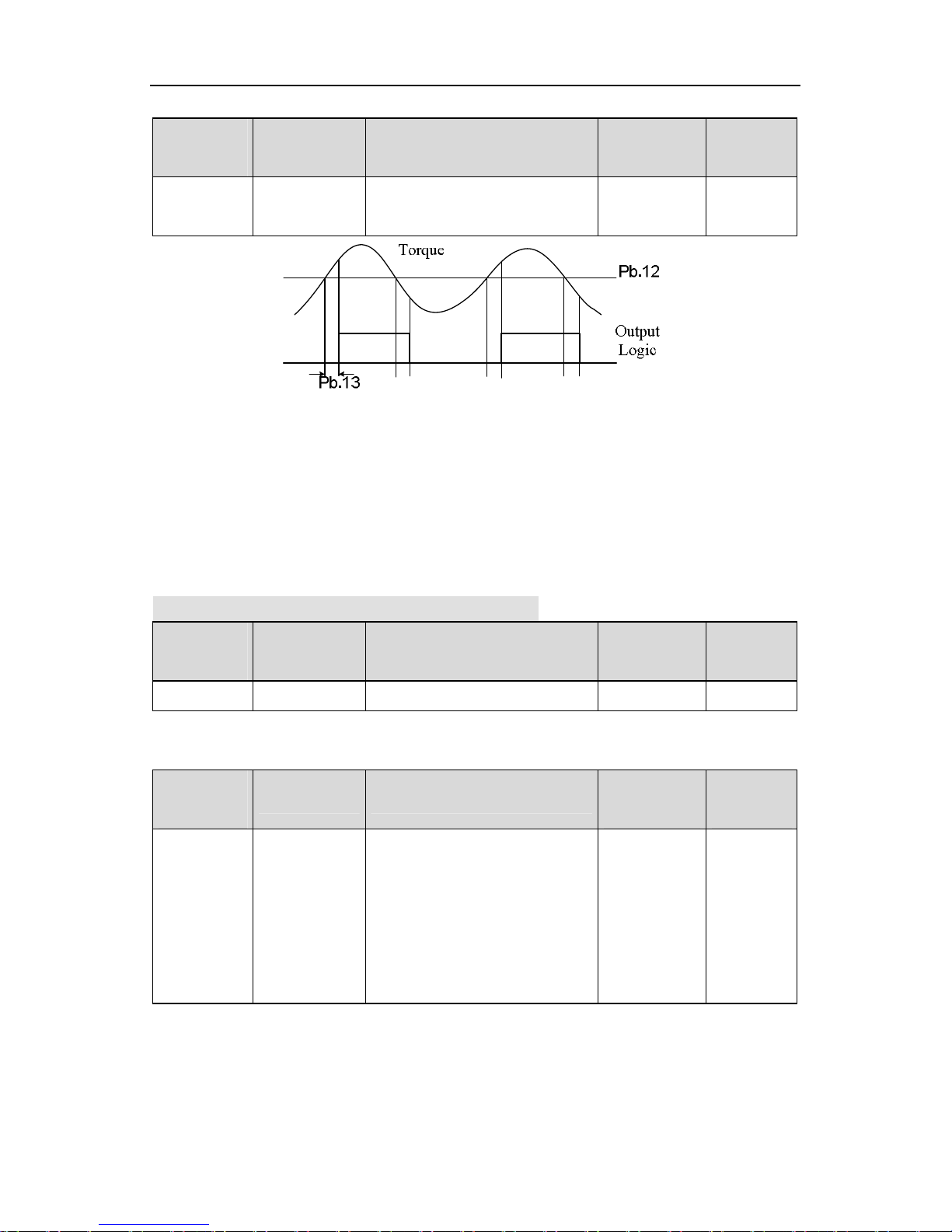
CHF100A series high performance universal inverter
.93.
This value is depending on model.
Function
Code
Name Description
Setting
Range
Factory
Setting
PB.13
D
etection time
cof overtorque
0.0~60.0s 0~60 0.1s
Figure 6.34 Overtorque control function.
If PB.11 is set to be 1or 3, and if the output torque of inverter reaches to PB.12, and with
delay of PB.13, this will output the overtorque. And the TRIP light will reflash. If P6.01
~P6.03 are set to be10, the output will be valid.
If PB.11 is set to be 2 or 4, when overtorque signal meets the output conditions, inverter
proforms warming signal OL3,and meanwhile stops the output.
6.13 PC Group--Serial Communication
Function
Code
Name Description
Setting
Range
Factory
Setting
PC.00 Local address 0~247 0~247 1
This parameter determines the slave address used for communication with master. The
value “0” is the broadcast address.
Function
Code
Name Description
Setting
Range
Factory
Setting
PC.01
Baud rate
selection
0: 1200BPS
1: 2400BPS
2: 4800BPS
3: 9600BPS
4: 19200BPS
5: 38400BPS
0~5 4
This parameter can set the data transmission rate during serial communication.
Notice: The baud rate of master and slave must be the same.

CHF100A series high performance universal inverter
Communication
Communication
Communication
Function
Setting
Name Description
Code
Range
0: RTU, 1 start bit, 8 data bits,
no parity check, 1 stop bit.
1: RTU, 1 start bit, 8 data bits,
even parity check, 1 stop bit.
2: RTU, 1 start bit, 8 data bits,
odd parity check, 1 stop bit.
PC.02 Data format
0~5 1
3: RTU, 1 start bit, 8 data bits,
no parity check, 2 stop bits.
4: RTU, 1 start bit, 8 data bits,
even parity check, 2 stop bits.
5: RTU, 1 start bit, 8 data bits,
odd parity check, 2 stop bits.
This parameter defines the data format used in serial communication protocol.
Function
Setting
Name Description
Code
Range
Factory
Setting
Factory
Setting
PC.03
0~200ms 0~200 5ms
delay time
This parameter can be used to set the response delay in communication in order to
adapt to the MODBUS master. In RTU mode, the actual communication delay should be
no less than 3.5 characters’ interval.
Function
Setting
Factory
Name Description
Code
Range
Setting
0.0: Disabled
PC.04
timeout delay
0.1~100.0s
0.0~100.0
0.0s
When the value is zero, this function will be disabled. When communication interruption
is longer than the non-zero value of PC.04, the inverter will alarm communication error
(CE).
Function
Setting
Factory
Name Description
Code
Range
Setting
0: Alarm and coast to stop
1: No alarm and continue to
PC.05
error action
run
0~3 1
2: No alarm but stop
.94.

CHF100A series high performance universal inverter
Function
Name Description
Code
according to P1.06 (if
P0.01=2)
3: No alarm but stop
according to P1.06
0: When communication error occurs, inverter will alarm (CE) and coast to stop.
1: When communication error occurs, inverter will omit the error and continue to run.
2: When communication error occurs, if P0.01=2, inverter will not alarm but stop
according to stop mode determined by P1.06. Otherwise it will omit the error.
3: When communication error occurs, inverter will not alarm but stop according to stop
mode determined by P1.06.
Function
Name Description
Code
Unit’s place of LED
0: Response to writing
Setting
Range
Setting
Range
Factory
Setting
Factory
Setting
1: No response to writing
PC.06
Response
action
A stands for: Unit’s place of LED.
B stands for: Ten’s place of LED
Ten’ s place of LED
0: Reference not saved when
power off
1: Reference saved when
power off
Figure 6.35 Meaning of PC.06.
00~11 00
.95.

CHF100A series high performance universal inverter
6.14 PD Group--Supplementary Function
Function
Name Description
Code
PD.00-PD.09 Reserved
Setting
Range
Factory
Setting
6.15 PE Group—Factory Setting
This group is the factory-set parameter group. It is prohibited for user to access.
.96.


CHF100A series high performance universal inverter
Fault
Fault Type Reason Solution
Code
DC bus
UV
Under-voltage
OL1 Motor overload
1.Open phase occurred with
power supply.
2.Momentary power loss
occurred
3.Wiring terminals for input
power supply are loose.
4.Voltage fluctuations in
power supply are too large.
1. Motor drive heavy load at
low speed for a long time.
2. Improper V/F curve
3. Improper motor’s overload
protection threshold (PB.03)
4. Sudden change of load.
Inspect the input power
supply or wiring.
1. Select variable
frequency motor.
2. Check and adjust
V/F curve.
3. Check and adjust
PB.03
4. Check the load.
OL2
SPI
Inverter
overload
Input phase
failure
1. Load is too heavy or
Acc/Dec time is too short.
2. Improper V/F curve
3. Capacity of inverter is too
small.
1.Open-phase occurred in
power supply.
2.Momentary power loss
occurred.
3. Wiring terminals for
input power supply are
loose.
4.Voltage fluctuations in
power supply are too large.
1. Increase Acc/Dec
time or select bigger
capacity inverter.
2. Check and adjust
V/F curve.
3. Select bigger
capacity inverter.
Check the wiring,
installation and power
supply.
5.Voltage balance between
phase is bad.
.98.

 Loading...