

Inverium TB-7Z-020-EMC Hardware User Manual

TB-7Z-020-EMC Hardware User Manual
1
Rev.
1.02
TB-7Z-020-EMC
Hardware User Manual
Rev.1.02

TB-7Z-020-EMC Hardware User Manual
2
Rev.
1.02
Revision History
Version Date Description Publisher
Rev 1.00 2013/01/31 Release Version Yoshioka
Rev 1.01 2013/04/25 Modified Table 7-17 and some typos. Yoshioka
Rev.1.02 2013/11/13 Modified 7.17 (Description of J6 and J7 was reverse) Kiguchi

TB-7Z-020-EMC Hardware User Manual
3
Rev.
1.02
Table of Contents
1. Related Documents and Accessories ......................................................................................... 9
2. Overview ...................................................................................................................................... 9
3. Feature ........................................................................................................................................ 9
4. Block Diagram ........................................................................................................................... 10
5. External View of the Board ............................................................... ................................ .......... 11
6. Board Specifications .................................................................................................................. 12
7. Description of Components ....................................................................................................... 15
7.1. Power Supply Structure ............................................................................................................ 15
7.1.1. DC Jack Connector and Power Switch cable ................................................................... 15
7.1.2. FP_VCCO_ADJ SEL Jumper ........................................................................................... 16
7.1.3. VCC_ADJ SEL Jumper ..................................................................................................... 16
7.2. Clock System ........................................................................................................................... 17
7.3. On-board PLL ........................................................................................................................... 18
7.4. I2C BUS.................................................................................................................................... 19
7.5. Memory..................................................................................................................................... 20
7.5.1. DDR3 ................................................................................................................................ 20
7.5.2. QSPI Flash ....................................................................................................................... 21
7.5.3. SD Card Interface ............................................................................................................. 21
7.6. 10/100/1000 Ethernet PHY ...................................................................................................... 22
7.7. UART Interface ......................................................................................................................... 23
7.7.1. RS-232C Cable p in assign ............................................................................................... 23
7.8. CAN BUS.................................................................................................................................. 24
7.8.1. Termination of CAN Bus ................................................................................................... 24
7.8.2. CAN Cable pin assign ....................................................................................................... 24
7.9. USB OTG ................................................................................................................................. 25
7.9.1. USB VBUS Power Supply SEL Jumper............................................................................ 25
7.10. RTC ...................................................................................................................................... 26
7.11. Pmod .................................................................................................................................... 27
7.11.1. Pmod Power Supply SEL Jumper .................................................................................... 27
7.12. Mictor 38 ............................................................................................................................... 28
7.12.1. VTREF SEL Jumper ......................................................................................................... 29
7.13. Reset Switch ......................................................................................................................... 31
7.14. JTAG ..................................................................................................................................... 31
7.15. DVI Output ............................................................................................................................ 32
7.16. FMC Connector Interface ............................................................................................... ...... 33
7.16.1. FMC Low-Pin Count Mezzanine Card (CN4) connector. .................................................. 34
7.16.2. FMC Low-Pin Count Carrier Card (CN5) connector. ....................................................... . 36
7.17. Jumper .................................................................................................................................. 38
7.17.1. Boot Mode Settings .......................................................................................................... 39
7.17.2. JTAG Mode Setting ........................................................................................................... 39
7.18. LED ....................................................................................................................................... 40
7.19. Push Switch .......................................................................................................................... 41
7.20. Dip Switches ......................................................................................................................... 42
8. Default Settings ......................................................................................................................... 43

TB-7Z-020-EMC Hardware User Manual
4
Rev.
1.02
List of Figures
Figure 4-1 Block Diagram ................................................................................................................ 10
Figure 5-1 Component Side .............................................................................................................. 11
Figure 5-2 Solder Side ...................................................................................................................... 11
Figure 6-1 Board Dimensions (inclusive of wastable substrate, top view) ....................................... 13
Figure 6-2 Board Dimensions (inclusive of wastable substrate, bottom view) ................................. 14
Figure 7-1 Power Supply Structure .................................................................................................. 15
Figure 7-2 DC Jack Connector and Power Switch Cable ................................................................ 15
Figure 7-3 FP_VCCO_ADJ SEL Jumper ......................................................................................... 16
Figure 7-4 VCC_ADJ SEL Jumper ................................................................................................... 16
Figure 7-5 Clock System Diagram ................................................................................................... 17
Figure 7-6 5V49EE504 EEPROM PROGRAMABLE CLOCK GENERATOR .................................. 18
Figure 7-7 I2C Bus Topology ............................................................................................................ 19
Figure 7-8 DDR3 Memory Connection ............................................................................................. 20
Figure 7-9 QSPI Connection ............................................................................................................ 21
Figure 7-10 SD Card Slot Connection .............................................................................................. 21
Figure 7-11 micro SD CARD Socket ................................................................................................ 21
Figure 7-12 RGMII Connection ........................................................................................................ 22
Figure 7-13 RJ-45 internal LED ....................................................................................................... 22
Figure 7-14 UART Connection ......................................................................................................... 23
Figure 7-15 RS-232C/CAN Cable connection ................................................................................. 23
Figure 7-16 CAN Connection ........................................................................................................... 24
Figure 7-17 CN15 and CAN Termination ......................................................................................... 24
Figure 7-18 USB Connection ........................................................................................................... 25
Figure 7-19 USB VBUS Power Supply S EL Jumper........................................................................ 25
Figure 7-20 RTC Connecti on ........................................................................................................... 26
Figure 7-21 Pmod Connection ......................................................................................................... 27
Figure 7-22 Pmod Port’s Power SEL Jumper .................................................................................. 27
Figure 7-23 MICTOR 38 Connection ............................................................................................... 28
Figure 7-24 ARM PJTAG Port’s VTREF SEL Jumper ...................................................................... 29
Figure 7-25 XC7Z020's System Reset Push Switch ........................................................................ 31
Figure 7-26 JTAG Connection .......................................................................................................... 31
Figure 7-27 DVI Connection ............................................................................................................. 32
Figure 7-28 FMC LPC Pin List ......................................................................................................... 33
Figure 7-29 Jumpers Position .......................................................................................................... 38
Figure 7-30 LED Position ................................................................................................................. 40
Figure 7-31 Push Switches .............................................................................................................. 41
Figure 7-32 DIP Switch Position ...................................................................................................... 42

TB-7Z-020-EMC Hardware User Manual
5
Rev.
1.02
List of Tables
Table 7-1 Power Setting ................................................................................................................... 16
Table 7-2 Clock signals pin assign ................................................................................................... 17
Table 7-3 External PLL settings ........................................................................................................ 18
Table 7-4 I2C Address Map .............................................................................................................. 19
Table 7-5 RJ-45 internal LED Func tion Table................................................................................... 22
Table 7-6 RS-232C Cable pin assign ............................................................................................... 23
Table 7-7 CAN BUS Cable pin assign .............................................................................................. 24
Table 7-8 USB Settings .................................................................................................................... 25
Table 7-9 RTC I2C Address.............................................................................................................. 26
Table 7-10 Pmod pin assign ............................................................................................................. 27
Table 7-11 Pmod Power Setting ....................................................................................................... 27
Table 7-12 JTAG Mode Setting for Mictor-38 ................................................................................... 28
Table 7-13 Jumper Function Table ................................................................................................... 29
Table 7-14 MICTOR 38 pin assignment ........................................................................................... 30
Table 7-15 JTAG(CN12) Pin assign ................................................................................................. 31
Table 7-16 DVI TX pin assign ........................................................................................................... 32
Table 7-17 FMC LPC MC Connector pin assignment table (CN4) .................................................. 34
Table 7-18 FMC LPC CC Connector pin assignment table (CN5) ................................................... 36
Table 7-19 All Jumpers Function Table ............................................................................................ 38
Table 7-20 Boot Mode Settings ........................................................................................................ 39
Table 7-21 JTAG Mode Setting ........................................................................................................ 39
Table 7-22 LED Function Table ........................................................................................................ 40
Table 7-23 Push Switch Function Table ........................................................................................... 41
Table 7-24 Dip Switch Function Table .............................................................................................. 42
Table 8-1 Default Jumper Settings ................................................................................................... 43
Table 8-2 Default Switch Settings .................................................................................................... 43
TB-7Z-020-EMC Hardware User Manual
6
Rev.
1.02
!
Introduction
Thank you for purchasing the TB-7Z-020-EMC board. Before using the product, be sure to carefully
read this user manual and fully understand how to correctly use the product. First read through this
manual, then always keep it handy.
Observe the precautions listed below to prevent injuries to you or other personnel or damage to property.
Before using the product, read these safety precautions carefully to assure correct use.
These precautions contain serious safety instructions that must be observed.
After reading through this manual, be sure to always keep it handy.
The following conventions are used to indicate the possibility of injury/damage and classify precautions if
the product is handled incorrectly.
SAFETY PRECAUTIONS Be sure to observe these precautions
Danger
Warning
Caution
Indicates the high possibility of serious injury or death if the product is handled
incorrectly.
Indicates the possibility of serious injury or death if the product is handled
incorrectly.
Indicates the possibility of injury or physical d am age in connection with houses or
household goods if the product is handled incorrectly.
The following graphical symbols are used to indicate and classify precautions in this manual.
(Examples)
Turn off the power switch.
Do not disassemble the product.
Do not attempt this.
TB-7Z-020-EMC Hardware User Manual
7
Rev.
1.02
!
! !
!
!
!
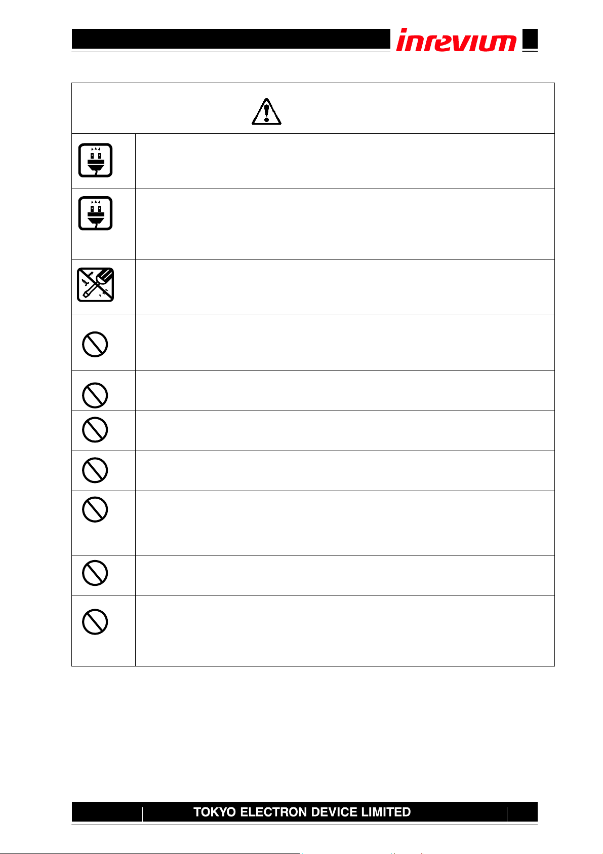
Warning
In the event of a failure, disconnect the power supply.
If the product is used as is, a fire or electric shock may occur. Disconnect the power supply
immediately and contact our sales personnel for repair.
If an unpleasant smell or smoking occurs, disconnect the power supply.
If the product is used as is, a fire or electric shock may occur. Disconnect the power supply
immediately. After verifying that no smoking is observed, contact our sales personnel for
repair.
Do not disassemble, repair or modify the product.
Otherwise, a fire or el ectric shock may occur due to a short circuit or heat generation. For
inspection, modification or repair, contact our sales personnel.
Do not touch a cooling fan.
As a cooling fan rotates in high speed, do not put your hand close to it. Otherwise, it may
cause injury to persons. Never touch a rotating cooling fan.
Do not place the product on unstable locations.
Otherwise, it ma y drop or fall, resulting in injury to persons or failure.
If the product is dropped or damaged, do not use it as is.
Otherwise, a fire or electric shock may occur.
Do not touch the product with a metallic object.
Otherwise, a fire or electric shock may occur.
Do not place the product in dusty or humid locations or where water may
splash.
Otherwise, a fire or elec tric shock may occur.
Do not get the product wet or touch it with a wet hand.
Otherwise, the product may break down or it may cause a fire, smoking or electric shock.
Do not touch a connector on the product (gold-plated portion).
Otherwise, the surface of a connector may be contaminated with sweat or skin oil, resulting
in contact failure of a connector or it may caus e a malfunction, fire or electric shock due to
static electricity.
TB-7Z-020-EMC Hardware User Manual
8
Rev.
1.02
!
!
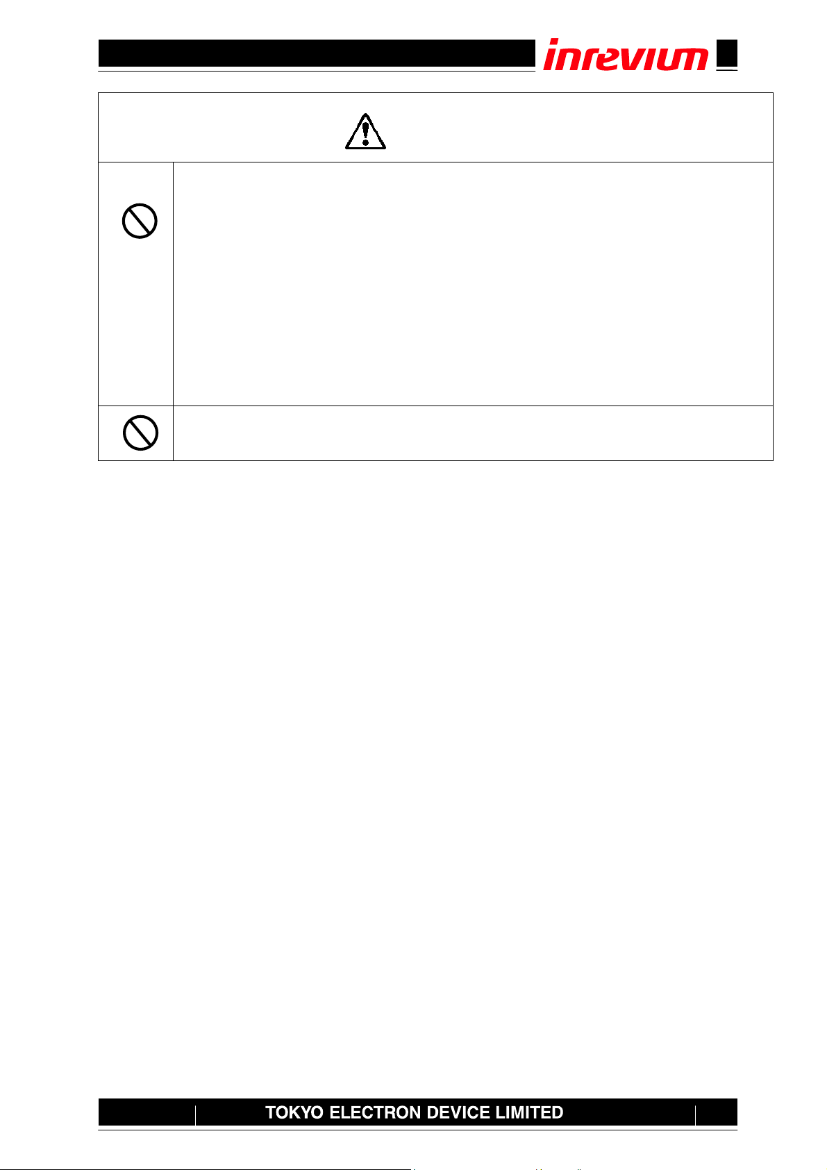
Caution
Do not use or place the product in the following locations.
Humid and dusty locations
Airless locations such as closet or bookshelf
Locations which receiv e oily smoke or steam
Locations exposed to direct sunlight
Locations close to heating equipment
Closed inside of a car where the temperature becomes high
Staticky locations
Locations close to water or chemicals
Otherwise, a fire, electric shock, accident or deformation may occur due to a short circuit or heat
generation.
Do not place heavy things on the product.
Otherwise, the product may be damaged.
Disclaimer
This product is an evaluation board for Xilinx Zynq AP SoC FPGA. Tokyo Electron Device Limited
assumes no responsibility for any damages resulting from the use of this product for purposes other than
those stated.
Even if the product is used properly, Tokyo Electron Device Limited assumes no responsibility for any
damages caused by:
(1) Earthquake, thunder, natural disaster or fire resulting from the use beyond our responsibility, acts by
a third party or other accidents, the customer’s willful or accidental misuse or use under other
abnormal conditions.
(2) Secondary impact arising from use of this product or its unusable state (business interruption or
others)
(3) Use of this product against the instructions giv en in this manual.
(4) Malfunctions due to connection to other devices.
Tokyo Electron Device Limited assumes no responsibility or liability for:
(1) Erasure or corruption of data arising from use of this product.
(2) Any consequences or other abnormalities arising from use of this product, or
(3) Damage of this product not due to our responsibility or failure due to modification
This product has been developed by assuming its use for research, testing or evaluation. It is not
authorized for use in any system or application that requires high reliability.
Repair of this product is carried out by replacing it on a chargeable basis, not repairing the faulty devices.
However, non-chargeable replacement is offered for initial failure if such notification is received within
two weeks after delivery of the product.
The specification of this product is subject to change without prior notice.
The product is subject to discontinuation without pr ior notice.

TB-7Z-020-EMC Hardware User Manual
9
Rev.
1.02
1. Related Documents and Accessories
Related documents:
All documents relating to this board can be downloaded from our website. Please see attached paper on
the products.
Accessories.
- RS-232C/CAN Bus Cable x1
- microSD card 4GB x1
- Power Supply(DC-12V) x1
- DC Switch Cable x1
- Spacer Set
2. Overview
The TB-7Z-020-EMC evaluation board for the Zynq™-7000 All Programmable SoC provides a hardware
environment for developing and evaluating designs targeting the Zynq™-7000 XC7Z020-1CLG484. The
TB-7Z-020-EMC provides features common to many embedded processing systems, including DDR3
SDRAM component memory, a 10/100/1000 Ethernet PHY, general purpose I/O, a DVI Transm itter, a
USB OT G 2.0 Port, a Pmod interface, a CAN interface and a UART interface. Other features can be
supported using VITA-57 FPGA mezzanine cards (FMC) attached to either of two low pin count (LPC)
FMC connectors.
3. Feature
Zynq-7000: Xilinx XC7Z020-1CLG484
Memory: 1GByte (32Mword x 32bit x 8banks) DDR3 SDRAM Com ponent
128Mbit Quad SPI Flash
Secure Digital Card (Connector)
Ethernet PHY: Marvell’s 88E1518-XX-NNB2C000 RGMII Interface with RJ45
USB OTG 2.0 Transceiver: TI’s TUSB1210BRHB *1
DVI Complaint Transmitter: TI’s TFP410PAP
RS232 Transceiver: TI’s MAX3232CPW with 2.0 pitch PinHeader*2
FMC Connector: Samtec’s ASP-134604-01 (FMC LPC MC) mounted on bottom side*3
Samtec’s ASP-134603-01 (FMC LPC CC) mounted on top side*3
Cation: FMC connetors a re only exclusice use
CAN Bus Transceiver: PHILIPS’s T XS0104EPWR with 2.0 pitch PinHeader*2
Pmod Connector: Digilent Pmod™ compatible headers (2x6)
JTAG Port: Standard Xilinx JTAG Interface with 14-pin 2.0 pitch PinHeader
ARM JTAG + Logic Analyzer function Interface with Mictor-38 Connector
SD Card: microSD Card connector
Oscillators: Fixed 33.33333MHz LVCMOS oscillator
Clock Generator: IDT’s 5V49EE504NLGI
Note *1: TUSB1210 and Zynq-7000 have a timing incompatibility at hot temperature.
Please use TB-7Z-020-EMC at room temperature.
Note *2: Rs-232C and CAN interfaces are connecting by accessory cable.
Note *3: FMC connetors are only exclusice use.
TB-7Z-020-EMC Hardware User Manual
10
Rev.
1.02
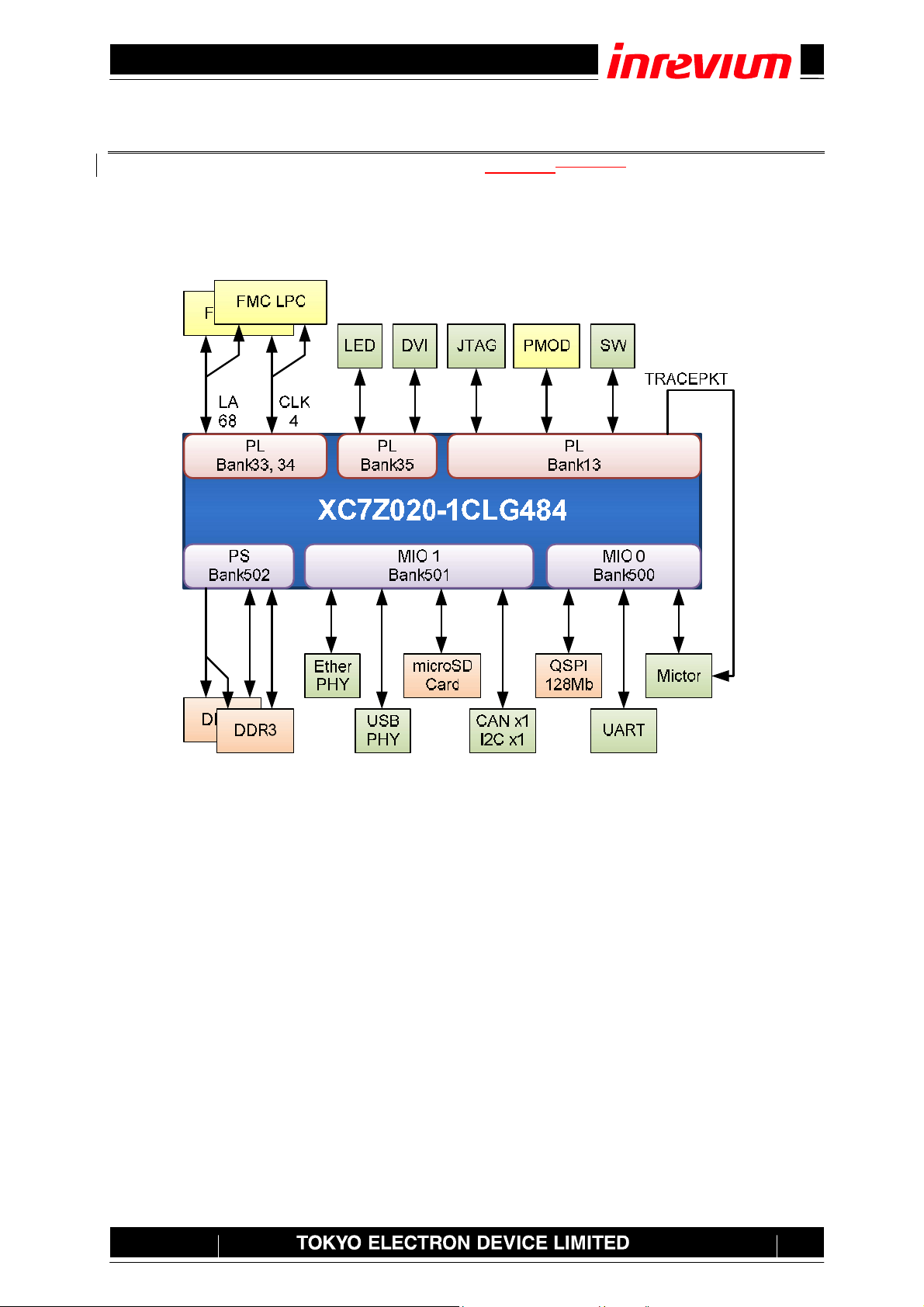
4. Block Diagram
The TB-7Z-020-EMC board block diagram is s hown in Figure 4-1Figure 4-1.
PS block is connecting specific memories or interfaces.
PL block is connecting FMC conne ctor and debug interfaces.
For more detail, please refer to each peripheral section
.
Address
Data16bit
Data16bit
Figure 4-1 Block Diagram
TB-7Z-020-EMC Hardware User Manual
11
Rev.
1.02
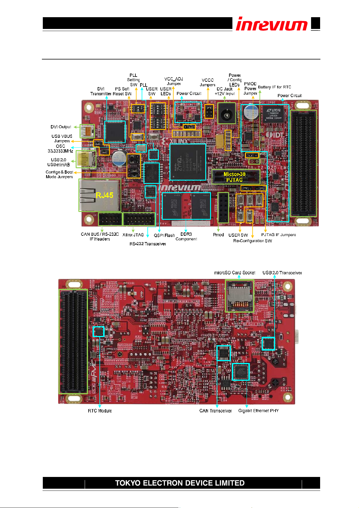
5. External View of the Board
The TB-7Z-020-EMC board external view is shown in Figure 5-1 and Figure 5-2.
FMCLPCCC
Figure 5-1 Component Side
FMCLPCMC
Figure 5-2 Solder Side

TB-7Z-020-EMC Hardware User Manual
12
Rev.
1.02
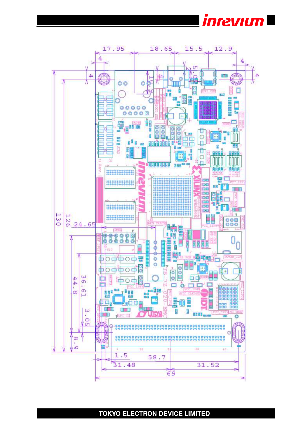
6. Board Specifications
The TB-7Z-020-EMC board specifications are showed in Figure 6-1 and Figure 6-2.
External Dimensions: 130 mm (W) x 69 mm (H)
Number of Layers: 12 layers
Board Thickness: 1.6 mm
Material: FR-4
FMC LPC CC Connector: Samtec’s ASP-134603-01
FMC LPC MC Connector: Samtec’s ASP-134604-01
USB OTG Connector: Molex’s 67803-8020
RJ-45 connector: HanRun’s HR911130C
CAN & RS-232 connector: one 2.0-pitch Header (2x5)
HDMI/DVI Video connector: Molex’s 046765-1001
Pmod connector: Samtec’s SSW-106-01-F -D
MICTOR Connector: TE Connectivity’s 2-5767004-2
SD Card Slot: JAE’s ST1W008S4ER1500
Xilinx JTAG connector: Molex’s 87832-1420
Power Input connector: CUI Inc’s PJ-006A
TB-7Z-020-EMC Hardware User Manual
13
Rev.
1.02
Figure 6-1 Board Dimensions (inclusive of wastable substrate, top view)

TB-7Z-020-EMC Hardware User Manual
14
Rev.
1.02
Figure 6-2 Board Dimensions (inclusive of wastable substrate, botto m view)
 Loading...