

Page 1

ISM4343-WBM-L151-EVB Specification
DOC-DS-20077-2
Confidential Inventek Systems
Page 1
INVENTEK SYSTEMS
ISM4343-WBM-L151-EVB
Evaluation Board
EVB User’s Manual
802.11 b/g/n + 4.2 BT/BLE + Cortex M4
Page 2

ISM4343-WBM-L151-EVB Specification
DOC-DS-20077-2
Confidential Inventek Systems
Page 2
Table of Contents
1 PART NUMBER DETAIL DESCRIPTION .......................................................................... 3
1.1 Ordering Information ...................................................................................................... 3
2 OVERVIEW ........................................................................................................................... 3
3 FEATURES ............................................................................................................................ 4
3.1 Limitations ...................................................................................................................... 5
4 COMPLEMENTARY DOCUMENTATION ........................................................................ 6
4.1 EVB................................................................................................................................. 6
5 BLOCK DIAGRAM ............................................................................................................... 6
6 INTRODUCTION .................................................................................................................. 7
6.1 Applications .................................................................................................................... 7
7 FEATURES ............................................................................................................................ 8
7.1 Feature List ..................................................................................................................... 8
7.2 EVB Hardware layout and configuration ....................................................................... 9
7.3 Top View ...................................................................................................................... 10
7.4 Bottom View ................................................................................................................. 11
8 Power Supply ........................................................................................................................ 12
8.1 The ISM4343-WBM-L151-EVB is designed to be powered by a 5 V DC power
supply. 12
8.2 Reset Source.................................................................................................................. 12
8.3 Audio............................................................................................................................. 12
8.4 UART ............................................................................................................................ 13
8.5 Timer ............................................................................................................................. 13
8.6 I2C................................................................................................................................. 13
8.7 ADC .............................................................................................................................. 13
8.8 I2S ................................................................................................................................. 13
8.9 SPI ................................................................................................................................. 13
8.10 Quad SPI ....................................................................................................................... 14
8.11 BT GPIO ....................................................................................................................... 14
9 Connectors ............................................................................................................................ 14
9.1 Power Supply Connector (Micro USB: P1) .................................................................. 14
9.2 Boot0 Configure PIN Header (JP7) .............................................................................. 15
9.3 Boot1 Configure PIN Header (JP9) .............................................................................. 15
9.4 Power source ................................................................................................................. 15
9.5 Function PIN Header .................................................................................................... 16
9.6 BT PCM interface PIN Header ..................................................................................... 18
10 Schematic .............................................................................................................................. 19
10.1 ISM4343-M4G-L151 Application schematic ................................................................. 19
10.2 Schematic for Power ..................................................................................................... 20
10.3 Schematic for USB to URAT, JTAG,& MCU Make Up ............................................. 21
10.4 Comparing eS-WiFi pinouts on our standard pinouts .................................................. 21
11 REVISION CONTROL ........................................................................................................ 23
12 CONTACT INFORMATION ............................................................................................... 23
Page 3
ISM4343-WBM-L151-EVB Specification
DOC-DS-20077-2
Confidential Inventek Systems
Page 3
1 PART NUMBER DETAIL DESCRIPTION
1.1 Ordering Information
Device
Description
Ordering Number
ISM4343-WBM-L151-EVB
2.4 Wi-Fi + BT/BLE +
Cortex M4 EVB
ISM4343-WBM-L151-EVB
2 OVERVIEW
The Inventek ISM4343-WBM-L151-EVB is a single-band IEEE 802.11n-compliant
MAC/PHY, BT 4.1 radio and ST Micro STM32F412 MCU Evaluation Board platform.
Channel bandwidth of 20MHz is supported for IEEE 802.11n traffic. 2.4GHz internal
power amplifiers and a Power Management Unit (PMU), with one switching regulator.
The ISM4343-WBM-L151-EVB integrates clock, Wi-Fi/BT and front end into the smallest
form factor LGA Module. The ISM4343-WBM-L151-EVB IEEE 802.11 b/g/n enables
wireless connectivity to the simplest existing sensor products with minimal engineering
effort. ISM4343-WBM-L151-EVB reduces development time, lowers manufacturing costs,
saves board space, simplifies certification compliance, and minimizes customer RF
expertise required during development of target applications.
The ISM4343-WBM-L151-EVB provides the highest level of integration for a wireless
system, with integrated single band Wi-Fi and BT/BLE based on Cypress’ IEEE802.11
b/g/n single-stream and BT/BLE 4.1 with support for antenna diversity and provisions for
supporting future specifications. The ISM4343-WBM-L151-EVB also supports BT 4.2LE
Secure Connection via the Cypress stack. Integrated power amplifiers, LNAs and T/R
switches for the 2.4 GHz WLAN band, are also included, greatly reducing the external
part count, PCB footprint, and cost of the solution.
The ISM4343-WBM-L151-EVB small form-factor solution also minimizes external
components to drive down cost for mass volumes and allows for handheld device flexibility in
size, form and function. Comprehensive power management circuitry and software ensure
the system can meet the needs of high mobile devices that require minimal power
consumption and reliable operations.
Page 4

ISM4343-WBM-L151-EVB Specification
DOC-DS-20077-2
Confidential Inventek Systems
Page 4
The ISM4343-WBM-L151-EVB module includes an ST Micro STM32F412 Cortex M4
MCU. SPI and UART interfaces enable easy connection to an embedded design. The
ISM4343-WBM-L151-EVB module requires no operating system. The ISM4343-WBML151-EVB module also fully supports Cypress’ WICED Platform SDK.
The ISM4343-WBM-L151-EVB is compatible with the Bluetooth Low Energy operating
mode, which provides a dramatic reduction in the power consumption of the Bluetooth
radio and baseband. The primary application for this mode is to provide support for low
data rate devices, such as sensors and remote controls.
The ISM4343-WBM-L151-EVB implements the highly sophisticated Enhanced
Collaborative Coexistence algorithms and hardware mechanisms, allowing for an
extremely collaborative Bluetooth coexistence scheme along with coexistence support
for external radios such as cellular and LTE, GPS, and Ultra-Wideband. An
independent, high-speed UART is provided for the Bluetooth host interface.
3 FEATURES
The ISM4343-WBM-L151-EVB supports the following WLAN, Bluetooth & MCU
functions:
• STM32 ARM 32-bit CortexTM-M4 with a frequency up to 100 MHz
o 1 Mbyte of MCU internal Flash
o 256KB of SRAM
o SPI, Quad SPI (support Dual mode), USART, PCM
o ADC, I2C, I2S, GPIO, Timers
o JTAG
• Single-band 2.4 GHz b/g/n, 802.11b, 802.11g, 802.11n (single stream)
o IEEE 802.11b 1 – 11 Mbps
o IEEE 802.11g 6 – 54 Mbps
o IEEE 802.11n (2.4 GHz) 7.2 – 150Mbps
• Support BT COEX
• Cypress WICED Fully compatible
• IEEE 802.11b/g/n single-band radio with internal Power Amplifiers, LNAs and T/R
switches
• Hardware Encryption WEP, WPA/WPA2
• Modulation Modes include:
o WiFi: CCK and OFDM with BPSK, QPSK, 16 QAM, 64QAM, 256QAM
o BT: Dual-mode classic Bluetooth and Classic Low Energy operation
• Concurrent Bluetooth and WLAN operation
• Single antenna support
Page 5

ISM4343-WBM-L151-EVB Specification
DOC-DS-20077-2
Confidential Inventek Systems
Page 5
• Supports a single 2.4 GHz antenna shared between WLAN and Bluetooth
• BT host digital interface (can be used concurrently with above interface):
o UART (up to 4 Mbps)
• Bluetooth v4.1 with integrated Class 1 PA
• Bluetooth 2.1+EDR, Bluetooth 3.0, Bluetooth 4.1 (Bluetooth Low Energy)
• Bluetooth v4.2LE Secure Connection via the Cypress BSA stack.
• ECI – enhanced coexistence support, ability to coordinate BT SCO transmissions
around WLAN receives
• I²S/PCM for BT audio
• HCI high-speed UART (H4, H4 +, H5) transport support
• Bluetooth low power inquiry and page scan
• Bluetooth Low Energy (BLE) support
The BBC supports all Bluetooth 4.0 features, with the following benefits:
• Dual-mode classic Bluetooth and classic Low Energy (BT and BLE) operation.
• Low Energy Physical Layer
• Low Energy Link Layer
• Enhancements to HCI for Low Energy
• Low Energy Direct Test mode
• AES encryption
3.1 Limitations
Inventek Systems products are not authorized for use in safety-critical applications
(such as life support) where a failure of the Inventek Systems product would
reasonably be expected to cause severe personal injury or death.
Page 6
ISM4343-WBM-L151-EVB Specification
DOC-DS-20077-2
Confidential Inventek Systems
Page 6
4 COMPLEMENTARY DOCUMENTATION
4.1 EVB
➢ Evaluation Board
o Evaluation Board Specification
o EVB User’s Guide
o Design Guidelines
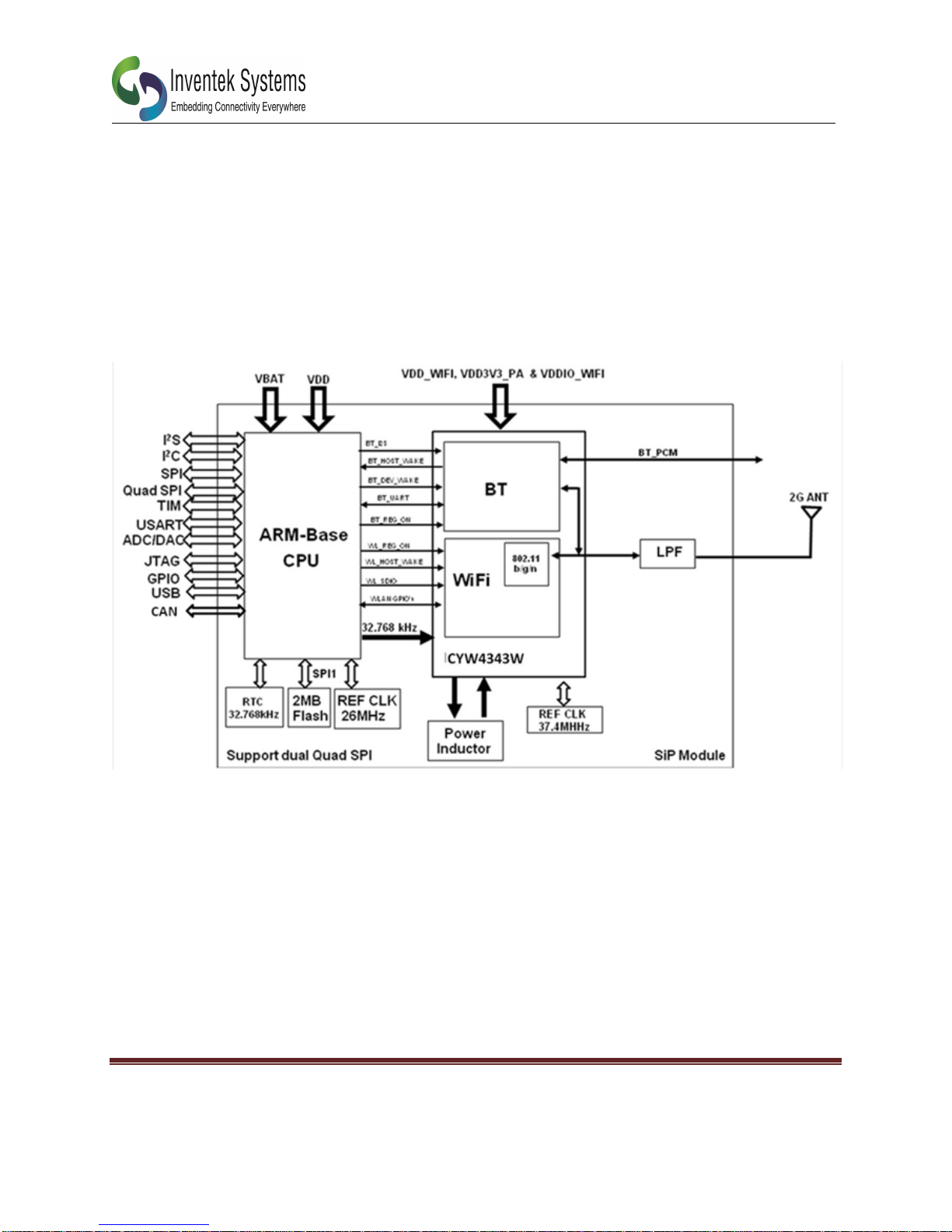
5 BLOCK DIAGRAM
Figure 1: ISM4343-WBM-L151 Module Block Diagram
• ADC: Analog to Digital Converter
• I2C: Intelligent Interface Controller
• SPI: Serial Peripheral Interface
• Quad SPI: Quad Serial Peripheral Interface
• USART: Universal Synchronous/Asynchronous Receiver Transmitters
• TIM: Timers
• I2S: Inter-integrated Sound
• CAN: Controller Area Network
Page 7
ISM4343-WBM-L151-EVB Specification
DOC-DS-20077-2
Confidential Inventek Systems
Page 7
Figure 2: ISM4343-WBM-L151-EVB
6 INTRODUCTION
6.1 Applications
Applications developed using the ISM4343-WBM-L151-EVB and WICED SDK are
downloaded via USB (or optionally via USB-JTAG J-Link) to the ISM4343-WBM-L151 on
the ISM4343-WBM-L151-EVB.
Page 8

ISM4343-WBM-L151-EVB Specification
DOC-DS-20077-2
Confidential Inventek Systems
Page 8
7 FEATURES
7.1 Feature List
The ISM4343-WBM-L151-EVB provides a platform for the design and development of
applications the run on a ISM4343-WBM-L151.
Feature
Detail
ISM4343-WBM-L151
The ISM4343-WBM-L151 includes and STM32F412 host microprocessor, and
Cypress WiFi/BT Chip
- STM32F412:
ARM-based 32-bit 100MHz, Flash memory up to 512kbyte, Up to 128 Kbytes
of system SRAM.
- Cypress WiFI /BT Chip”
Single chip IEEE802.11 b/g/n, Bluetooth 4.1 + HS
ISM4343-WBM-L151EVB
The is a complete WiFi / BT and networking solution and includes ISM4343-WBML151 Module, RF SMA connector and power supply
Program & Debug
Interface
Applications are downloaded to the STM32F412 host and debugged using either
USB-JTAG interface or a J-Link JTAG interface
USB-Serial UART
Interface
A UART on the STM32 host microprocessor connects to the EVB USB-serial
interface to enable serial communications with a PC terminal application
Expansion Header
The expansion header facilitates custom sensor interfaces and expansion boards
Reset Switch
Enable manual reset of the MCU
Power Supply
The EVB may be powered directly from the USB interface or from an external +5V
power supply.
Page 9

ISM4343-WBM-L151-EVB Specification
DOC-DS-20077-2
Confidential Inventek Systems
Page 9
7.2 EVB Hardware layout and configuration
Figure 4: ISM4343-WBM-L151-EVB Block Diagram
Page 10

ISM4343-WBM-L151-EVB Specification
DOC-DS-20077-2
Confidential Inventek Systems
Page 10
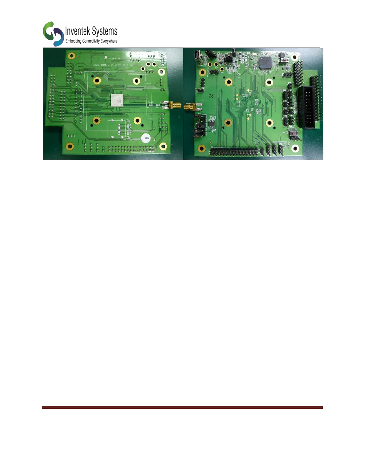
7.3 Top View
Page 11

ISM4343-WBM-L151-EVB Specification
DOC-DS-20077-2
Confidential Inventek Systems
Page 11
7.4 Bottom View
Page 12

ISM4343-WBM-L151-EVB Specification
DOC-DS-20077-2
Confidential Inventek Systems
Page 12
8 Power Supply
8.1 The ISM4343-WBM-L151-EVB is designed to be powered by a 5 V
DC power supply.
• 5 V External power source hole on the board.*(1)
• 5 V DC power with 500mA limitation from P1, the USB Micro-AB connecter
*(1) Set the jumper form pin 1-2 of JP29 to pin 2-3 of JP29 when using 5V external power
source on the ISM4343-WBM-L151-EVB. Also need connection JP27 and JP28 (Pin1 & Pin2)
Boot Option
The ISM4343-WBM-L151-EVB is able to boot from:
• Embedded user Flash.
• System memory with boot loader for ISP
• Embedded SRAM for debugging
The boot option is configured by Hardware setting for BOOT0 (JP7) and BOOT1 (JP9).
BOOT 0
BOOT 1
Boot source
0
0 or 1
ISM4343-WBM-L151 boots from User Flash (Default setting)
1 1 ISM4343-WBM-L151 boots from Embedded SRAM
1 0 ISM4343-WBM-L151 boots from System Memory
BOOT related configure
8.2 Reset Source
The reset signal of the ISM4343-WBM-L151-EVB is low active and the reset source includes:
• Reset button SW1.
• Debugging tools from JTAG connector J1.
8.3 Audio
The ISM4343-WBM-L151-EVB enables stereo audio play and microphone recording by an
external headset. An audio DAC IC is connected to both an I2S2 port and a DAC channel while
a microphone amplifier is connected to the ADC of the ISM4343-WBM-L151. The DAC IC can
be configured via I2C1.
1) Prefer usage of embedded ST-LINK/V2 to external tool connected on J1.
2) Configure MICRO_I2S2_SD GPIO in low speed (2 MHz or 10 MHz).
Page 13

ISM4343-WBM-L151-EVB Specification
DOC-DS-20077-2
Confidential Inventek Systems
Page 13
8.4 UART
The ISM4343-WBM-L151-EVB enables two channels of USART communication. One channel
(USART1) connects to R20, R23 & U3 (USB to UART IC), and Header J12 (Pin21, Pin23,
Pin25 & Pin27). Second Channel connects to header J12 (Pin20 & Pin24).
* The second channel USART overlaps to I2S function.
8.5 Timer
The ISM4343-WBM-L151-EVB enables TIMER control signal and connects to header J11.
8.6 I2C
The ISM4343-WBM-L151-EVB enables two channels of I2C function. One channel connects to
J12 (Pin2 & Pin4). Another channel connects to J12 (pin8 & Pin10).
• I2C signal traces need to be pull high.
8.7 ADC
The ISM4343-WBM-L151-EVB enables three channels of ADC signal. There are connecting to
J12 (Pin28 ~ Pin30).
8.8 I2S
The ISM4343-WBM-L151-EVB enables I2S function. The function is connecting to J12 (Pin14,
Pin16, Pin18, & Pin20).
* The I2S is overlap to USART6 function.
8.9 SPI
The ISM4343-WBM-L151-EVB enables two channels of SPI function. The First channel
connects to J12 ((Pin1, Pin13, Pin5, & Pin7). The Second channel connects to J12 (Pin11, Pin13,
Pin15, & Pin17).
* SPI1 is connected internally to Flash.
Page 14

ISM4343-WBM-L151-EVB Specification
DOC-DS-20077-2
Confidential Inventek Systems
Page 14
8.10 Quad SPI
The ISM4343-WBM-L151-EVB enables two channels of QUAD SPI function. The First channel
connects to J11 ((Pin1, Pin4, Pin5, Pin14, & pin24). The Second channel connects to J11 (Pin6,
Pin7, Pin12, Pin17, & Pin25).
8.11 BT GPIO
The BT GPIO function is connected to J20 (Pin1, Pin2, & Pin3).
9 Connectors
9.1 Power Supply Connector (Micro USB: P1)
The ISM4343-WBM-L151-EVB can be powered from 5V DC power supply via the external
Mini USB connector (P1) or external power supply hole.
- Micro USB Connector (P1)
Front view
Pin
Description
Pin
Description
1
VBUS (5V)
4
NC
2
D- (connect to U1 pin 7)
5
GND
3
D+(connect to U1 pin 8)
Page 15

ISM4343-WBM-L151-EVB Specification
DOC-DS-20077-2
Confidential Inventek Systems
Page 15
9.2 Boot0 Configure PIN Header (JP7)
Pin
Description
1
VDD_3V3
2
Boot0
3
GND
9.3 Boot1 Configure PIN Header (JP9)
Pin
Description
1
GND
2
Boot0
3
VDD_3V3
9.4 Power source
(JP29)
Pin
Description
1
VDD_5V-USB
2
5V to SiP
3
EXT_5V
Page 16

ISM4343-WBM-L151-EVB Specification
DOC-DS-20077-2
Confidential Inventek Systems
Page 16
9.5 Function PIN Header
The ISM4343-WBM-L151-EVB enables I2S, I2C, SPI, USART, TIM, ADC, GPIO function
J11
Pin
Description
Pin
Description
1
QUADSPI_BK1_IO1 (PF9)
2
MCIRO_GPIO_0 (PE3)
3
MCIRO_GPIO_3 (PB15)
4
QUADSPI_BK1_IO0 (PF8)
5
QUADSPI_BK1_IO2 (PF7)
6
QUADSPI_BK2_IO3 (PC5)
7
QUADSPI_BK2_IO0 (PE7)
8
QUADSPI_CLK (PB1)
9
VDD_USB
10
MCIRO_GPIO_16 (PE15)
11
MCIRO_GPIO_25 (PD10)
12
QUADSPI_BK2_IO1 (PE8)
13
MCIRO_GPIO_27 (PD8)
14
QUADSPI_BK1_NCS (PG6)
15
MCIRO_GPIO_28 (PB8)
16
MCIRO_GPIO_26 (PD1)
17
QUADSPI_BK2_NCS (PC11)
18
MCIRO_GPIO_30 (PE0)
19
MCIRO_GPIO_33 (PB13)
20
MCIRO_GPIO_32 (PB12)
21
MCIRO_GPIO_5 (PB0)
22
MCIRO_GPIO_34 (PB14)
23
PC13
24
QUADSPI_BK1_IO3 (PF6)
25
QUADSPI_BK2_IO2 (PC4)
26
NC
27
NC
28
NC
29
GND
30
GND
J12
Pin
Description
Pin
Description
1
MICRO_SPI1_NSS (PA4)
2
I2C2_SDA (PB10)
3
MICRO_SPI1_MISO (PA6)
4
I2C2_SCL (PB11)
5
MICRO_SPI1_SCK (PA5)
6
GND
7
MICRO_SPI1_MOSI (PA7)
8
I2C1_SDA (PB7)
9
GND
10
I2C1_SCL (PB6)
11
SPI4_SCK (PE12)
12
GND
13
SPI4_MOSI (PE14)
14
I2S2_SD (PC3)
15
SPI4_NSS (PE11)
16
I2S2_WS (PB9)
Page 17

ISM4343-WBM-L151-EVB Specification
DOC-DS-20077-2
Confidential Inventek Systems
Page 17
17
SPI4_MISO (PE13)
18
MICRO_I2S_DI (PE5)
19
GND
20
USART6_RX_I2S2_CK (PC7)
21
MICRO_UART1_RX (PA10)
22
GND
23
MICRO_UART1_RTS (PA12)
24
USART6_TX_I2S2_MCK(PC6)
25
MICRO_UART1_TX (PA9)
26
GND
27
MICRO_UART1_CTS (PA11)
28
MICRO_ADC_IN1 (PA1)
29
MICRO_ADC_IN3 (PA3)
30
MICRO_ADC_IN2 (PA2)
Trace debugging (JTAG) connector J1
Pin
Description
Pin
Description
1
VDD_3V3
2
VDD_3V3
3
MICRO_JTAG_TRSTN (PB4)
4
GND
5
MICRO_JTAG_TDI (PA15)
6
GND
7
MICRO_JTAG_TMS (PA13)
8
GND
9
MICRO_JTAG_TCK (PA14)
10
GND
11
RTCK
12
GND
13
MICRO_JTAG_TDO (PB3)
14
GND
15
MICRO_RST_N
16
GND
17
DBGRQ
18
GND
19
DBGACK
20
GND
RTCK can choose pull high or low (Default is setting pull low).
- JP14 -JP20
Pin
Description
1
MICRO_WKUP
2
GND
3
MICRO_RST_N
Page 18

ISM4343-WBM-L151-EVB Specification
DOC-DS-20077-2
Confidential Inventek Systems
Page 18
-J23 -J24
Pin
Description
1
SPI4_NSS
2
SPI_NSS
3
MICRO_SPI_NSS
-J25 -J26
Pin
Description
1
MICRO_SPI_SCK
2
SPI_SCK
3
SPI4_SCK
9.6 BT PCM interface PIN Header
- JP12 -JP10
Pin
Description
1
BT_PCM_OUT
2
BT_PCM_SYNC
Pin
Description
1
BT_GPIO_3
2
BT_GPIO_4
3
BT_GPIO_5
Pin
Description
1
SPI4_MISO
2
SPI_MISO
3
Pin
Description
1
2
SPI_MOSI
3
SPI4_MOSI
Pin
Description
1
BT_PCM_IN
2
GND
3
BT_PCM_CLK
Page 19

ISM4343-WBM-L151-EVB Specification
DOC-DS-20077-2
Confidential Inventek Systems
Page 19
10 Schematic
10.1 ISM4343-M4G-L151 Application schematic
VBAT
VDD_3V3
QUADSPI_BK1_IO3 1
JP8
SMA
1
1
2
2
3
3
4
4
5
5
VDD_3V3
C61 2.2uF
C48
DNI
R92
10pF
C49
DNI
C76
DNI
R103
10pF
C77
DNI
JP7
header3
1
2
3
VDD_3V3
Y1
DNI
C47
DNI
C46 DNI
C45
2.2uF
C44
2.2uF
C57 2.2uF
BT_GPIO_51
BT_GPIO_41
BT_GPIO_31
C58
2.2uF
JP9
header3
1
2
3
VDD_3V3
USART1_TX 1
USART1_CTS 1
USART1_RTS 1
USART1_RX 1
BT_PCM_OUT1
BT_PCM_IN1
BT_PCM_SYNC1
BT_PCM_CLK 1
MICRO_GPIO_261,2
QUADSPI_BK1_NCS1
VDD_USB 1
MICRO_GPIO_01
QUADSPI_BK2_MCS1
MICRO_GPIO_301
MICRO_GPIO_161
C59
2.2uF
VDD_3V3
VDD_3V3
QUADSPI_CLK1
MICRO_GPIO_51
BT_HOST_WAKE 1
QUADSPI_BK1_IO2 1
MICRO_GPIO_281
MICRO_GPIO_31
MICRO_GPIO_341
USART6_RX_I2S2_CK 1
USART6_TX_I2S2_MCK 1
QUADSPI_BK1_IO1 1
QUADSPI_BK1_IO01
MICRO_GPIO_32 1
MICRO_GPIO_33 1
I2S2_SD 1
I2S2_WS1
VDD3V3_WiFi_IO
VDD3V3_PA
MICRO_RST_N1
VDD_3V3_WIFI _IN
I2C1_SCL1
I2C2_SDA 1
I2C2_SCL 1
I2C1_SDA1
MICRO_I2S_DI1 QUADSPI_BK2_IO1 1
QUADSPI_BK2_IO0 1
SPI4_MOSI1,2
SPI4_MISO1,2
SPI4_SCK1,2
SPI4_NSS1,2
MICRO_GPIO_27 1
MICRO_GPIO_25 1
MICRO_JTAG_TMS 1
MICRO_JTAG_TRSTN 1
MICRO_JTAG_TDO 1
MICRO_JTAG_TDI 1
MICRO_JTAG_TCK 1
MICRO_WKUP1
MICRO_SPI_NSS 1,2
MICRO_ADC_IN 31
MICRO_ADC_IN 21
MICRO_ADC_IN 11
MICRO_SPI_MOSI1,2
MICRO_SPI_MISO 1,2
MICRO_SPI_SCK 1,2
QUADSPI_BK2_IO3 1
QUADSPI_BK2_IO21
PC131
C50 2.2uF
C52 2.2uF
RF_SW_CTRL1
U7
Module Pin Out
VDD3V3_WiFi
42
MCIRO_SPI2_N SS
84
GND
51
NC2
17
I2S2_WS
143
MICRO_I2S_D I
111
NC18
110
GND
27
I2C1_SCL
102
I2C1_SDA
103
GND
34
VDD3V3_WiFi_IO
28
SPI4_MOSI
14
NC24
139
MICRO_GPIO_27
86
NC3
19
MICRO_GPIO_25
87
NC25
140
NC9
88
BOOT0
104
BOOT1
79
I2S2_SD
69
USART6_RX_I2S2_C K
93
USART6_TX_I2S2_M CK
92
NC15
100
ANT
1
MCIRO_SPI2_SC K
85
NC11
95
SPI4_NSS11SPI4_SCK
12
VDD3V3_WiFi
43
I2C2_SDA
83
NC5
40
NC6
56
GND
7
I2C2_SCL
82
SPI4_MISO
13
GND
41
NC23
138
GND
49
GND
47
NC13
97
OSC32_IN
52
GND
54
OSC32_OUT
53
VDD3V3_PA
3
NC8
63
GND
23
VDD3V3_PA
4
QUADSPI_BK2_IO181QUADSPI_BK2_IO0
80
MICRO_SPI2_M ISO
21
MICRO_GPIO_28
142
MICRO_SPI_MISO
76
MICRO_WKU P
119
MICRP_GPIO_30
108
NC17
109
NC16
105
GND
15
RF_SW_CTRL
126
NC7
62
NC20
127
GND
29
QUADSPI_BK1_IO3
50
GND
18
NC12
96
MICRO_SPI2_M OSI
22
NC14
98
GND
2
GND
72
NC1
16
NC26
141
USART1_CTS32USART1_TX
30
MICRO_RST _N
117
MICRO_ADC_IN 1
150
MICRO_SPI_NSS
74
VDD_3V3_3
24
VBAT
59
USART1_RX
31
MICRO_SPI_SCK
75
MICRO_JT AG_TMS
35
NC21
131
MICRO_GPIO_26
137
NC4
26
QUADSPI_BK1_NCS
133
VDD_USB
90
GND
91
NC10
89
VDD_3V3
65
MICRO_ADC_IN 2
121
MICRO_ADC_IN 3
122
QUADSPI_BK1_IO0
118
QUADSPI_BK2_IO2
124
USART1_RTS
33
BT_PCM_OUT
145
BT_PCM_IN
146
BT_PCM_SYNC
144
BT_PCM_CLK
55
MICRO_SPI_M OSI
8
MICRO_JT AG_TRSTN46MICRO_JT AG_TDO
45
MICRO_JT AG_TCK37MICRO_JT AG_TDI
38
NC22
136
MICRO_GPIO_5
125
QUADSPI_CLK
9
BT_HOST_WAKE
57
MICRO_GPIO_16
128
QUADSPI_BK2_IO3
78
MICRO_GPIO_0
106
QUADSPI_BK2_NCS
107
GND
64
QUADSPI_BK1_IO2
68
QUADSPI_BK1_IO1
67
VDD_3V3_2
48
GND
60
PC13
147
GND
132
GND
94
GND
73
GND
58
GND
25
BT_GPIO_5
130
BT_GPIO_4
129
BT_GPIO_3
20
GND
113
GND
123
GND
10
GND
5
GND
135
VDD_3V3_5
6
GND
61
GND
134
GND
148
GND
149
GND
71
GND
151
GND
77
GND
36
GND
44
GND
99
GND
39
GND
101
GND
114
GND
115
GND
116
GND
66
GND
120
GND
70
GND
112
Page 20

ISM4343-WBM-L151-EVB Specification
DOC-DS-20077-2
Confidential Inventek Systems
Page 20
10.2 Schematic for Power
C25
10uF
HOLE1
1
C29
10uF
HOLE2
1
HOLE3
1
U6
XC6222B331MR-G
VDD
1
GND
2
CE
3
NC
4
Vout
5
HOLE4
1
D2
LED/0603
FB4
MMZ1608B301C
1 2
R87
680
C24
33NF
1
2
EXT_5V
1
C22
10uF
GND1
1
C23
2.2uF
R86
0R
EXT_5V
C36
4.7uF
C35
DNI
C34
DNI
FB7
MMZ1608B301C
1 2
C32
DNI
C33
4.7uF
FB6
MMZ1608B301C
1 2
C31
DNI
VBAT
VDD_3V3
FB8
MMZ1608B301C
1 2
C39
4.7uF
C38
DNI
C37
DNI
FTDI_3V3
JP27
header3
1
2
JP28
header3
1
2
3
JP29
header3
1
2
3
VDD_5V-USB
EXT_5V
5V
5V
C68
10uF
C69
10uF
U8
XC6222B331MR-G
VDD
1
GND
2
CE
3
NC
4
Vout
5
FB13
MMZ1608B301C
1 2
R93 0R
FB5
MMZ1608B301C
1 2
C26
DNI
C27
DNI
C28
4.7uF
VDD_3V3_WIFI_IN
FB9
MMZ1608B301C
1 2
C62
DNI
C63
DNI
C64
4.7uF
VDD3V3_PA
VDD_3V3_Flash
FB10
MMZ1608B301C
1 2
C65
DNI
C66
DNI
C67
4.7uF
VDD3V3_WiFi_IO
VCC33_SDIO
WIFI_EXT_voltage
FB15
MMZ1608B301C
1 2
JP34
header3
1
2
3
C74
4.7uF
WIFI_EXT_voltage
1
WIFI_EXT_voltage
Page 21

ISM4343-WBM-L151-EVB Specification
DOC-DS-20077-2
Confidential Inventek Systems
Page 21
10.3 Schematic for USB to URAT, JTAG,& MCU Make Up
10.4 Comparing eS-WiFi pinouts on our standard pinouts
The ISM4343-WBM-L151 can be evaluated with either the ISM4343-WBM-L151 or the
ISMART4343- shield.
This pin out cheat sheets is helpful test the evaluation boards. You can download Inventek
Cypress WICED patch for the SDK that has more detail about how to configure the I/O’s.
R11
DNI
VDD_3V3
MICRO_JTAG_TDI
USB_SRST_L_OEN
BDBUS3_S4
BDBUS0
BDBUS1
ACBUS1
ACBUS1
RESET#
REF
JTAG
USB to UART 1
USB_SRST_L_OEN
ACBUS3
MCU Wake Up
ACBUS3
VPLL
VPHY
ADBUS7_1
USB_SRST_L_OEN
OSCI
OSCO
DM
DP
ADBUS7
ADBUS7
MICRO_JTAG_TDO
1,3
MICRO_JTAG_TCK
1,3
MICRO_JTAG_TRSTN
3
MICRO_JTAG_TDI 1,3
MICRO_JTAG_TMS
1,3
EECS
EECLK
EEDATA
MICRO_JTAG_TRSTN
USART1_CTS
1,3
USART1_RTS
1,3
MICRO_RST_N
MICRO_JTAG_TDO
MICRO_JTAG_TMS
MICRO_JTAG_TCK
FB11
MMZ1608B301C
12
R98 0R
R99 0R
BDBUS3
BDBUS2
R24 1K
R15
DNI
R26
330
R17
1K
C9
0.1uF
FB1
MMZ1608B301C
1 2
U4 20pF@12MHz
13
2
4
C15 0.1uF
C21
27pF
R16
DNI
R1 10k
R23 0R
C11
0.1uF
R30 10K
R22 12K
C1 0.1uF
P1
USB-B
GND
5
D+
3
D-
2
VBUS
1
NC
4
H1
H1
H2
H2
R18
DNI
R19 1.2K
R27
330
FB2
MMZ1608B301C
1 2
R4
10k
C5
0.1uF
C16 0.1uF
C6
0.1uF
C19 0.1uF
C2
4.7uF
R10 0R
R32 10K
C13
0.1uF
R9 0R
J1
CON20A
12
34
56
78
910
1112
1314
1516
1718
1920
D1
LED/0603
PUSH -TH -2PI N
SW2
SW-EVQ11L05R
1
2
PUSH -TH -2PI N
SW1
SW-EVQ11L05R
12
FB3
MMZ1608B301C
1
2
R8
DNI
R20 0R
R7 0R
C12 0.1uF
R2 10k
C17 3.3uF
C10
4.7uF
R12
100K
C4 0.1uF
R21 100
R13
DNI
R31 2K2
R6 0R
U5
AT93C46D
DI
3
SK
2
CS1ORG
6
NC
7
VCC
8
DO
4
GND
5
C8
0.1uF
R5 0R
U3
FT2232HQ-R
VCCIO1
20
VCCIO2
31
VCCIO3
42
VCCIO4
56
VCORE1
12
VCORE2
37
VCORE3
64
VPLL
9
VPHY
4
VREGIN
50
VREGOUT
49
DM
7
DP
8
REF
6
RESET#
14
EECS
63
EECLK
62
EEDATA
61
OSCI
2
OSCO
3
TEST
13
GND1
1
GND2
5
GND3
11
GND4
15
GND5
25
GND6
35
GND7
47
GND8
51
ADBUS0
16
ADBUS1
17
ADBUS2
18
ADBUS3
19
ADBUS4
21
ADBUS5
22
ADBUS6
23
ADBUS7
24
ACBUS0
26
ACBUS1
27
ACBUS2
28
ACBUS3
29
ACBUS4
30
ACBUS5
32
ACBUS6
33
ACBUS7
34
BDBUS0
38
BDBUS1
39
BDBUS2
40
BDBUS3
41
BDBUS4
43
BDBUS5
44
BDBUS6
45
BDBUS7
46
BCBUS0
48
BCBUS1
52
BCBUS2
53
BCBUS3
54
BCBUS4
55
BCBUS5
57
BCBUS6
58
BCBUS7/PWRSAV#
59
PWREN#
60
SUSPEND#
36
AGND
10
GND9
65
C7
0.1uF
C14 0.1uF
C18
DNI
C20
27pF
U1
SN74LVC1G125DCKR
OE
1
A
2
GND
3
Y
4
VCC
5
R14
DNI
R3 0R
C3
0.1uF
U2
SN74LVC1G125DCKR
OE
1
A
2
GND
3
Y
4
VCC
5
R28
220k
R29 10K
FTDI_3V3
FTDI_3V3
FTDI_3V3
VDD_5V-USB
FTDI_3V3
FTDI_3V3
FTDI_3V3
FTDI_3V3
FTDI_3V3
FTDI_3V3
FTDI_3V3
VDD_3V3
VDD_3V3
VDD_3V3
VDD_3V3
MICRO_WKUP1,3
USART1_RX
1,3
USART1_TX
1,3
MICRO_RST_N
1,3
VCORE
Page 22

ISM4343-WBM-L151-EVB Specification
DOC-DS-20077-2
Confidential Inventek Systems
Page 22
eS-WiFi Signal
L44 +
10/L54
L151 Signal & EVB Notes
/* JTAG */
[WICED_GPIO_13] = { GPIOA, 13 },//TMS 4 35 MICRO_JTAG_TMS J1-7
[WICED_GPIO_14] = { GPIOA, 14 },//TCK 5 37 MICRO_JTAG_TCK J1-9
[WICED_GPIO_15] = { GPIOA, 15 },//TDI 6 38 MICRO_JTAG_TDI J1-5
[WICED_GPIO_16] = { GPIOB, 3 },//TDO 7 45 MICRO_JTAG_TDO J1-13
[WICED_GPIO_17] = { GPIOB, 4 },//TRSTN 8 46 MICRO_JTAG_TRSTN J1-3
/* ADC0-4 */
[WICED_GPIO_8] = { GPIOA, 7 },//ADC4 ` 9 8 MICRO_SPI_MOSI J12-7 |
[WICED_GPIO_7] = { GPIOA, 6 },//ADC3 10 76 MICRO_SPI_MISO J12-3 | 2MB SFLASH
[WICED_GPIO_6] = { GPIOA, 5 },//ADC2 11 75 MICRO_SPI_SCK J12-5 | Internal
[WICED_GPIO_5] = { GPIOA, 4 },//ADC1 12 74 MICRO_SPI_NSS J12-1 |
[WICED_GPIO_4] = { GPIOA, 3 },//ADC0 ` 13 122 MICRO_ADC_IN3 J12-29
/* WAKEUP */
[WICED_GPIO_1] = { GPIOA, 0 },//WAKEUP 16 119 MICRO_WKUP JP14-1
/* UART1 */
[WICED_GPIO_19] = { GPIOA, 12 },//UART1_RTS_USB_DP 18 33 USART1_RTS J12-23
[WICED_GPIO_18] = { GPIOA, 11 },//UART1_CTS_USB_DM 19 32 USART1_CTS J12-27
[WICED_GPIO_10] = { GPIOA, 10 },//UART1_RX 21 31 USART1_RX J12-21
[WICED_GPIO_9] = { GPIOA, 9 },//UART1_TX 22 30 USART1_TX J12-25
/* GPIO0-4 */
[WICED_GPIO_26] = { GPIOB, 8 },//GPIO0 23 142 MICRO_GPIO_28 J11-15
[WICED_GPIO_24] = { GPIOB, 6 },//GPIO1 24 102 I2C1_SCL J12-10
[WICED_GPIO_25] = { GPIOB, 7 },//GPIO2 25 103 I2C1_SDA J21-8
[WICED_GPIO_28] = { GPIOC, 6 },//GPIO3 26 92 USART6_TX_I2S2_MCLK J12-24
[WICED_GPIO_29] = { GPIOC, 7 },//GPIO4 27 93 USART6_RX_I2S2_CK J12-20
/* CFG */
[WICED_GPIO_11] = { GPIOB, 10 },//CFG0(Shared w/pin 52) 28 82 I2C2_SCL J12-4
[WICED_GPIO_27] = { GPIOB, 11 },//CFG1(Shared w/pin 53) 29 83 I2C2_SDA J12-2
/* GPIO13-15 */
[WICED_GPIO_22] = { GPIOB, 15 },//GPIO15 30 22 MICRO_SPI2_MOSI J11-3
[WICED_GPIO_21] = { GPIOB, 14 },//GPIO14 31 21 MICRO_SPI2_MISO J11-22
[WICED_GPIO_20] = { GPIOB, 13 },//GPIO13 32 85 MICRO_SPI2_SCK J11-19
/* Extended GPIO +10/L54 */
[WICED_GPIO_23] = { GPIOC, 3 },//GPIOA 45 69 I2S2_SD J12-14
[WICED_GPIO_30] = { GPIOE, 11 },//GPIOB 46 11 SPI4_NSS J12-15
[WICED_GPIO_31] = { GPIOE, 12 },//GPIOC 47 12 SPI4_SCK J12-11
[WICED_GPIO_32] = { GPIOE, 13 },//GPIOD 48 13 SPI4_MISO J12-17
[WICED_GPIO_33] = { GPIOE, 14 },//GPIOE 49 14 SPI4_MOSI J12-13
[WICED_GPIO_2] = { GPIOA, 1 },//GPIOF 50 150 MICRO_ADC_IN1 J12-28
[WICED_GPIO_3] = { GPIOA, 2 },//GPIOG 51 121 MICRO_ADC_IN2 J12-30
[WICED_GPIO_12] = { GPIOB, 10 },//GPIOH(Shared w/pin 28)
52 82 I2C2_SCL J12-4
[WICED_GPIO_34] = { GPIOB, 11 },//GPIOJ(Shared w/pin 29)
53 83 I2C2_SDA J12-2
[WICED_GPIO_35] = { GPIOB, 12 },//GPIOK 54 84 MICRO_SPI2_NSS J12-20
Page 23

ISM4343-WBM-L151-EVB Specification
DOC-DS-20077-2
Confidential Inventek Systems
Page 23
11 REVISION CONTROL
Document: ISM4343-WBM-L151-EVB
Wi-Fi + BT/BLE + Cortex M4 Module
External Release
DOC-DS-20077-1.2
Date
Author
Revision
Comment
2/15/2015
AS
1.0
Preliminary
1/17/2016
AS
1.1
Released
8/22/2017
KT
1.2
Part Number Change
1/17/2019
MT
2.0
Added Pin out
12 CONTACT INFORMATION
Inventek Systems
2 Republic Road
Billerica Ma, 01862
Tel: 978-667-1962
Sales@inventeksys.com
www.inventeksys.com
Copyright 2017, Inventek Systems. All Rights Reserved. This software, associated documentation and materials ("Software"),
referenced and provided with this documentation is owned by Inventek Systems and is protected by and subject to worldwide patent
protection (United States and foreign), United States copyright laws and international treaty provisions. Therefore, you may use this
Software only as provided in the license agreement accompanying the software package from which you obtained this Software
("EULA"). If no EULA applies, Inventek Systems hereby grants you a personal, non-exclusive, non-transferable license to copy,
modify, and compile the Software source code solely for use in connection with Inventek's integrated circuit products.
Any reproduction, modification, translation, compilation, or representation of this Software except as specified above is prohibited
without the express written permission of Inventek. Disclaimer: THIS SOFTWARE IS PROVIDED AS-IS, WITH NO WARRANTY OF
ANY KIND, EXPRESS OR IMPLIED, INCLUDING, BUT NOT LIMITED TO, NONINFRINGEMENT, IMPLIED WARRANTIES OF
MERCHANTABILITY AND FITNESS FOR A PARTICULAR PURPOSE.
Inventek reserves the right to make changes to the Software without notice. Inventek does not assume any liability arising out of the
application or use of the Software or any product or circuit described in the Software. Inventek does not authorize its products for
use in any products where a malfunction or failure of the Inventek product may reasonably be expected to result in significant
property damage, injury, or death ("High Risk Product"). By including Inventek's product in a High Risk product, the manufacturer of
such system or application assumes all risk of such use and in doing so agrees to indemnify Inventek against all liability. Inventek
Systems reserves the right to make changes without further notice to any products or data herein to improve reliability, function, or
design. The information contained within is believed to be accurate and reliable. However, Inventek does not assume any liability
arising out of the application or use of this information, nor the application or use of any product or circuit described herein, neither
does it convey any license under its patent rights nor the rights of others.
 Loading...