

Page 1

Board Manual
B900G3
August, 2015 (Revision A)
P/N: 2015-MNU-000006
Page 2

Copyright Notice
All rights, including copyright, in the content of this manual are owned or controlled by
Inventec Corporation and protected by the Taiwan and international copyright act.
No one may, transmit, adapt, assign, compile, rent, sale, change, copy, reproduce, distribute,
publish, display, broadcast, or use in any way the content of this manual, in whole or in part,
for any other purpose whatsoever without the prior written permission of Inventec
Corporation.
Trademarks
All product names or brands mentioned herein are the trademarks of Inventec Corporation, its
subsidiaries or other respective owners in Taiwan, United States and other countries.
Disclaimer
This manual provides the information in relation to the set-up and installation of the product
herein. Nothing herein may be construed as granting any right or license relating to any
intellectual property rights of this manual or product. Unless otherwise provided in the
Purchase and Sale Agreement for this product, manufacturer and distributor of this product
will not be liable whatsoever relating to the distribution and/or use of this product. In addition,
manufacturer and distributor of this product hereby specifically disclaim any express or
implied warranties of merchantability, fitness for a particular purpose, or non-infringement of
third party rights in connection with this product.
Manufacturer of this product may have the right to change specifications and product
descriptions at any time without notice.
Page 3
Page 4

Contents
About This Manual ............................................................................................................... i
Conventions ......................................................................................................................... i
Safety Symbols ................................................................................................................... ii
Safety Precautions ............................................................................................................. iii
Operation Safety ............................................................................................................. iii
Electrical Safety .............................................................................................................. iii
Battery Replacement Safety ........................................................................................... iv
Laser Peripherals or Devices Safety ................................................................................ v
Intended Application Uses ............................................................................................... v
Site Selection................................................................................................................... v
Tools Required ................................................................................................................ vi
Regulatory and Integration Information .............................................................................. vi
Regulatory Compliance Identification Numbers .............................................................. vi
Product Regulatory Compliance ..................................................................................... vi
1 Introduction................................................................................................................ 1-1
1.1
Audience Assumptions ...................................................................................... 1-1
1.2
Manual Organization ......................................................................................... 1-1
1.3
Product Features ............................................................................................... 1-2
1.4
Motherboard Layout .......................................................................................... 1-4
1.5
Back Panel LED Information .............................................................................. 1-6
2 Hardware Operation .................................................................................................. 2-1
2.1
Before You Start ................................................................................................ 2-1
2.2
Screw Hole ........................................................................................................ 2-2
2.3
System Battery .................................................................................................. 2-3
2.3.1 To remove the system battery ........................................................................ 2-3
2.3.2 To install the system battery ........................................................................... 2-3
2.4
Processor .......................................................................................................... 2-4
2.4.1 To remove the heat sink ................................................................................. 2-4
2.4.2 To install the heat sink .................................................................................... 2-4
2.4.3 To remove the processor ................................................................................ 2-5
2.4.4 To install the processor ................................................................................... 2-6
2.5
System Memory ................................................................................................ 2-7
2.5.1 To remove a DIMM ......................................................................................... 2-9
2.5.2 To install a DIMM .......................................................................................... 2-10
3 Connectors and Jumpers .......................................................................................... 3-1
3.1 PCH SSATA(J1) / PCH SATA Connector (J42) .................................................. 3-1
3.2 PCH SATA Connector (J32, J34) ....................................................................... 3-2
3.3 SATA SGPIO Connector (J41) ........................................................................... 3-3
Page 5

3.4 MINI-SAS Connectors (J3, J24) ......................................................................... 3-4
3.5 Middle Plane Connectors (J76, J77) .................................................................. 3-6
3.6 Jumper settings ............................................................................................... 3-10
3.6.1 Clear Password Jumper (J51) ...................................................................... 3-10
3.6.2 Clear CMOS Jumper (J59) ........................................................................... 3-10
3.6.3 BIOS Recovery Jumper (J27) ........................................................................ 3-11
3.6.4 ME Firmware Recovery Jumper Setting (J49) ............................................... 3-11
3.6.5 Intruder Header (J53) .................................................................................... 3-11
3.6.6 QPI Slow Jumper (J58) ................................................................................ 3-12
3.6.7 NMI Jumper (J75) ........................................................................................ 3-12
3.6.8 Force ME Upgrade Jumper (J63) ................................................................. 3-13
Appendix China RoHS Regulations .................................................................................. I
Appendix Figure I China RoHS Regulations .................................................................... I
List of Figures
Figure 1-1 Motherboard Overview ............................................................................ 1-2
Figure 1-2 Connectors and Component Locations of Motherboard ........................... 1-4
Figure 1-3 Back Panel LEDs ..................................................................................... 1-6
Figure 2-1 Screws Placement ................................................................................... 2-2
Figure 2-2 System Battery Location .......................................................................... 2-3
Figure 2-3 Pulling the System Battery out of the Holder ............................................ 2-3
Figure 2-4 Putting the System Battery into the Holder............................................... 2-3
Figure 2-5 Location of Processors ............................................................................ 2-4
Figure 2-6 Removing the Heat Sink .......................................................................... 2-4
Figure 2-7 Opening the Load Plate ........................................................................... 2-5
Figure 2-8 Lifting the Processor out of the Socket ..................................................... 2-5
Figure 2-9 Closing the Load Plate ............................................................................. 2-6
Figure 2-10 Installing the PnP Cap ........................................................................... 2-6
Figure 2-11 Pointing the Golden Corner toward the Socket....................................... 2-6
Figure 2-12 Location of System Memories ................................................................ 2-7
Figure 2-13 DIMM Socket Location ........................................................................... 2-8
Figure 2-14 Lifting the DIMM out of the Socket ....................................................... 2-10
Figure 2-15 Pressing the Retaining Clips Outward .................................................. 2-10
Figure 2-16 Inserting the DIMM into the Socket ...................................................... 2-10
Figure 3-1 PCH SSATA / PCH SATA Connector ........................................................ 3-1
Figure 3-2 PCH SATA Connector .............................................................................. 3-2
Figure 3-3 SATA SGPIO Connector .......................................................................... 3-3
Figure 3-4 MINI-SAS Connector ............................................................................... 3-4
Figure 3-5 Middle Plane Connectors ......................................................................... 3-6
Figure 3-6 Clear Password Jumper......................................................................... 3-10
Page 6

Figure 3-7 Clear CMOS Jumper ............................................................................. 3-10
Figure 3-8 BIOS Recovery Jumper .......................................................................... 3-11
Figure 3-9 ME Firmware Recovery Jumper .............................................................. 3-11
Figure 3-10 Intruder Header..................................................................................... 3-11
Figure 3-11 QPI Slow Jumper ................................................................................. 3-12
Figure 3-12 NMI Jumper ......................................................................................... 3-12
Figure 3-13 Force ME Upgrade Jumper .................................................................. 3-13
Appendix Figure I China RoHS Regulations ................................................................. I
List of Tables
Table i Product Safety Requirements ........................................................................... vi
Table ii European Union EMC Requirements ............................................................. viii
Table 1-1 Manual Introduction ..................................................................................... 1-1
Table 1-2 Product Features ....................................................................................... 1-2
Table 1-3 LED Information of NIC Port ...................................................................... 1-7
Table 1-4 LED Information of Management Port ....................................................... 1-7
Table 1-5 ID LED Information .................................................................................... 1-7
Table 3-1 Pin Definition of PCH SSATA / PCH SATA Connector (J1) ......................... 3-1
Table 3-2 Pin Definition of PCH SATA Connector (J42) ............................................. 3-2
Table 3-3 Pin Definition of PCH SATA Connector (J32) ............................................. 3-2
Table 3-4 Pin Definition of PCH SATA Connector (J34) ............................................. 3-3
Table 3-5 Pin Definition of SATA SGPIO Connector (J41) ......................................... 3-3
Table 3-6 Pin Definition of MINI-SAS Connector (J3) ................................................ 3-4
Table 3-7 Pin Definition of MINI-SAS Connector (J24) ............................................. 3-5
Table 3-8 Pin Definition of Middle Plane Connector (J76) ......................................... 3-6
Table 3-9 Pin Definition of Middle Plane Connector (J77) ......................................... 3-8
Table 3-10 Clear Password Jumper Function ............................................................ 3-10
Table 3-11 Clear CMOS Jumper Function ................................................................. 3-10
Table 3-12 BIOS Recovery Jumper Function ........................................................... 3-11
Table 3-13 ME Firmware Recovery Jumper Function ............................................... 3-11
Table 3-14 Intruder Header Function ........................................................................ 3-11
Table 3-15 QPI Slow Jumper Function .................................................................... 3-12
Table 3-16 NMI Jumper Function ............................................................................ 3-12
Table 3-17 Force ME Upgrade Jumper Function ..................................................... 3-13
Page 7

Conventions
Safety Symbols
Safety Precautions
Regulatory and Integration Information
About This Manual
Page 8

Page 9
About This Manual
2015-MNU-000006
i
About This Manual
Conventions
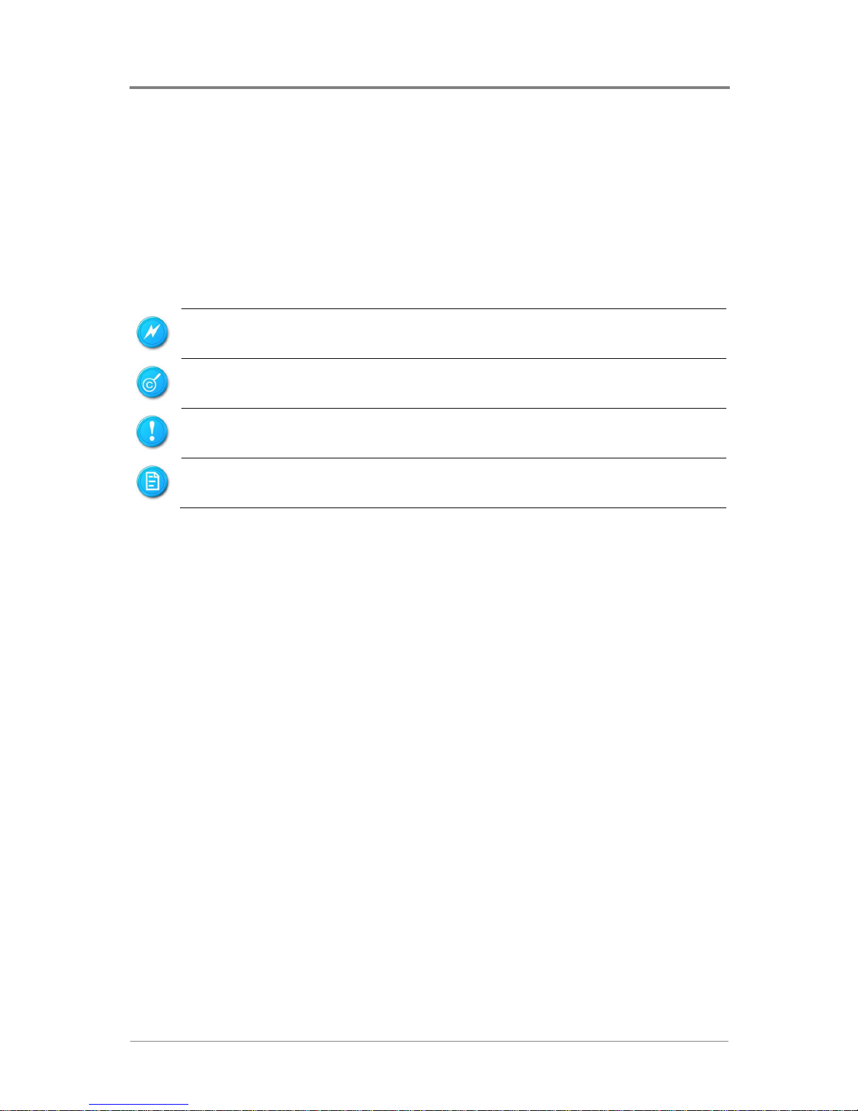
To make sure that you perform certain tasks properly, take note of the following symbols used
throughout this manual.
Warning:
Information to prevent injury to yourself when trying to complete a
task.
Caution:
Information to prevent damage to the components when trying to
complete a task.
Important:
Information that you must follow to complete a task.
Note:
Tips and information to aid in completing a task.
Page 10
About This Manual
2015-MNU-000006
ii
Safety Symbols
Before troubleshooting, you must be familiar with the safety information listed below. In order
to avoid any potential hazards, the following symbols may be placed on some components of
the server.
The shape and the color of symbols shown below are mainly for your reference. Please take
the actual shipment as standard.
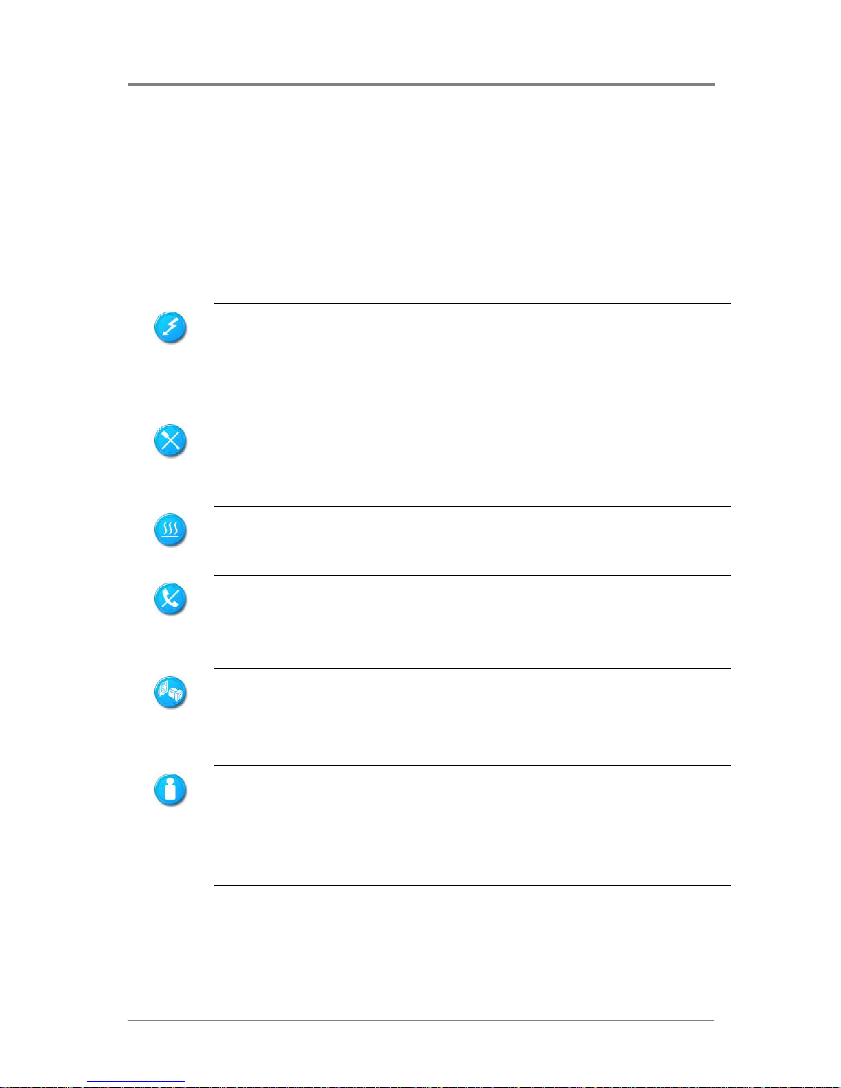
Indicates the potential hazard of energy circuits or electric shock. To reduce the
risk of injury from electric hazards, do not open this enclosure.
Warning: Any surface or area of the equipment marked with this symbol
indicates the presence of electric shock hazards. The enclosed area contains no
operator serviceable parts.
Indicates the potential hazard of electric shock. The enclosed area contains no
user of field serviceable parts. Do not open for any reason.
Warning: To reduce the risk of injury from electric shock hazards, do not open
this enclosure.
Indicates the presence of a hot surface or hot component.
Warning: To reduce the risk of injury from a hot component, allow the surface to
cool before touching it.
Any RJ45 receptacle marked with this symbol indicates a network interface
connection.
Warning: To reduce the risk of electric shock, fire, or damage to the equipment,
Do not plug telephone or telecommunications connectors into this receptacle.
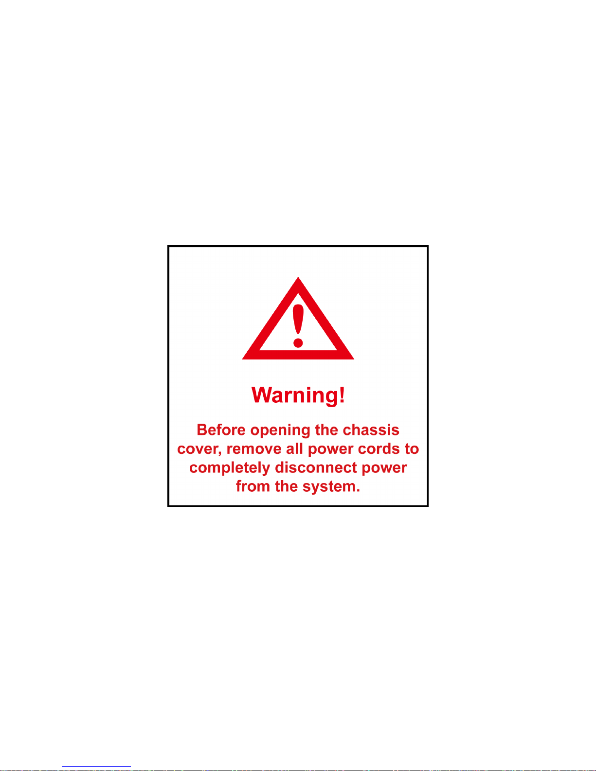
This symbol, on power supplies or systems, indicates that the equipment is
supplied by multiple sources of power.
Warning: To reduce the risk of injury from electric shock, remove all power
cords to completely disconnect power from the system.
Weight in kg
Weight in lb
This symbol indicates that the component exceeds the recommended weight for
one individual to handle safely.
Warning: To reduce the risk of personal injury or damage to the equipment,
observe local occupational health and safety requirements and guidelines for
manual material handling.
Page 11
About This Manual
2015-MNU-000006
iii
Safety Precautions
Observe the following safety precautions when you are connecting or disconnecting any
device.
•
Regarding the standards of workstation regulations, do not place the server in the visual
field of the user, because of the glossy front of the case.
•
The product is non-consumer product and for profession technical person used only.
Operation Safety
•
Any operation on this server must be conducted by certified or experienced engineers.
•
Before operating your server, carefully read all the manuals included with the server
package.
•
Before using the server, make sure that all cables are correctly connected and power
cords are not damaged. If any damage is detected, contact your dealer as soon as
possible.
•
To avoid short circuits, keep paper clips, screws, and staples away from connectors, slots,
sockets and circuitry.
•
Before opening the chassis panels, make sure all power cords are unplugged.
•
Avoid dust, humidity, and extreme temperatures, place the server on a stable surface.
•
If the power supply is broken, do not try to fix it by yourself. Contact an authorized dealer.
•
It is recommended that you wear gloves when assembling or disassembling the server to
protect from cuts and scrapes.
•
When the server is powered on, heat sinks and the surfaces of certain IC devices may be
hot. Do not touch them. Check whether the fans are functioning properly.
Electrical Safety
•
Before installing or removing signal cables, ensure that the power cords for the system
unit and all attached devices are unplugged.
•
To prevent electric shock hazard, disconnect the power cord from the electrical outlet
before relocating the system.
•
When adding or removing any additional devices to or from the system, ensure that the
power cords for those devices are unplugged before the signal cables are connected. If
possible, disconnect all power cords from the existing system before you add a device.
Page 12
About This Manual
2015-MNU-000006
iv
•
Use one hand, when possible, to connect or disconnect signal cables to prevent a
possible shock from touching two surfaces with different electrical potentials.
•
This product is equipped with a three-wire power cord and plug for user safety. Use the
power cord with a properly Grounded electrical outlet to avoid electric shock.
Motherboards, adapters, and disk drives are sensitive to static electricity discharge. These
devices are wrapped in antistatic bags to prevent this damage. Take the following
precautions:
•
If you have an antistatic wrist strap available, use it while handling the device.
•
Do not remove the device from the antistatic bag until you are ready to install the device in
the system unit.
•
With the device still in its antistatic bag, touch it to a metal frame of the system.
•
Grasp cards and boards by the edges. Hold drives by the frame. Avoid touching the solder
joints or pins.
•
If you need to lay the device down while it is out of the antistatic bag. Lay it on the
antistatic bag. Before picking it up again, touch the antistatic bag and the metal frame of
the system unit at the same time.
•
Handle the devices carefully to prevent permanent damage.
Battery Replacement Safety
This server is provided with an internal Lithium battery or battery pack. There is a danger of
explosion and risk of personal injury if the battery is incorrectly replaced or mistreated.
For more information about battery replacement or proper disposal, contact an authorized
reseller or your authorized service provider.
This server contains an internal Lithium Manganese Dioxide, or a Vanadium Pentoxide, or an
alkaline battery pack. There is risk of fire and burns if the battery pack is not handled properly.
To reduce the risk of personal injury:
•
Do not attempt to recharge the battery.
•
Do not expose to temperatures higher than 70°C.
•
Do not disassemble, crush, puncture, shorten external contacts, or dispose in fire or
water.
•
Replace only with the spare parts designated for this product.
Page 13

About This Manual
2015-MNU-000006
v
Batteries should not be littered along with the general household waste. Please use the public
collection system or return them to the supplier.
Laser Peripherals or Devices Safety
To avoid risk of radiation exposure and/or personal injury:
•
Do not open the enclosure of any laser peripheral or device.
•
Laser peripherals or devices are not user serviceable.
•
Return to manufacturer for servicing.
Intended Application Uses
This product was evaluated as Information Technology Equipment (ITE), which may be
installed in offices, schools, computer rooms, and similar commercial type locations. The
suitability of this product for other product categories and environments (such as medical,
industrial, residential, alarm systems, and test equipment), other than an ITE application, may
require further evaluation.
Site Selection
The system is designed to operate in a typical office environment. Choose a site that is:
•
Clean, dry, and free of airborne particles (other than normal room dust).
•
Well-ventilated and away from sources of heat including direct sunlight and radiators.
•
Away from sources of vibration or physical shock.
•
Isolated from strong electromagnetic fields produced by electrical devices.
•
In regions that are susceptible to electrical storms, we recommend you plug your system
into a surge suppresser and disconnect telecommunication lines to your modem during an
electrical storm.
•
Provided with a properly Grounded wall outlet.
•
Provided with sufficient space to access the power supply cord(s), because they serve as
the product's main power.
Page 14

About This Manual
2015-MNU-000006
vi
Tools Required
A cross screwdriver or a flat screwdriver is needed to install or remove the components in the
server.
Regulatory and Integration Information
Regulatory Compliance Identification Numbers
For the purpose of regulatory compliance certifications and identification, this motherboard is
assigned a serial number. This server serial number can be found on the product label, along
with the required approval markings and information. When requesting certification
information for this product, always refer to this serial number. This serial number should not
be confused with the marketing name or model number.
Product Regulatory Compliance
Worldwide Safety approvals can be supplied according to the requirements from Marketing or
Customer.
Product Safety Compliance
The motherboard complies with the following safety requirements:
Table i Product Safety Requirements
IEC 60950-1 Safety of Information Technology Equipment
EN 60950-1 Safety of Information Technology Equipment Including Electrical
Business Equipment, European Committee for Electrotechnical
Standardization (CENELEC)
UL 60950-1 Safety of Information Technology Equipment
UL 94 Tests for Flammability of Plastic Materials for Parts in Devices &
Appliances
GB4943 Safety of Information Technology Equipment
Product EMC Compliance
This product has been tested and verified to comply with the following electromagnetic
compatibility (EMC) regulations.
Communications Commission Notice
Part 15 of the Federal Communications Commission (FCC) Rules and Regulations has
established Radio Frequency (RF) emission limits to provide an interference-free radio
Page 15

About This Manual
2015-MNU-000006
vii
frequency spectrum. Many electronic devices, including computers, generate RF energy
incidental to their intended function and are, therefore, covered by these rules. These rules
place computers and related peripheral devices into two classes, A and B, depending upon
their intended installation. Class A devices are those that may reasonably be expected to be
installed in a business or commercial environment. Class B devices are those that may
reasonably be expected to be installed in a residential environment (for example, personal
computers). The FCC requires devices in both classes to bear a label indicating the
interference potential of the device as well as additional operating instructions for the user.
The rating label on the device shows which class (A or B) the equipment falls into. Class A
devices do not have an FCC logo or FCC ID on the label. Class B devices have an FCC logo
or FCC ID on the label. Once the class of the device is determined, refer to the following
corresponding statement.
Class A Equipment
This equipment has been tested and found to comply with the limits for a Class A digital
device, pursuant to Part 15 of the FCC Rules. These limits are designed to provide
reasonable protection against harmful interference when the equipment is operated in a
commercial environment. This equipment generates, uses, and can radiate radio frequency
energy and, if not installed and used in accordance with the instructions, may cause harmful
interference to radio communications. Operation of this equipment in a residential area is
likely to cause harmful interference, in which case the user will be required to correct the
interference at personal expense.
Declaration of Conformity for Products Marked with the FCC Logo—United States Only
This device complies with Part 15 of the FCC Rules Operation and is subject to the following
two conditions: (1) this device may not cause harmful interference, and (2) this device must
accept any interference received, including interference that may cause undesired operation.
For questions regarding your product, please contact the supplier.
To identify this product, refer to the Part, Series, or Model number found on the product.
European Union Notice
Products with the CE Marking comply with both the EMC Directive (89/336/EEC) and the
Low-Voltage Directive (73/23/EEC) issued by the Commission of the European Community.
Compliance with these directives implies conformity to the following European Norms (in
brackets are the equivalent international standards):
Page 16
About This Manual
2015-MNU-000006
viii
Table ii European Union EMC Requirements
EN55022 (CISPR 22) Electromagnetic Interference
EN55024 (IEC61000-4-2,3,4,5,6,8,11) Electromagnetic Immunity
EN61000-3-2 (IEC61000-3-2) Power Line Harmonics
EN61000-3-3 (IEC61000-3-3) Power Line Flicker
Canadian Notice (Avis Canadien)
Class A Equipment
Japanese Notice
Taiwanese Notice
Page 17

Audience Assumptions
Manual Organization
Product Features
Motherboard Layout
System LED Information
Chapter 1
Introduction
Page 18

Page 19

Introduction
2015-MNU-000006
1-1
1 Introduction
1.1 Audience Assumptions
This document is for the person who installs, administers, and troubleshoots motherboard.
Inventec Corporation assumes you are qualified in the servicing of computer equipment and
trained in recognizing hazards in products with hazardous energy levels.
1.2 Manual Organization
This manual introduces the motherboard along with the hardware information and how to
replace the hardware. This manual is generally organized as follows:
Table 1-1 Manual Introduction
Introduction
General motherboard introduction and LED information.
Hardware Operation
The operation of the components on the motherboard, such as
system battery, processor, system memory, and so forth.
Connectors and
Jumpers
Necessary information such as the locations and functions of
connectors and jumpers on the motherboard.
Appendix
China RoHS Regulations information.
Page 20

Hardware Operations
2015-MNU-000006
1-2
1.3 Product Features
This chapter provides the detailed features for processor, chipset, system memory, onboard
storage, NIC, VGA, I/O and PCI slot with pictures for your reference.
Figure 1-1 Motherboard Overview
This motherboard dimension is designed for 20.2” x 6.6”. This motherboard supports Intel®
Xeon™ E5-2600 V3 product family, Haswell-EP processors, based on Intel® C612 Wellsburg
platform chipset. The following highlights are the main features of the motherboard.
Table 1-2 Product Features
Processor
2x Intel® XeonTM E5-2600 V3 product family
Designed up to 145W (restricted below 120W in
consideration of thermal factors)
Intel Socket R3 (LGA2011-3)
Hyper-Threading
Turbo boost
EVRD 12.5
PCI-E Gen3
QPI 8.0GT/s, 9.6GT/s
Chipset
Intel C612 Wellsburg PCH
System Memory
16x DDR4 1333/1600/1866/2133 MT/s ECC RDIMMs
4x DDR4 channel per CPU
RDIMMs and LRDIMMs
1.2V DDR4 standard I/O voltage
Up to 8 ranks supported per channel, 1, 2, or 4 ranks
Page 21

Introduction
2015-MNU-000006
1-3
per DIMM
Max memory capacity up to 512GB per processor
NIC
Intel® NH i350/X540/82599 OCP NIC
i350 supports dual ports 1G Base-T connection
X540 supports dual ports 10G Base-T connection
82599 supports dual ports SFP+ connection
Server Management
ASPEED AST2400, IPMI2.0 Complaint
1 management RJ45 port with 10/100Mbps
Onboard Storage Ports
10 SATA III connectors
2x SATA 6Gb/s ports based on Wellsburg PCH
8x SATA 6Gb/s ports based on 2 HDminiSAS ports
Intel RSTe RAID 0/1/10/5
AHCI mode
VGA
ASPEED AST2400 embedded
16MB with AST2300 (DDR3)
Rear IO Ports
2x 1Gb/10Gb RJ45 Ports or 2x SFP+ ports on OCP
NIC
2x USB 3.0 ports
1x VGA connector
1x ID Button/LED
1 RJ45 management port
Onboard Slots
1 PCI-E x8 + x8 G3 slot
2 PCI-E x8 Mezzanine slot
Page 22

Hardware Operations
2015-MNU-000006
1-4
1.4 Motherboard Layout
The layout of the motherboard is shown below. Each connector and major component is
identified by number.
Figure 1-2 Connector and Component Location of Motherboard
Page 23

Introduction
2015-MNU-000006
1-5
1 Power Button/LED (SW1)
2 VGA Connector (J39)
3 IPMB Connector (J62)
4 Host SMBus Connector (J52)
5 ME Upgrade Jumper (J63)
6 ID Button/LED (SW2)
7 BMC Reset Button (SW3)
8 Management Port (J50)
9 CPLD JTAG Connector (J60)
10 1Gbe NIC 1 (on OCP 1G/10G Base-T NIC)
11 1Gbe NIC 2 (on OCP 1G/10G Base-T NIC)
12 UART Connector (J29)
13 System Health LED (CR1)
14 USB Port (J33)
15 QPI Slow Jumper (J58)
16 PCI-E x16 Slot (J37)
17 Mezz Slot 1 (J26)
18
Mezz Slot 2 (J57)
19 SATA SGPIO Connector (J41)
20 BMC Debug Connector (J44)
21 Power Debug Header (J70)
22 TPM Connector (J2)
23 SGPIO Connector (J71)
24 BP LED Connector (J72)
25 DIMM Slots for Processor 0 (J11, J12, J13, J14)
26 Processor 0 (U25)
27 XDP Connector (J46)
28 Processor 1 (U26)
29 DIMM Slots for Processor 1 (J15, J16, J17, J18)
30 PCI-E Mini-SAS Connector (J3)
31 Middle Plane Connector (J76, J77)
32 BP Mini-SAS Connector (J24)
33 DIMM Slots for Processor 1 (J19, J20, J21, J22)
34 Battery (BH1)
35 DIMM Slots for Processor 0 (J7, J8, J9, J10)
36 BP Power Connector (J64)
Page 24

Hardware Operations
2015-MNU-000006
1-6
37 Power FW Flash Header (J125)
38 Clear Password Jumper (J51)
39 Clear CMOS Jumper (J59)
40 Internal USB Connector (J81)
41 PCH SATA Connector 0 (J32)
42 BIOS Recovery Jumper (J27)
43 Intruder Header (J53)
44 Repeater I2C Connector (J79)
45 SATA DOM Power Connector (J6)
46 PCH SATA Connector 1 (J34)
47 PCH SATA Connector 2~5 (J42)
48 NMI Jumper (J75)
49 ME Recovery Jumper (J49)
50 PCH SSATA Connector 0~3 (J1)
1.5 Back Panel LED Information
The back panel LED information displays details regarding the NIC LEDs, the management
port LED and the ID LED. The NIC port and management port contains two LEDs that show
the status of network activity, link or speed.
Figure 1-3 Back Panel LEDs
1 System Health LED
2 1Gbe NIC 2 Link/Activity LED (on OCP 1G/10G Base-T NIC)
3 1Gbe NIC 2 Speed LED (on OCP 1G/10G Base-T NIC)
4 1Gbe NIC 1 Link/Activity LED (on OCP 1G/10G Base-T NIC)
5 1Gbe NIC 1 Speed LED (on OCP 1G/10G Base-T NIC)
6 Management Port Link/Activity LED
Page 25

Introduction
2015-MNU-000006
1-7
7 Management Port Speed LED
8 BMC Reset Button
9 ID LED
10 Power LED
11 10Gbe NIC 2 Speed LED (on OCP SFP+ NIC)
12 10Gbe NIC 2 Link/Activity LED (on OCP SFP+ NIC)
13 10Gbe NIC 1 Link/Activity LED (on OCP SFP+ NIC)
14 10Gbe NIC 1 Speed LED (on OCP SFP+ NIC)
The detailed LED information is shown below:
Table 1-3 LED Information of NIC Port
Type of
LED
Link/Activity
Speed
Color Status
NIC Ports
Link/Activity Green
On LAN link/No access
Blinking LAN access
Off No connection
10GbE Speed
Green
On Linked to the network at 10Gbps
Amber
On Linked to the network at other speed
1GbE Speed
Green
On Linked to the network at 1Gbps
Amber
On Linked to the network at other speed
Table 1-4 LED Information of Management Port
Type of LED
Speed/Link
Status
Management
Port
Green Speed
LED on Left
On Linked to the network at 100Mbps
Off Linked to the network at 10Mbps
Green Link LED
on Right
On LAN Link/No Access
Blinking LAN Link/Access
Off No Connection
Table 1-5 ID LED Information
Type of
LED
Color Status
ID Blue On
Turned on through IPMI command or by
pressing down the button
Page 26

Hardware Operations
2015-MNU-000006
1-8
Off
Turned off through IPMI command or by
pressing down the button
Page 27

Before You Start
Screw Holes
System Battery
Processor
System Memory
Chapter 2
Hardware Operations
Page 28

Page 29

Page 30

Page 31

Hardware Operations
2015-MNU-000006
2-1
2 Hardware Operation
This chapter provides the detailed information and replacement steps for motherboard,
including system battery, processor, system memory, and system configuration jumper.
2.1 Before You Start
Take note of the following precautions before you remove and install any components on the
motherboard.
Reminder
Before you remove or install the components on motherboard please follow the steps below:
Step 1:
Make sure the server is not turned on or connected to the AC power.
Step 2: Remove the chassis cover.
Moving the Power On/Off switch to the Off position does not completely remove
system power. Some portions of the power supply and some internal circuitry remain
active. Disconnect all power cords from the server to remove all power from the
system.
•
The components shown in this chapter are mainly for your reference. Please take
the actual shipment as standard.
•
All descriptions in this chapter are based on one motherboard except special
statement.
To reduce the risk of injury from electric shock, remove the power cord to completely
disconnect power from the system.
Page 32

Hardware Operations
2015-MNU-000006
2-2
2.2 Screw Hole
The motherboard is designed with totally eight screw holes as the picture shows.
Figure 2-1 Screws Placement
Screw Hole
Do not overly tighten the screws. Doing so may damage the motherboard.
Page 33

Hardware Operations
2015-MNU-000006
2-3
2.3 System Battery
The location of system battery is shown below:
Figure 2-2 System Battery Location
2.3.1 To remove the system battery
Pull the battery retaining clip away from the system battery.
Lift the system battery on the lever side and pull it out of the holder.
Figure 2-3 Pulling the System Battery out of the Holder
Do not bend the retaining clip during system battery replacement. For proper
operation, the clip must maintain a position of contact with the system battery.
2.3.2 To install the system battery
Put the system battery into the holder in the direction as shown below.
Figure 2-4 Putting the System Battery into the Holder
Page 34

Hardware Operations
2015-MNU-000006
2-4
2.4 Processor
This motherboard supports dual Intel® Xeon™ E5-2600 series processors.
The location of processors on the motherboard is shown below:
Figure 2-5 Location of Processors
Processor 0
Processor 1
2.4.1 To remove the heat sink
Loosen the securing screws.
Lift the heat sink up from the installed processor.
Figure 2-6 Removing the Heat Sink
2.4.2 To install the heat sink
Reverse the steps above to install the heat sink.
Before you put the heat sink on top of the installed processor, please do not forget
to check if the grease is complete on bottom of the heat sink.
The heat sink used in the figure below is just for your reference. Please choose an
appropriate heat sink depending on the whole system requirement.
Page 35

Hardware Operations
2015-MNU-000006
2-5
2.4.3 To remove the processor
Unlock the load lever 1 and lift it up.
Unlock the load lever 2 and lift it up.
Open the load plate.
Figure 2-7 Opening the Load Plate
Lift the processor out of the socket.
Figure 2-8 Lifting the Processor out of the Socket
Close the load plate.
Lock the load lever 2.
Lock the load lever 1.
Page 36

Hardware Operations
2015-MNU-000006
2-6
Figure 2-9 Closing the Load Plate
Put the PnP Cap on the load plate.
Figure 2-10 Installing the PnP Cap
2.4.4 To install the processor
Reverse the steps above to install the processor. However, when inserting the processor into
the socket, make sure that the golden corner on the processor is pointed toward the socket as
picture shows:
Figure 2-11 Pointing the Golden Corner toward the Socket
Page 37

Hardware Operations
2015-MNU-000006
2-7
•
When the processor is in place, press it firmly on the socket while you push
down the socket lever to secure the processor. The lever clicks on the socket
indicating that it is locked.
•
The processor fits only in one orientation. Do not force the processor into the
socket to avoid bending the pins and damaging the processor. If the processor
does not fit completely, check its orientation or check for bent pins.
2.5 System Memory
This motherboard supports 16 DDR4 1333/1600/1866/2133 MT/s DIMMs, RDIMMs, and
LRDIMMs. Each processor supports four DDR4 channels.
The location of DIMM sockets on the motherboard is shown below:
Figure 2-12 Location of System Memories
There are 16 DIMMs on the motherboard to support the processor. The DIMM sequence of
the DIMM sockets is respectively shown below.
Page 38

Hardware Operations
2015-MNU-000006
2-8
Figure 2-13 DIMM Socket Location
Page 39

Hardware Operations
2015-MNU-000006
2-9
2.5.1 To remove a DIMM
Unlock a DIMM socket by pressing the retaining clips outward. This action releases the
module and partially lifts it out of the socket.
Lift out the DIMM.
Page 40

Hardware Operations
2015-MNU-000006
2-10
Figure 2-14 Lifting the DIMM out of the Socket
2.5.2 To install a DIMM
Unlock a DIMM socket by pressing the retaining clips outward.
Figure 2-15 Pressing the Retaining Clips Outward
Align the notch on the DIMM to the break on the socket. Carefully insert the DIMM into the
socket until the retaining clips snap back in place.
Figure 2-16 Inserting the DIMM into the Socket
DIMMs fit in only one direction. DO NOT force a DIMM into the socket to avoid
damaging the DIMM.
Page 41

Chapter 3
Connectors and Jumpers
PCH SSATA /PCH SATA Connector
PCH SATA Connector
SATA SGPIO Connector
MINI-SAS Connector
Middle Plane Connector
Jumper Settings
Page 42

Page 43

Connectors and Jumpers
2015-MNU-000006
3-1
3 Connectors and Jumpers
The locations of all the connectors described in this chapter are shown in “1.4 Motherboard
Layout”.
“Key” stands for foolproof feature; “NC” stands for unused.
3.1 PCH SSATA (J1) / PCH SATA Connector (J42)
Figure 3-1 PCH SSATA / PCH SATA Connector
Table 3-1 Pin Definition of PCH SSATA / PCH SATA Connector (J1)
Signal Name Pin
Pin Signal Name
PCH_SSATA_TX_0_DP C7 A7 PCH_SSATA_RX_0_DP
PCH_SSATA_TX_0_DN C8 A8 PCH_SSATA_RX_0_DN
PCH_SSATA_TX_1_DP D7 B7 PCH_SSATA_RX_1_DP
PCH_SSATA_TX_1_DN D8 B8 PCH_SSATA_RX_1_DN
PCH_SSATA_TX_3_DP C4 A4 PCH_SSATA_RX_3_DP
PCH_SSATA_TX_3_DN C5 A5 PCH_SSATA_RX_3_DN
PCH_SSATA_TX_2_DP D4 B4 PCH_SSATA_RX_2_DP
PCH_SSATA_TX_2_DN D5 B5 PCH_SSATA_RX_2_DN
DC_PCH_SSATA_SIDEBAND6 D2 D1 DC_PCH_SSATA_SIDEBAND5
Ground C2 C1 SGPIO_SSATA_DATAOUT0_R
SGPIO_SSATA_LOAD_R B2 B1 Ground
SGPIO_SSATA_CLOCK_R A2 A1 DC_PCH_SSATA_SIDEBAND7
Ground
B9 D9
Ground
Ground
B6 D6
Ground
Ground
B3 D3
Ground
Ground
A3 C3
Ground
Ground
A6 C6
Ground
Ground
A9 C9
Ground
Page 44

Connectors and Jumpers
2015-MNU-000006
3-2
Table 3-2 Pin Definition of PCH SATA Connector (J42)
Signal Name Pin
Pin Signal Name
PCH_SATA_TX_4_DP C7 A7 PCH_SATA_RX_4_DP
PCH_SATA_TX_4_DN C8 A8 PCH_SATA_RX_4_DN
PCH_SATA_TX_2_DP D7 B7 PCH_SATA_RX_2_DP
PCH_SATA_TX_2_DN D8 B8 PCH_SATA_RX_2_DN
PCH_SATA_TX_5_DP C4 A4 PCH_SATA_RX_5_DP
PCH_SATA_TX_5_DN C5 A5 PCH_SATA_RX_5_DN
PCH_SATA_TX_3_DP D4 B4 PCH_SATA_RX_3_DP
PCH_SATA_TX_3_DN D5 B5 PCH_SATA_RX_3_DN
DC_PCH_SATA_SIDEBAND6 D2 D1 DC_PCH_SATA_SIDEBAND5
Ground C2 C1 SGPIO_SATA_DATAOUT0
SGPIO_SATA_LOAD B2 B1 Ground
SGPIO_SATA_CLOCK A2 A1 DC_PCH_SATA_SIDEBAND7
Ground
B9 D9
Ground
Ground
B6 D6
Ground
Ground
B3 D3
Ground
Ground
A3 C3
Ground
Ground
A6 C6
Ground
Ground
A9 C9
Ground
3.2 PCH SATA Connectors (J32, J34)
Figure 3-2 PCH SATA Connectors
Table 3-3 Pin Definition of PCH SATA Connector (J32)
Signal Name Pin
7 Ground
6 PCH_SATA_RX_0_DP
5 PCH_SATA_RX_0_DN
4 Ground
Page 45

Connectors and Jumpers
2015-MNU-000006
3-3
Signal Name Pin
3 PCH_SATA_TX_0_DN
2 PCH_SATA_TX_0_DP
1 Ground
8 P5V_SATA_DOM_9
9 Ground
Table 3-4 Pin Definition of PCH SATA Connector (J34)
Signal Name Pin
7 Ground
6 PCH_SATA_RX_1_DP
5 PCH_SATA_RX_1_DN
4 Ground
3 PCH_SATA_TX_1_DN
2 PCH_SATA_TX_1_DP
1 Ground
8
Ground
9
Ground
3.3 SATA SGPIO Connector (J41)
Figure 3-3 SATA SGPIO Connector
Table 3-5 Pin Definition of SATA SGPIO Connector (J41)
Signal Name Pin
1 SGPIO_SATA_LOAD
2 SGPIO_SATA_DATAOUT0
3 Ground
4 SGPIO_SATA_CLOCK
5 DC_SGPIO_P5
Page 46

Connectors and Jumpers
2015-MNU-000006
3-4
3.4 MINI-SAS Connectors (J3, J24)
Figure 3-4 MINI-SAS Connectors
Table 3-6 Pin Definition of MINI-SAS Connector (J3)
Signal Name Pin
Pin Signal Name
PE3_CPU1_TX_DP<3> C7 A7 PE3_CPU1_RX_DP<3>
PE3_CPU1_TX_DN<3> C8 A8 PE3_CPU1_RX_DN<3>
PE3_CPU1_TX_DP<2> D7 B7 PE3_CPU1_RX_DP<2>
PE3_CPU1_TX_DN<2> D8 B8 PE3_CPU1_RX_DN<2>
PE3_CPU1_TX_DP<1> C4 A4 PE3_CPU1_RX_DP<1>
PE3_CPU1_TX_DN<1> C5 A5 PE3_CPU1_RX_DN<1>
PE3_CPU1_TX_DP<0> D4 B4 PE3_CPU1_RX_DP<0>
PE3_CPU1_TX_DN<0> D5 B5 PE3_CPU1_RX_DN<0>
I2C_BMC_SSD_1_SCL D2 D1 I2C_BMC_SSD_1_SDA
I2C_PEHP_CPU1_SCL_P3V3_1A C2 C1 I2C_PEHP_CPU1_SDA_P3V3_1A
Ground B2 B1 RST_CPU1_PE_SSD_N
CLK_100M_CPU1_PE3_SSD1_DN A2 A1 CLK_100M_CPU1_PE3_SSD1_DP
Ground
B9 D9
Ground
Ground
B6 D6
Ground
Ground
B3 D3
Ground
Ground
A3 C3
Ground
Ground
A6 C6
Ground
Ground
A9 C9
Ground
PE3_CPU1_TX_DP<7>
C16 A16
PE3_CPU1_RX_DP<7>
PE3_CPU1_TX_DN<7>
C17 A17
PE3_CPU1_RX_DN<7>
PE3_CPU1_TX_DP<6>
D16 B16
PE3_CPU1_RX_DP<6>
PE3_CPU1_TX_DN<6>
D17 B17
PE3_CPU1_RX_DN<6>
PE3_CPU1_TX_DP<5>
C13 A13
PE3_CPU1_RX_DP<5>
PE3_CPU1_TX_DN<5>
C14 A14
PE3_CPU1_RX_DN<5>
PE3_CPU1_TX_DP<4>
D13 B13
PE3_CPU1_RX_DP<4>
PE3_CPU1_TX_DN<4>
D14 B14
PE3_CPU1_RX_DN<4>
I2C_BMC_SSD_2_SCL
D11 D10
I2C_BMC_SSD_2_SDA
Page 47

Connectors and Jumpers
2015-MNU-000006
3-5
Signal Name Pin
Pin Signal Name
I2C_CPU1_SSD_2_SCL
C11 C10
I2C_CPU1_SSD_2_SDA
Ground
B11 B10
RST_CPU1_PE_SSD_N
CLK_100M_CPU1_PE3_SSD2_DN
A11 A10
CLK_100M_CPU1_PE3_SSD2_DN
Ground
C15 A12
Ground
Ground
D15 B12
Ground
Ground
A18 C12
Ground
Ground
B18 D12
Ground
Ground
C18 A15
Ground
Ground
D18 B15
Ground
Table 3-7 Pin Definition of MINI-SAS Connector (J24)
Signal Name Pin
Pin Signal Name
SATA_TX7_BP_DP C7 A7 SATA_RX7_BP_DP
SATA_TX7_BP_DN C8 A8 SATA_RX7_BP_DN
SATA_TX5_BP_DP D7 B7 SATA_RX5_BP_DP
SATA_TX5_BP_DN D8 B8 SATA_RX5_BP_DN
SATA_TX6_BP_DP C4 A4 SATA_RX6_BP_DP
SATA_TX6_BP_DN C5 A5 SATA_RX6_BP_DN
SATA_TX4_BP_DP D4 B4 SATA_RX4_BP_DP
SATA_TX4_BP_DN D5 B5 SATA_RX4_BP_DN
D2 D1
C2 C1 SATA_SIO_DOUT2
SATA_SIO_LOAD2 B2 B1 Ground
SATA_SIO_CLK2 A2 A1
Ground
B9 D9
Ground
Ground
B6 D6
Ground
Ground
B3 D3
Ground
Ground
A3 C3
Ground
Ground
A6 C6
Ground
Ground
A9 C9
Ground
SATA_TX3_BP_DP
C16 A16
SATA_RX3_BP_DP
SATA_TX3_BP_DN
C17 A17
SATA_RX3_BP_DN
SATA_TX1_BP_DP
D16 B16
SATA_RX1_BP_DP
SATA_TX1_BP_DN
D17 B17
SATA_RX1_BP_DN
SATA_TX2_BP_DP
C13 A13
SATA_RX2_BP_DP
SATA_TX2_BP_DN
C14 A14
SATA_RX2_BP_DN
Page 48

Connectors and Jumpers
2015-MNU-000006
3-6
Signal Name Pin
Pin Signal Name
SATA_TX0_BP_DP
D13 B13
SATA_RX0_BP_DP
SATA_TX0_BP_DN
D14 B14
SATA_RX0_BP_DN
D11 D10
C11 C10
SATA_SIO_DOUT1
SATA_SIO_LOAD1
B11 B10
Ground
SATA_SIO_CLK1
A11 A10
Ground
C15 A12
Ground
Ground
D15 B12
Ground
Ground
A18 C12
Ground
Ground
B18 D12
Ground
Ground
C18 A15
Ground
Ground
D18 B15
Ground
3.5 Middle Plane Connectors (J76, J77)
Figure 3-5 Middle Plane Connectors
Table 3-8 Pin Definition of Middle Plane Connector (J76)
Signal Name Pin
Pin Signal Name
Ground 1 2 Ground
PE3_CPU1_3_RX_DP<7> 3 4 PE3_CPU1_3_TX_DP<7>
PE3_CPU1_3_RX_DN<7> 5 6 PE3_CPU1_3_TX_DN<7>
Ground 7 8 Ground
Ground 9 10 Ground
PE3_CPU1_3_RX_DP<6> 11 12 PE3_CPU1_3_TX_DP<6>
PE3_CPU1_3_RX_DN<6> 13 14 PE3_CPU1_3_TX_DN<6>
Ground 15 16 Ground
Ground 17 18 Ground
PE3_CPU1_3_RX_DP<5> 19 20 PE3_CPU1_3_TX_DP<5>
PE3_CPU1_3_RX_DN<5> 21 22 PE3_CPU1_3_TX_DN<5>
Ground 23 24 Ground
Page 49

Connectors and Jumpers
2015-MNU-000006
3-7
Signal Name Pin
Pin Signal Name
Ground 25 26 Ground
PE3_CPU1_3_RX_DP<4> 27 28 PE3_CPU1_3_TX_DP<4>
PE3_CPU1_3_RX_DN<4> 29 30 PE3_CPU1_3_TX_DN<4>
Ground 31 32 Ground
Ground 33 34 Ground
PE3_CPU1_3_RX_DP<3> 35 36 PE3_CPU1_3_TX_DP<3>
PE3_CPU1_3_RX_DN<3> 37 38 PE3_CPU1_3_TX_DN<3>
Ground 39 40 Ground
Ground 41 42 Ground
PE3_CPU1_3_RX_DP<2> 43 44 PE3_CPU1_3_TX_DP<2>
PE3_CPU1_3_RX_DN<2> 45 46 PE3_CPU1_3_TX_DN<2>
Ground 47 48 Ground
Ground 49 50 Ground
PE3_CPU1_3_RX_DP<1> 51 52 PE3_CPU1_3_TX_DP<1>
PE3_CPU1_3_RX_DN<1> 53 54 PE3_CPU1_3_TX_DN<1>
Ground 55 56 Ground
Ground 57 58 Ground
PE3_CPU1_3_RX_DP<0> 59 60 PE3_CPU1_3_TX_DP<0>
PE3_CPU1_3_RX_DN<0> 61 62 PE3_CPU1_3_TX_DN<0>
Ground 63 64 Ground
Ground 65 66 Ground
I2C_BMC_SSD_FG_SCL 67 68 I2C_BMC_SSD_FG1_SCL
I2C_BMC_SSD_FG_SDA 69 70 I2C_BMC_SSD_FG1_SDA
Ground 71 72 CPLD_RSVD2
CLK_100M_PE_FINGER1_DP 73 74 CPLD_RSVD1
CLK_100M_PE_FINGER1_DN 75 76 Ground
RST_PCIE_FINGER 77 78 SATA_SIO_CLK2
IRQ_LVC3_WAKE_N 79 80 SATA_SIO_DOUT2
PSU_PGD_PS 81 82 SATA_SIO_LOAD2
BTN_UID_N 83 84 Ground
PAL_BMC_UID_LED_FP_N 85 86 SATA_SIO_LOAD1
FM_HLTH_RED_LED_N 87 88 SATA_SIO_DOUT1
FM_HLTH_GRN_LED_N 89 90 SATA_SIO_CLK1
CTNR_PS_ON_N 91 92 Ground
FCB_REQ_FET_N 93 94 I2C_FCB_SDA_BUF
BTN_FP_PWR_N 95 96 I2C_FCB_SCL_BUF
Page 50

Connectors and Jumpers
2015-MNU-000006
3-8
Signal Name Pin
Pin Signal Name
ACK_N 97 98 MLB_ID
Ground 99 100 EN_P2V5
I2C_G3_SDA_SLOT 101 102 RST_BMC_N_CM4
I2C_G3_SCL_SLOT 103 104 R2100
SGPIO_GSX_CLK_PLD 105 106 I2C_PEHP_CPU1_SCL_P3V3_3A
SGPIO_GSX_DOUT_PLD 107 108 I2C_PEHP_CPU1_SDA_P3V3_3A
SGPIO_GSX_LOAD_PLD 109 110 BUF_PGM_OUT02_R_N
MLB_HOT_N 111 112 Ground
SGPIO_GSX_DIN_PLD 113 114 Ground
CLK_100M_PE_FINGER_DP 115 116 I2C_G8_SCL_MAX24101
CLK_100M_PE_FINGER_DN 117 118 I2C_G8_SDA_MAX24101
Ground 119 120 Ground
Table 3-9 Pin Definition of Middle Plane Connector (J77)
Signal Name Pin
Pin Signal Name
Ground 1 2 Ground
SATA_RX7_BP_REP_C_DN 3 4 SATA_TX7_BP_DN
SATA_RX7_BP_REP_C_DP 5 6 SATA_TX7_BP_DP
Ground 7 8 Ground
Ground 9 10 Ground
SATA_RX6_BP_REP_C_DN 11 12 SATA_TX6_BP_DN
SATA_RX6_BP_REP_C_DP 13 14 SATA_TX6_BP_DP
Ground 15 16 Ground
Ground 17 18 Ground
SATA_RX5_BP_REP_C_DN 19 20 SATA_TX5_BP_DN
SATA_RX5_BP_REP_C_DP 21 22 SATA_TX5_BP_DP
Ground 23 24 Ground
Ground 25 26 Ground
SATA_RX4_BP_REP_C_DN 27 28 SATA_TX4_BP_DN
SATA_RX4_BP_REP_C_DP 29 30 SATA_TX4_BP_DP
Ground 31 32 Ground
Ground 33 34 Ground
SATA_RX3_BP_REP_C_DN 35 36 SATA_TX3_BP_DN
SATA_RX3_BP_REP_C_DP 37 38 SATA_TX3_BP_DP
Ground 39 40 Ground
Page 51

Connectors and Jumpers
2015-MNU-000006
3-9
Signal Name Pin
Pin Signal Name
Ground 41 42 Ground
SATA_RX2_BP_REP_C_DN 43 44 SATA_TX2_BP_DN
SATA_RX2_BP_REP_C_DP 45 46 SATA_TX2_BP_DP
Ground 47 48 Ground
Ground 49 50 Ground
SATA_RX1_BP_REP_C_DN 51 52 SATA_TX1_BP_DN
SATA_RX1_BP_REP_C_DP 53 54 SATA_TX1_BP_DP
Ground 55 56 Ground
Ground 57 58 Ground
SATA_RX0_BP_REP_C_DN 59 60 SATA_TX0_BP_DN
SATA_RX0_BP_REP_C_DP 61 62 SATA_TX0_BP_DP
Ground 63 64 Ground
Ground 65 66 Ground
P12V_STBY_MLB 67 68 P12V_STBY_MLB
P12V_STBY_MLB 69 70 P12V_STBY_MLB
P12V_STBY_MLB 71 72 P12V_STBY_MLB
P12V_1 73 74 P12V_1
P12V_1 75 76 P12V_1
P12V_1 77 78 P12V_1
P12V_1 79 80 P12V_1
P12V_1 81 82 P12V_1
P12V_1 83 84 P12V_1
P12V_1 85 86 P12V_1
P12V_1 87 88 P12V_1
P12V_1 89 90 P12V_1
P12V_1 91 92 P12V_1
P12V_1 93 94 P12V_1
P12V_1 95 96 P12V_1
P12V_1 97 98 P12V_1
P12V_1 99 100 P12V_1
P12V_1 101 102 P12V_1
P12V_1 103 104 P12V_1
Ground 105 106 Ground
Ground 107 108 Ground
Ground 109 110 Ground
Ground 111 112 Ground
Page 52

Connectors and Jumpers
2015-MNU-000006
3-10
Signal Name Pin
Pin Signal Name
Ground 113 114 Ground
Ground 115 116 Ground
Ground 117 118 Ground
Ground 119 120 Ground
3.6 Jumper settings
3.6.1 Clear Password Jumper (J51)
The function of Clear Password jumper on the motherboard is shown below:
Figure 3-6 Clear Password Jumper
Table 3-10 Clear Password Jumper Function
Function
Clear Password
3.6.2 Clear CMOS Jumper (J59)
The function of Clear CMOS jumper on the motherboard is shown below:
Figure 3-7 Clear CMOS Jumper
Table 3-11 Clear CMOS Jumper Function
Function
Clear CMOS
Page 53

Connectors and Jumpers
2015-MNU-000006
3-
11
3.6.3 BIOS Recovery Jumper (J27)
The function of BIOS Recovery jumper on the motherboard is shown below:
Figure 3-8 BIOS Recovery Jumper
Table 3-12 BIOS Recovery Jumper Function
Function
BIOS Recovery
3.6.4 ME Firmware Recovery Jumper Setting (J49)
The function of ME Firmware Recovery jumper on the motherboard is shown below:
Figure 3-9 ME Firmware Recovery Jumper
Table 3-13 ME Firmware Recovery Jumper Function
Function
ME Firmware Recovery
3.6.5 Intruder Header (J53)
The function of Intruder Header on the motherboard is shown below:
Figure 3-10 Intruder Header
Table 3-14
Intruder Header Function
Page 54

Connectors and Jumpers
2015-MNU-000006
3-12
Function
Intruder
3.6.6 QPI Slow Jumper (J58)
The function of QPI Slow jumper on the motherboard is shown below:
Figure 3-11 QPI Slow Jumper
Table 3-15 QPI Slow Jumper Function
Function
QPI Slow Jumper
3.6.7 NMI Jumper (J75)
The function of the NMI jumper on the motherboard is shown as below:
Figure 3-12 NMI Jumper
Table 3-16 NMI Jumper Function
Function
NMI Jumper
Page 55

Connectors and Jumpers
2015-MNU-000006
3-13
3.6.8 Force ME Upgrade Jumper (J63)
The function of the Force ME Upgrade jumper on the motherboard is shown below:
Figure 3-13 Force ME Upgrade Jumper
Table 3-17 Force ME Upgrade Jumper Function
Function
Force ME Upgrade
Jumper
Page 56

Page 57

Appendix
China RoHS Regulations
Page 58

Page 59

Page 60

Page 61

Appendix
2015-MNU-000006
I
Appendix China RoHS Regulations
Appendix Figure I China RoHS Regulations
 Loading...