


User’s Manual
XC-RF850 Reader
Invengo Information Technology Co., Ltd.

Thank you for using Invengo’s RFID products!
We are glad that you’ve chosen XC-RF850 UHF RFID reader.
We hope our product will make your daily tasks at work easier!
Foreword
This user manual is intended for using with XC-RF850 FCJ/FCW/FLJ/FLW
This manual provides information on product application, maintenance, repair and other
features for users and maintenance staff of the products.
The version of this manual is V1.0, with revision record as follows:
19
th
Jan 2015 Initial draft V1.0
or are Invengo’s trademarks.
All introduction and explanation on the product features, as well as the functions and other
related information, written in this manual, are the latest and accurate as at time of print.
The company reserves all rights to make any correction or amendment to this manual without
prior notice, and shall bear no responsibility for these actions.

Main content
Product Overview
Reader Installation and Commissioning
DEMO User Guide
Routine maintenance and service
Transportation and storage
Packaging and Inspection
After-sale service
Safety Instructions
Warning sign
Improper handling may cause damage to health.
Improper handling may result in equipment damage.
Notication sign
If ignored, it may result in unsuccessful operation.
If ignored, it may result in undesired effect.

Content
1 Product Overview ......................................................................... 1
1.1 Brief introduction ........................................................................................... 1
1.2 Main usage and application range ............................................................... 1
1.3 Product certicate.......................................................................................... 2
1.4 Applicable regions and frequency bands .................................................... 3
1.5 Operation condition ....................................................................................... 3
1.6 Safety and protective measures ................................................................... 3
1.7 Main functions ................................................................................................ 4
1.8 Technical parameters .................................................................................... 4
1.9 Dimensions ..................................................................................................... 5
1.10 Weight ........................................................................................................... 5
2 Reader installation and commissioning ....................................6
2.1 Unboxing instruction ..................................................................................... 6
2.2 Installation requirement ................................................................................ 6
2.3 Panel description ........................................................................................... 7
2.3.1 I/O and communication patch panel ..................................................................... 7
2.3.2 RF connector panel ............................................................................................ 10
2.3.3 LED display panel .............................................................................................. 11
2.4 Commissioning preparation ........................................................................11
2.4.1 Personal computer Require ................................................................................. 11
2.4.2 Reader interface software ................................................................................... 12
2.4.3 External antenna ................................................................................................. 12

2.5 Safety during installation ............................................................................ 14
2.5.1 External RF cable ................................................................................................ 14
2.5.2 Power and communication interface cable ......................................................... 15
2.5.3 I/O control port cable .......................................................................................... 17
2.6 Equipment installation ................................................................................. 19
2.7 Common scenario during commissioning ............................................... 24
2.8 Inspection and acceptance ......................................................................... 25
3 DEMO user guide........................................................................26
3.1 Preparation and examination ...................................................................... 26
3.2 Demo software ............................................................................................. 26
3.2.1 Demo software installation ................................................................................. 26
3.3 Demo software operation ............................................................................ 31
3.3.1 Demo initialization ............................................................................................. 31
3.3.2 Connection .......................................................................................................... 31
3.3.3 Reader conguration ........................................................................................... 33
3.3.4 Antenna choice .................................................................................................... 34
3.3.5 Scanning conguration ....................................................................................... 34
3.3.6 Tag operation ...................................................................................................... 35
3.3.8 GPIO ................................................................................................................... 36
3.3.9 Operation mode ................................................................................................... 38
3.3.10 Version Enquiry ................................................................................................ 39
4 Routine maintenance and service ............................................40
4.1 Routine maintenance ................................................................................... 40
4.2 Troubleshooting and solution ..................................................................... 40
5 Transportation and storage ....................................................... 43
5.1 Transport requirements ............................................................................... 43

5.2 Storage requirements .................................................................................. 43
6 Packaging and Inspection .........................................................44
6.1 Packaging ..................................................................................................... 44
6.2 Inspection ..................................................................................................... 44
7 After-sales service ...................................................................... 46
7.1 Other matters................................................................................................ 46

User’s Manual
XC-RF850 Reader
1
1 Product Overview
1 Product Overview
1.1 Brief introduction
XC-RF850 is a high performance UHF RFID reader. It is compatibale with
ISO18000-6C protocol, has operating frequency between 902.75MHz -
927.25MHz, excellent security and performance. The reader also has a sleek
design and is very easy to install.
Figure 1-1 XC-RF850 reader
XC-RF850 reader is compatible with the tag under ISO18000-6C protocol standards,
capable of conducting wireless communication with the tag through antenna, and
perform reading and writing operation on tag ID code and memory data.
1.2 Main usage and application range
XC-RF850 reader is a high performance UHF reader, compatible with the
ISO18000-6C tags. In addition to a built-in circular polarization antenna or a
built-in linear polarized antenna, the XC-RF850 reader provides one external
antenna port, which allows cost-effective external antenna solutions.
Compared to similar products in the market, the XC-RF850 reader has the
advantages of compact appearance, exible installation, high protection level,
and can meet the requirement of customer’s dual antenna application.
XC-RF850 reader can meet a variety of application needs, especially in parking
lot management and electronice toll collection.
User’s Manual
XC-RF850 Reader
2
1.3 Product certicate
FCC Certicate
1 Product Overview

User’s Manual
XC-RF850 Reader
3
1.4 Applicable regions and frequency bands
North America’s frequency band (US):
● 902.75MHz ~ 927.25MHz
Europe’s frequency band (EU)
● 865.7MHz ~ 867.5MHz
1.5 Operation condition
● Operating temperature: -20oC to +70oC(Operating temperature for power
adapter: 0oC ~ +40oC)
● Humidity range: 5% to 95%RH, no condensation
● Power supply: power adapter (standard)
The technical standard of power adapter is as follows:
○ Product code: 1080200007
○ AC input: 100 - 240V, 50 - 60Hz;
○ DC output: 24V/2.5A
○ Operating temperature: 0oC to +40oC
○ Storage temperature: -20oC to +65oC
1.6 Safety and protective measures
When the product is in operation (radiated microwave power),
installation and commission personnel should stay 20cm away from
the antenna so as to meet the FCC maximum allowable frequency (RF)
requirement for human exposure!
Any radio transmitting equipment, including this equipment, may cause
interference with medical equipment that is not properly protected. If
there is any problem in this regard, please consult with the medical
equipment manufacturer. The operation of this equipment may also cause
interference with other electronic devices!
1 Product Overview

User’s Manual
XC-RF850 Reader
4
1.7 Main functions
● EPC protocol: EPC C1G2 V1.1 mandatory command.
● One external antenna supported
● Tag data lter
● GPIO: two optocoupler input; three relay output or two Wiegand output.
● Maintenance support: remote maintenance and upgrade
● Over-current protection: support (automatically cut off the power supply
current which is more than 3A)
● Air interface: EPC global UHF Class 1 Gen 2 and ISO / 18000-6C
● Operation mode: constant frequency hopping / optional
● Network protocol: DHCP, HTTP,and SSH
● Built-in antenna polarization: circularly or linearly polarized
1.8 Technical parameters
● Operating frequency: 902.75MHz ~ 927.25MHz, frequency spacing 500KHz;
865.7MHz ~ 867.5MHz, frequency spacing 600KHz
● RF power: 30dBm (Max output power)
● Read distance 0~6 meters (conguration dependant)
● Power supply: AC adapter: AC input 100-240V, 50-60Hz; DC
output 24V ± 1.5V/2.5A
● Network communication rate: 10M/100M Adaptive
● RS232 serial communication rate: 115200bps (the default), 19200 bps,
9600bps
● Wiegand output support: Wiegand 66, Wiegand 26 and Wiegan 34
● Built-in antenna VSWR: circular polarization ≤ 1.4: 1 or
linear polarization ≤1.5: 1
● Built-in antenna gain: circular polarization (orpolarization) ≥ 7.15dBi
● IP rating: IP65
1 Product Overview
User’s Manual
XC-RF850 Reader
5
1.9 Dimensions
Figure 1-2 XC-RF850
The size of XC-RF850 reader is:
● Metric 290.8mm x290.8mm x 86mm(Not inclusive of accessories)
● Imperial 11.49 in x11.49 in x 3.38 in
1.10 Weight
The weight of XC-RF850 reader:
● Metric Approximately 1.0kg (Not inclusive of accessories)
● Imperial Approximately 4.40 lb
1 Product Overview

User’s Manual
XC-RF850 Reader
6
2 Reader installation and commissioning
2.1 Unboxing instruction
Aside from XC-RF850 reader, the package also includes the following items:
1) One power and communication cable
2) One external IO port cable
3) One 1.5m long RJ45 crossover cable
4) Cross recessed pan head, screws spring washer and at washer assembly M5
× 10_ stainless steel _GB9074
5) Holding rod_XC-RF850
6) Small circular connector female ange socket protective cover 08-1080-000-
000
7) Waterproof insulating tape J-20_20mm (W) × 0.8mm (T) _ entire roll
thickness 85mm
8) One power adapter with a three-prong power code
9) CD-ROM, product certicate and product warranty (One each)
2.2 Installation requirement
Before the installation of XC-RF850 reader, please check thoroughly the items
in the package according to the list of items. Should there be any discrepancy
or damage, please contact the local supplier immediately for replacement.
At the same time, please check if the following items fulll the installation
requirement:
● Compatible with the operating environment;
● Complete list of accessories that sufcient to fulll the required standard and
form a complete tag reading and writing environment.
2 Reader installation and commissioning

User’s Manual
XC-RF850 Reader
7
2.3 Panel description
This section details the functions of various ports and LED indicator of the
equipment.
2.3.1 I/O and communication patch panel
Figure 2-1 XC-RF850 reader’s I/O and communication port panel
The description of each port:
1 - Power and Communication port
2 - Standby Interface
3 - I/O Control Interface
4 - Ventilation valve
1. Power port and Communication port
Figure 2-2 Power and communication port air seat number schematic
2 Reader installation and commissioning

User’s Manual
XC-RF850 Reader
8
2 Reader installation and commissioning
Air outlet signals are dened in Table 2-1:
Table 2-1 power supply and communication port signal function
Letter Signal description Denition
A Network cable port PIN-J3 ETN_RX+
B Network cable portport PIN-J6 ETN_RX-
C Ground GND
D Ground GND
E NC NC
F NC NC
G Serial transmission signal line TXD (This device sends) DBG_TX#
H Serial reception signal line RXD (This device recevices) DBG_RX#
J Ground PWR_GND
K 24V power input positive PWR_VIN
L Network cable port PIN-J1 ETN_TX+
M Network cable port PIN-J2 ETN_TX-
2. Standby interface, without electrical characteristics
3. I/O control interface
Figure 2-3 I/O control interface schematic
Signals are dened in Table 2-2 or Table 2-3.
If you are using the XC-RF850 reader with relay output, see signals
dened in Table 2-2; If you are using the XC-RF850 reader with
Wiegand output, see signals dened in Table 2-3.
User’s Manual
XC-RF850 Reader
9
2 Reader installation and commissioning
Table 2-2 I/O control interface signal function denitions (for XC-RF850 FCJ / FLJ)
Pin Signal denition Remark
A Optocoupler input 1 positive
Drive voltage: DC 5V - 12V
Drive current: 20mA
B Optocoupler input 1 negative 0V
C Optocoupler input 2 positive
Drive voltage: DC 5V - 12V
Drive current: 20mA
D Optocoupler input 2 negative 0V
E Relay output channel 1-1
Contact voltage / current:
30VDC/1000mA or
125VAC /500mA
F Relay output channel 1-2
G Relay output channel 2-1
Contact voltage / current:
30VDC/1000mA or
125VAC /500mA
H Relay output channel 2-2
J Relay output channel 3-1
Contact voltage / current:
30VDC/1000mA or
125VAC /500mA
K Relay output channel 3-2
L GND
5V output with maximum output
current 100mA. Do not power
an external device. Internal input
trigger only.
M 5V
Table 2-3 I/O control interface signal function denitions (for XC-RF850 FCW/FLW)
Pin Signal denition Remark
A
Optocoupler input 1 positive
Drive voltage: DC 5V ~12V
Drive voltage: 20mA
B Optocoupler input 1 negative 0V
C Optocoupler input 2 positive
Drive voltage: DC 5V ~12V
Drive voltage: 20mA
D Optocoupler input 2 negative 0V
E Wiegand 1 Data_0 (WG1_D0) high level: +5V low level: 0V
F Wiegand 1 Data_1 (WG1_D1) high level: +5V low level: 0V
G Wiegand 1 Ground (GND) 0V
H Wiegand 2 Data_1 (WG2_D1) high level: +5V low level: 0V
J Wiegand 2 Data_0 (WG2_D0) high level: +5V low level: 0V
K Wiegand 2 Ground (GND) 0V
L GND
5V output, maximum output current 100mA.
Do not power an external device. Internal input
trigger only.
M 5V
User’s Manual
XC-RF850 Reader
10
Figure 2-4 Optocoupler input control
Figure 2-5 Relay output control
4. Ventilation valve without electrical characteristics
2.3.2 RF connector panel
Figure 2-6 XC-RF850 RF interface panel
Interface dened as follows:
5- RF2 RF output port
RF2 port: TNC-RP connector for connecting RF cable
2 Reader installation and commissioning

User’s Manual
XC-RF850 Reader
11
2.3.3 LED display panel
Figure 2-7 XC-RF850 reader display panel
The denitions for LED indicators are shown in gure 2-3:
Table 2-3 Denition of LED panel indicators
Label Name Status description
ANT1 Antenna 1 indicator
ANT1 led light indicates antenna 1 is working,
green light indicates this antenna has not received
tag data, red light indicates this antenna has received tag data
ANT2 Antenna 2 indicator
ANT2 led light indicates antenna 2 is working,
green light indicates this antenna has not received
tag data, red light indicates this antenna has received tag data
PWR
Power/Operating
status indicator
During power on, green light indicates the reader
has power supply, blinking red light indicates the
system has completed initialization and enters into
normal operating condition
2 Reader installation and commissioning

User’s Manual
XC-RF850 Reader
12
2.4 Commissioning preparation
It is mentioned previously that a complete RFID data collection system is
consisted of reader, electronic tag, antenna, PC system, and reader interface
software. The detailed descriptions of the specic requirements for each
component are as follows:
2.4.1 Personal computer Require
● CPU: Pentium 4,Clock speed: 2.8G and above
● Internal storage: 512M Byte and above
● Hard disk: 500G and above
● Communication port: 9 pins RS-232, and RJ-45 network port (10/100M)
● Operating system: Windows 2000(SP3), Windows Server 2003, Windows
XP(SP2), Windows 7, and Windows 8
2.4.2 Reader interface software
● RFID reader universal presentation software
● .NET API , VC and JAVA dynamic link library
For detailed description refer to RFID Reader API Technical Reference
Manual and RFID Reader Demo Software User Manual.
2.4.3 External antenna
The XC-RF850 has a built-in antenna. We recommend Invengo’s XC-AF11A and XC-AF12-A antenna for two antennas application. The XC-AF11-A is a
linearly polarized antenna and the XC-AF12-A is a circularly polarized antenna.
The performance specications of XC-AF11-A are as follows:
● Frequency range: 840MHz ~868MHz,902MHz ~928MHz
● Voltage Standing Wave Ratio: ≤1.4: 1
● Gain: >7.15dBi
● HPBW (H-plane): 60°
● HPBW (E-plane): 70°
● Polarization: Linear polarization
● Relative humidity: 5% ~95%RH
2 Reader installation and commissioning

User’s Manual
XC-RF850 Reader
13
● Input impedance: 50Ω
● Connector type: N-type RF coaxial connector
● Dimension: 291mm×291mm×52mm
● Weight: 0.91kg (Exclusive of bracket)
● Material: Plastic ASA, aluminum
● Color: White
● Protection: IP65
● Operating temperature: -40
o
C ~+ 70oC
The performance specications of XC-AF12-A are as follows:
● Frequency range: 840MHz ~930MHz
● Voltage Standing Wave Ratio: ≤1.3: 1
● Gain: >7.15dBi
● HPBW (H-plane): 60°
● HPBW (E-plane): 60°
● Polarization: Circular polarization
● Relative humidity: 5% ~95%RH
● Input impedance: 50Ω
● Connector type: N-type RF coaxial connector
● Dimension: 291mm×291mm×52mm
● Weight: 0.88kg (Exclusive of bracket)
● Material: Plastic ASA, aluminum
● Color: White
● Protection: IP65
● Operating temperature: -40
o
C ~+ 70oC
We also provide more options for you allowing XC-RF850 reader to work with
your existing antenna which fullls the following requirements:
● Input impedance: 50Ω
● Gain: 7.15dBi
● Voltage Standing Wave Ratio: ≤1.4: 1
● Frequency range: 902.75MHz to 927.25MHz
2 Reader installation and commissioning

User’s Manual
XC-RF850 Reader
14
2.5 Safety during installation
In order to ensure your personal safety and the safety of your belongings, please
make the following preparations before the installation of XC-RF850 reader.
Check if the ground terminal of power outlet has been connected to the
ground, and check if the local power supply voltage is compatible with
the reader’s voltage range!
Ensure the grounding of the equipment metal casing. Use Invengo
“grounding wire Φ 4.2 (double) _18AWG_ green yellow_1.5m” cable.
The internal material code of the grounding cable is 2200500034.
Measure and estimate the distance between the equipment and the
system (for example reader and antenna, reader and PC, reader and
power outlet);
Check if the location and direction of reader and antenna will generate
signal interference to the information exchange between the reader and
the electronic tag;
Take note of the choice and length limitation of the serial cable;
Install and use the reader after only status testing;
During the installation of multiple readers or a high concentration of
readers, take note of the antenna positioning and minimum distance
between each antenna to avoid mutual interference
2.5.1 External RF cable
RF cable requirement:
RP-TNC (male) connects to the connection port in the reader, while the N-JAY
(male) connects to the connection port in the antenna. The recommended RF
cable is RF cable RP.
TNC-4(male)_KSR240_N-J4Y(male)_6m, input impedance 50Ω and line losses
of less than 2dB.
The internal material code for the RF cable is 2200800009.
Excessively long RD cable will lead to attenuation of RF transmitting
signal and receiving signal, resulting in deterioration of read and write
performance.
2 Reader installation and commissioning

User’s Manual
XC-RF850 Reader
15
2.5.2 Power and communication interface cable
Cable Specications:
● 12 core
● with metal shielding
● outer diameter of 8.8mm
● black insulating sheath
● main cable length of 0.1m, each branch cable length is 4.9m
As shown in Figure 2-8, "Aviation plug" is connected to "Power and
Communication Interface" on the XC-RF850 reader, and 12 core main cable
provides the three different signals, such as "DB9 serial cable. DC power cable
and RJ45 Ethernet port connector cable ", mainly used for power supply and data
transmission.
Figure 2-8 Power supply and communication cable
(1) DB9 serial port contains RS232 serial signal and RS485 signal. Specic
signals are dened as follows in Table 2-5:
Table 2-5 I/O port cable
No. Pin number Signal denition
1 Pin-1 NC
2 Pin-2 RXD
3 Pin-3 TXD
4 Pin-4 NC
5 Pin-5 GND
6 Pin-6 NC
7 Pin-7 GND
8 Pin-8 NC
9 Pin-9 NC
2 Reader installation and commissioning

User’s Manual
XC-RF850 Reader
16
Use RS232 serial port to directly connect DB9 serial cable to the PC se-
rial port.
Figure 2-9 RS232 connection
(2) The power connector can be connected with Invengo standard power adapter
(DC24V/2.5A output), and tightened with nuts.
(3) The network port is used for long distance high speed connection (not more
than 70 m), and the network interfaces can be connected to a switch or router
with wiring, and can also be directly connected to the PC network port. The
specic connection is shown in Figure 2-11:
Figure 2-10 Ethernet connection
2.5.3 I/O control port cable
● Cable specications:
● 12-core
● metal shielding mesh
● Outside diameter 8.8mm
● black insulated jacket
● cable length of 5M
2 Reader installation and commissioning

User’s Manual
XC-RF850 Reader
17
As shown in Figure 2-12, the “plug” is connected to XC-RF850 reader’s “I/
O control port”. 12-core cable provides two Optocoupler input ports and three
relay out ports or two Wiegand output ports. These interfaces are used for input
triggering, and controlling reader peripherals switches or uploading acquired
information.
(1)
Figure 2-11 I/O port cable
User can differentiate the functions according to colors of line. The
denitions are as follows. For relay out see Table 2-6 or for Wiegand
features see Table 2-7.
Table 2-6 I/O port cable (for XC-RF850 FCJ/FLJ)
Colour Port Electrical properties
Orange Optocoupler input 1 positive Drive voltage: DC 5V ~12V
Drive current: 20mA
Yellow Optocoupler input 1 negative Negative or ground
White Optocoupler input 2 positive Drive voltage: DC 5V ~12V
Drive current: 20mA
Gray Optocoupler input 2 negative Negative or ground
Red Relay output channel 1-1
Contact voltage/current:
30VDC /1000mA or 125VAC 500mA
Pink Relay output channel 1-2
Light green Relay output channel 2-1
Contact voltage/current:
30VDC /1000mA or 125VAC 500mA
Black Relay output channel 2-2
Blue Relay output channel 3-1
Contact voltage/current:
30VDC /1000mA or 125VAC 500mA
Brown Relay output channel 3-2
Purple GND 5V output wiht maximum output current
100mA. Do not power an external device.
Internal input trigger only.
Green 5V
2 Reader installation and commissioning

User’s Manual
XC-RF850 Reader
18
Table 2-7 I/O port cable wiring instructions (for XC-RF850 FCW/FLW)
Colour Port Electrical properties
Orange Optocoupler input 1 positive Drive voltage: DC 5V ~12V
Drive current: 20mA
Yellow Optocoupler input 1 negative Negative or ground
White Optocoupler input 2 positive Drive voltage: DC 5V ~12V
Drive current: 20mA
Gray Optocoupler input 2 negative Negative or ground
Red Wiegand 1 Data_0 WG1_D0(high level: +5V,low level: 0V)
Pink Wiegand 1 Data_1 WG1_D1(high level: +5V, low level: 0V)
Light green Wiegand 1 GND GND(0V)
Blue Wiegand 2 Data_0 WG2_D0(high level: +5V, low level: 0V)
Black Wiegand 2 Data_1 WG2_D1(high level: +5V, low level: 0V)
Brown Wiegand 2 GND GND(0V)
Purple GND 5V output with maximum output current
100mA. Do not power an external device.
Internal input trigger only.
Blue 5V
2 Reader installation and commissioning

User’s Manual
XC-RF850 Reader
19
2.6 Equipment installation
● Wall-mounting
Installation step one: use the adjustable mounting brackets as shown in Figure
2-13 with four M5*8mm screws to fasten the XC-RF850. As shown in Figure
2-13:
Figure 2-12 Wall-mounting
Installation step two: as shown in the following gure, drill the holes on
the mounting wall, hit the expanding nuts into the holes, and then screw the
adjustable mounting brackets to the wall.
Figure 2-13 Screw poisitions
2 Reader installation and commissioning
User’s Manual
XC-RF850 Reader
20
Installation step three: for installaiton in small space, in order to prevent misread,
install antenna shield plate, shown in the following gure. Screw four separate
shielding plates as shown in gure below. Screw mounting brackets to the
mounting wall with 4 M5*8mm screws.
Figure 2-14 Antenna shield plate installation
● Vertical mounting
Installation step one: screw the L-shaped mounting bracket with 4 M5*8mm
screw.
Installation step two: fasten the L-shaped mounting bracket bracket on the vertial
rod with two u-bolts and two tooth-shaped bracelets as shown in following
gure.
Note: this installation method is suitable for installation on a vertical Rod of
diameter 50mm - 80mm.
2 Reader installation and commissioning

User’s Manual
XC-RF850 Reader
21
Figure 2-15 Vertical mounting
● Transverse mounting
Installation step one: fasten the L-shaped mounting bracket with four M5*8mm
screws.
Installation step two: fasten the L-shaped mounting bracket on the rod with two
u-bolts and two tooth-shaped bracelets as shown below.
Note: this installation method is suitable for installation on a rod of a diameter of
50mm - 80mm.
2 Reader installation and commissioning

User’s Manual
XC-RF850 Reader
22
Figure 2-16 Transverse mounting
● Peripherals installation
Step 1: Connect RF cable. XC-RF850 provides four RF connectors for antenna
connection. Try to use low-loss RF cable for the connection. The cable
connection at the reader port and the antenna should be tightened.
Step 2: Install external antenna. XC-RF850 external antenna (RF2) is normally
installed outdoor. Its beam coverage is essentially the effective range of the tag
reading and writing system. In accordance with the on-site specic requirement,
the equipment’s external antenna can be installed horizontally (at the gantry of
vehicle pass way) or vertically (mounted on a rod). Antenna(s) can be adjusted
to the perfect position through tests.
Step 3: connect to PC or switch. The XC-RF850 is delivered with a 5m long
power communication interface cable. Users can use this cable to connect the
reader directly to your computer.
Step 4: Connect to the power supply. The reader is powered through power
adapter. The power outlet of the reader is an AC adapter with positive terminal
inside and negative terminal outside. Please take note of the positive and
negative terminal while connecting to a power adapter. Once connected to
power supply, the “PWR” indicator of the LED panel will light up and the
Linux operation system of the reader will initialize. Wait for approximately 15
seconds. Once the reader releases a “di-di” sound, the system has completed its
initialization and enters into standby mode. Now, the reader is ready for normal
operation.
2 Reader installation and commissioning

User’s Manual
XC-RF850 Reader
23
● Note:
XC-RF850 reader enters standby mode by default after initialization. The
reader does not transmit any frequency during initialization and under
standby mode (RF amplier is turned off). RF amplier only enters into
operating condition after being connected to the antenna or current load
and received “read or write tag command” or “start amplier” command
from the PC.
The RF cable connectors of the reader must be tightened, otherwise
the tag reading distance and tag written success rate will be directly
impacted;
This reader is not suitable to be used in unstable environment, such as
during the transportation process;
The reader should be installed in sheltered and well-ventilated places,
protected from the rain, humidity and the sun (not suitable for places
with high humidity);
Measure and estimate the distance between the equipment and the
system (for example the reader and the antenna, the reader and the PC,
the reader and the power outlet);
Check if the location and direction of the reader and the antenna will
generate signal interference to the information exchange between the
reader and the electronic tag;
Take note of the choice and length limitation of the serial cable (serial
cable < 10m, network cable < 70m);
During the installation of multiple readers or a high concentration of
readers, take note of the antenna positioning and minimum distance
between each antenna to avoid mutual interference;
When connected to DC, avoid reversing the positive and negative
terminal as well as open circuit.
Avoid supplying the reader with DC higher than 30V.
2 Reader installation and commissioning

User’s Manual
XC-RF850 Reader
24
2.7 Common scenario during commissioning
The section details the common scenario during commissioning, with special
focus on the general issues that appear during incorrect installation, and provides
solutions to these scenarios.
Main issues during commissioning:
● Unresponsive reader
○ Power supply indicator status→ Check the power cable connection and
inspect the corresponding items under the indicator status inspection;
○ Network communication condition → Check if the connection IP is correct,
check also if IP address is in conict;
○ Check serial port → check if the setting for port and the communication
rate of the application software correct;
○ Check if the setting for antenna signal is correct
● Tag reading/writing error
○ Check if the reader conguration in the application software is correct;
○ Check if the reader and tag are compatible with one another;
○ Check the tag position whether the tag is located within the effective read-
ing range of the reader;
○ Check if there is any electromagnetic interference between the readers or
other devices;
○ Check if the tag requires access password and if the password is correct;
○ Check if the tag is damaged;
● Unsatisfactory reading/writing range
○ The positioning of antenna installation;
○ Interferences from the surrounding.
2 Reader installation and commissioning

User’s Manual
XC-RF850 Reader
25
2.8 Inspection and acceptance
Inspection is conducted mainly on two aspects: Structure and performance
1) Structural inspection
Check if the installation fullls safety standards and if all the equipment can
function normally.
● if the reader is rmly xed.
● if all cables are securely connected.
● if the bolts are tightened.
Please refer to installation requirements.
2) Performance acceptance
Normal performance of the reader is inspected from two aspects:
● check if the reader is functioning properly;
● check if the reading/writing range fullls the requirement.
2 Reader installation and commissioning
User’s Manual
XC-RF850 Reader
26
3 DEMO user guide
3.1 Preparation and examination
Demo software mainly is mainly used to perform system control, parameter
setting, parameter queries, communication mode selection and RF tag reading,
writing and display on the reader. The CD-ROM which comes with shipment
contains .NET version of demo software and .NET version API, JAVA API and
C++ API for users to use during secondary development.
3.2 Demo software
● RFID Demo V1.2.2 and above
3.2.1 Demo software installation
Note: This section introduces the installation and application on Windows
version software.
STEP ONE:
Double click setup document
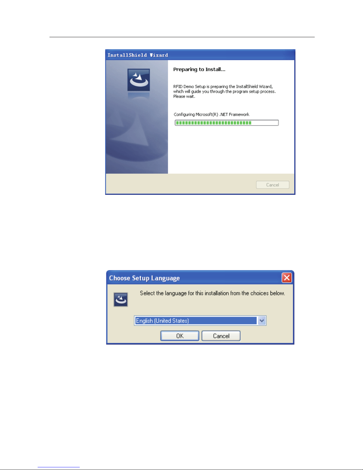
. If the system is not preinstalled with .NET
Framework 2.0, the system will automatically prompt the user to install .NET
Framework 2.0, as shown in the gure below:
Figure 3-1
Click on “Yes” to install .NET Framework 2.0:
3 DEMO user guide
User’s Manual
XC-RF850 Reader
27
Figure 3-2
STEP TWO:
Upon the completion of installation process, the screen will enter into Choose
Setup Language interface as shown in the gure below (if the system has been
pre-installed with .NET Framework 2.0, the screen will enter directly to the
Choose Setup Language interface), as shown below:
Figure 3-3
Select the setup language, Mandarin and English are both available.
Here, English is used as an example, click OK. The system starts to unzip folders
and this process requires several seconds. Upon completion, the screen will enter
into the following interface:
3 DEMO user guide

User’s Manual
XC-RF850 Reader
28
Figure 3-4
STEP THREE: Click on “Next”:
Figure 3-5
Enter user name and organization,
STEP FOUR: Click on “Next”:
3 DEMO user guide

User’s Manual
XC-RF850 Reader
29
Figure 3-6
Select the destination folder for the program. The default selection is: “E:
\Invengo\RFID Demo\”. If there is a need to change, please click on “Change…”
to customize and then click on “Next”:
Figure 3-7
STEP 5: Click on “Install”:
3 DEMO user guide

User’s Manual
XC-RF850 Reader
30
Figure 3-8
Installing…below shows the screen upon completion:
Figure 3-9
STEP 6: Click on “Finish” to complete the software installation. There will be a
“RFID Demo” shortcut appeared on the desktop.
3 DEMO user guide

User’s Manual
XC-RF850 Reader
31
3.3 Demo software operation
3.3.1 Demo initialization
During initial running Demo, the default mode is single reader mode. The
connected device operation is located on the central left of the main interface, as
shown in the gure below:
Figure 3-10
3.3.2 Connection
Click on “Conn” button as shown in the gure below:
Figure 3-11
3 DEMO user guide
User’s Manual
XC-RF850 Reader
32
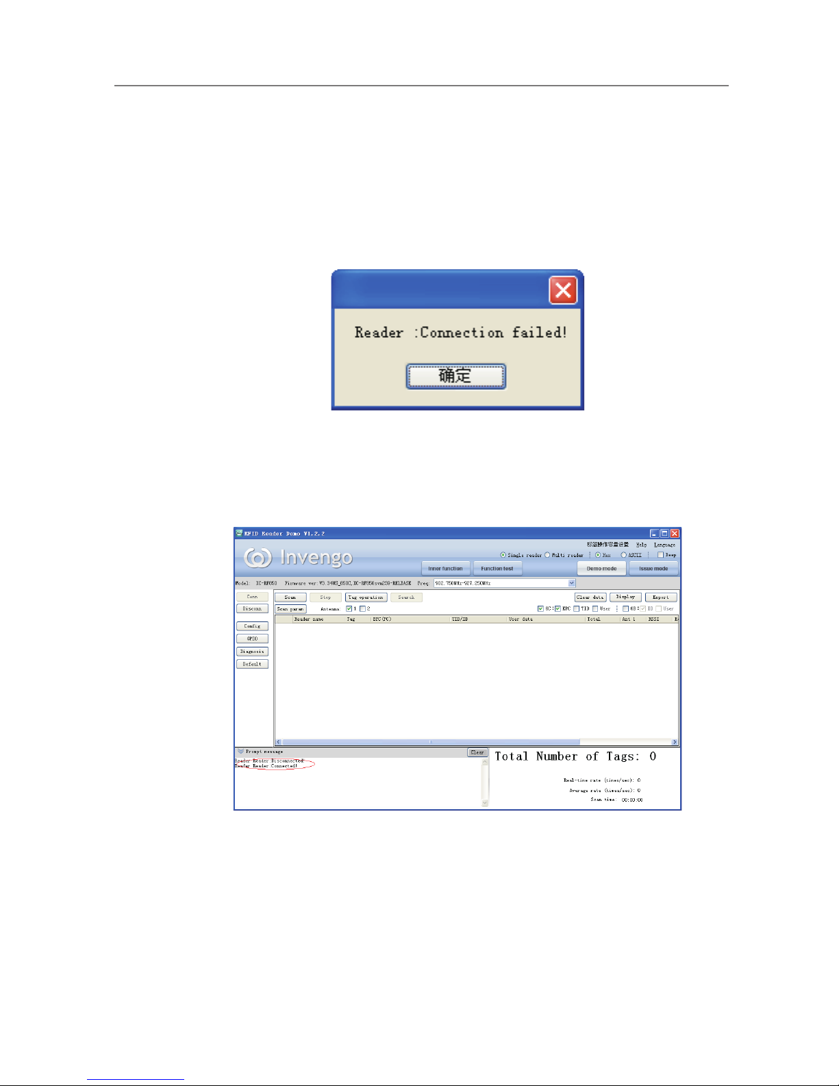
Please select connection method based on the actual scenario:
TCP/IP client (Network)
RS-232 (Serial)
Enter the control reader IP and port no. and click on “Conn.” Failure to connect
will be prompted.
Figure 3-12
If the connection is successful, the interface will disappear and the screen will
return to the single reader interface. Successful connection will be indicated on
the bottom left corner.
Figure 3-13
After successful connection, if there is a need to disconnect, click on
“Disconnect”.
3 DEMO user guide
User’s Manual
XC-RF850 Reader
33
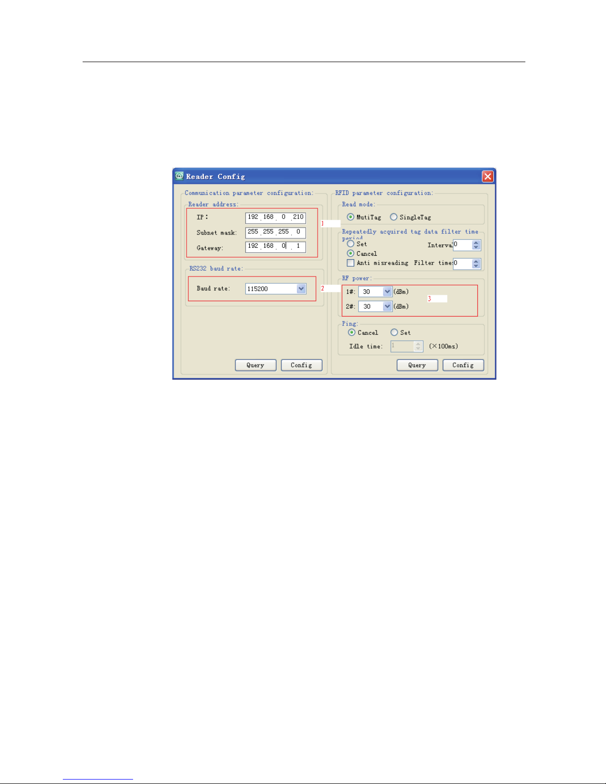
3.3.3 Reader conguration
To congure the reader, click on the reader conguration button, and a dialog
box will pop up. Set up the reader’s IP address, baud rate and related information
conguration of RFID, as shown in the gure below:
Figure 3-14
After completing conguration, click on “Cong” to save the conguration.
Click on “Query” to inquire about the current conguration of all connected
readers.
Reader address-1: Refers to the congured network parameters based on actual
needs (connecting reader in the same network segment)
Baud rate-2: Refers to the congured serial communication baud rate based on
actual needs.
RF port power-3: Refers to the congured RF port power based on actual needs.
Normally, the larger the power, the longer is the reading range.
Reading mode: SingleTag, suitable for the quick reading of single tag, in the case
of one tag within a RF antenna eld; MultiTag, suitable for the simultaneous
reading of multiple tags within a eld of RF antenna eld
Smart hibernation mode: The reader will enter into hibernation after being
idle for a period of time. The hibernation duration refers to the idle time in the
conguration. Otherwise, click on “Cancel” if no such conguration is needed.
3 DEMO user guide

User’s Manual
XC-RF850 Reader
34
3.3.4 Antenna choice
This reader has 2-channel antenna and these antenna can be formed random
combinations as shown in the gure below:
Figure 3-15
3.3.5 Scanning conguration
Scanning parameter setting as shown in the gure below:
Figure 3-16
6C tag reading conguration: Select the required 6C tag elds, including EPC,
TID, UserData
Tag reading parameter: Select reading method, available in loop reading and
single reading
Repeatedly acquired tag data lter time period: Similar tag upload time,
conguration and query
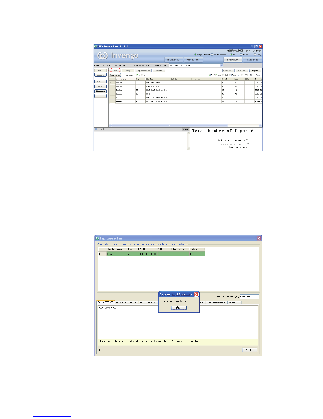
Tag operation
After conguring the reader as with 3.3.3 and 3.3.4 and 3.3.5, select the
corresponding tag type (6C tag), then click on “Scan” to scan the tag, as shown
in the gure below:
3 DEMO user guide
User’s Manual
XC-RF850 Reader
35
Figure 3-17
3.3.6 Tag operation
To perform EPC or user data area reading and writing operation on specic tag,
enter tag reading and writing interface (click on “Scan” → select scanned tag →
click on “Tag operation”). Main operations includes write EPC_6C, read user
data area_6C, write user data_6C, block operation_6C, as shown in the gure
below:
Figure 3-18
3 DEMO user guide

User’s Manual
XC-RF850 Reader
36
3.3.8 GPIO
Congure the reader I/O output port signal and the tag reading trigger condition
as well as the termination of tag reading trigger condition, as shown in the gure
below:
Figure 3-19
Query: Inquire on the status of all input ports.
Cong: Tick on the desired output ports to make modication before clicking on
“Cong” to save the conguration.
I/O trigger allows the reader to be trigger based on different status of I/O port, as
shown in the gure below:
Figure 3-20
Tag reading I/O trigger conguration:
Trigger port: Select the trigger port. There are two options available:
1#
2#
Query: Inquire on the conguration of selected input port.
Cong: Congure the trigger conguration of the selected input port.
3 DEMO user guide

User’s Manual
XC-RF850 Reader
37
Trigger condition: Available options shown below:
Close (turn off trigger condition)
Falling edge (level changes from high to low)
Rising edge trigger (level changes from low to high)
High level trigger (high steady state)
Low level trigger (low steady state)
Termination condition: Available in delay timing and port level.
Delay timing: Congure the continuous operating duration and cause the reader
to stop automatically once time runs up. Unit: 0.1 second.
Port level: Automatically select condition that contradicts the trigger condition.
Detailed explanation: I/O trigger is an automated tag reading function that is
based on I/O trigger condition and transfers the tag data to the host PC. There
are two trigger ports that can be congured independently. The tag reading
conguration is similar to the current reader scanning conguration.
Note: When conguring tag reading trigger, rst congure the scanning
conguration. Click on the scanning conguration, same as the setting in 3.4.5,
then congure the trigger port, trigger condition and termination condition.
3 DEMO user guide
User’s Manual
XC-RF850 Reader
38
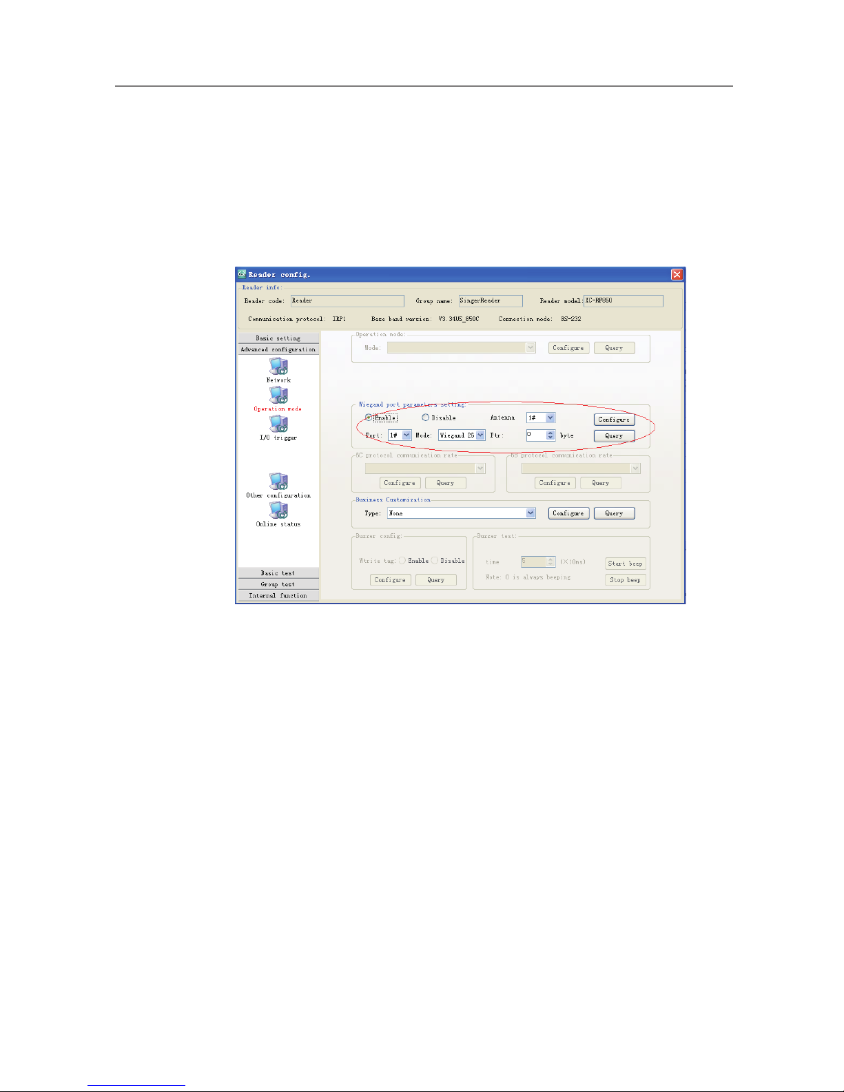
3.3.9 Operation mode
This section provides the option to modify the operatiiom mode. depending on
the work environment or operation requirements, select the desired mode.
Select the “Multiple readers -> Advanced conguration → Mode" (without this,
it says the reader does not support this feature ). It appears:
Figure 3-21
Screen appears. It automatically queries the current mode.
Wigan port parameter setting including: “Enable” and “Disable”, “Antenna”.
“Port”. “Type” and “Congure”
Antenna numbers include: 1# and 2#
Port numbers include: 1# and 2#
Type options include:
1. Wiegand 26: the rst 3 bytes of TID data reported from Wiegand port are
valid, and the last 5 bytes are zero.
2. Wigan 34: the rst 4 bytes of TID data reported from Wiegand port are valid,
and the last 4 bytes are zero.
3. Wigan 66: the rst 8 bytes of TID data reported from Wiegand port are valid.
Congure: acquire the start byte location of of data, 0 do not acquire.
3 DEMO user guide

User’s Manual
XC-RF850 Reader
39
3.3.10 Version Enquiry
Inquire the reader model and rmware version through RFID DEMO software,
as shown in the gure below:
Figure3-22
The denition of each information is as follows (this is just an example, subject
to changes with version upgrade):
Mode: XC-RF850 reader
Firmware version:
V3.34US_850C (RFID processor software version)
XC-RF850SVN239-RELEASE (Application processor software version)
Figure 3-23
V1.2.2 is the version of RFID DEMO software, as shown in gure 6-2
Explanation:
● For detailed introduction on the DEMO software operation, please refer to
“RFID Demo Software User Manual”.
3 DEMO user guide

User’s Manual
XC-RF850 Reader
40
4 Routine maintenance and service
4.1 Routine maintenance
● Check if the connection of the RF connector is good.
● Check if the connection of xed reader and antenna is good.
● Check if the external shield layer of RF cable joint is good.
● Check if the connection of reader power cord is good.
4.2 Troubleshooting and solution
During the application of XC-RF850 reader, users may encounter various
issues. This section consolidates all common issues during application and their
solutions.
1. ”Power” indicator does not light up after the power supply has
been switched on for 15 seconds
○ Check if the power supply from the power adapter is working normally.
Check also if the AC power voltage falls between 100V and 240V
○ Check if the power cord connection is poor or not properly connected
○ Check if the positive and negative terminal has been reversed
2. Unable to connect through Ethernet port
○ The default IP address of the reader under factory setting is: 192.168.0.210.
If the host PC’s IP address is belonged to the same network segment as the
reader, for example “192.168.0.XXX”, both devices will connect. If the
user forgot about the reader’s IP address, please look for a reader that is
connected to the host PC through RS-232 serial port (or USB serial port), and
recongure the IP address of the current reader.
3. Unable to connect through serial port
○ The baud rate of the reader is 115200bps. Once connected through serial port,
the baud rat should be 115200bps.
○ Check if the COM port selected in DEMO software DEMO is the COM port
of the host PC that is connected to the reader.
○ Check if the serial cable connection is proper. Any disconnection or insecure
4 Routine maintenance and service

User’s Manual
XC-RF850 Reader
41
connection will cause the command from the PC not being transferred to the
reader.
4. Unable to read tag
○ Check if the serial cable or the network cable is properly connected. Any
disconnection or insecure connection will cause the command from the PC
not being transferred to the reader.
○ Please check if both ends of the RF connector has been tightened. Check also
if the tag is damaged.
5. Tag reading and writing error
○ Check if the reader conguration in the application software is correct;
○ Check if the reader and the tag are compatible;
○ Check the tag position whether the tag is located within the effective reading
range of the reader;
○ Check if there is any electromagnetic interference between the readers and
other equipment;
○ Check if the tag is damaged.
6. Unsatisfactory reading/writing range
○ The positioning of antenna installation;
○ Interferences from the surrounding.
7. The reader fails to detect the tag
○ Check if the conguration of the antenna is correct. If the antenna is
connected to 1# RF port, 1# antenna must be chosen in the DEMO software.
○ Check if the tag is compatible with ISO18000-6C protocol. Any tag that is
not compatible with ISO18000-6C will not be detected.
○ Check if the tag is damaged. If the ID is undetected, please try with a different
reader and check if the tag has been damaged. If the data area remains
undetected, check if the tag data area has been locked. Locked tag needs to be
unlocked.
○ Check if the tag is located in the effective reading range of the reader.
○ Check if there is any electromagnetic interference between the readers or
other equipment.
8. Short tag reading distance
○ Check if the reader frequency setting is correct. If the antenna operating fre-
quency range is 902.75MHz - 927.25MHz, the hopping point selected for the
4 Routine maintenance and service

User’s Manual
XC-RF850 Reader
42
reader should not exceed the antenna’s operating frequency range (902.75MHz
- 927.25MHz). Otherwise it will affect the performance of the reader.
○ Check if the RF output power is low. The RF output power is adjustable.
○ Check if the polarization direction of the tag and the antenna is compatible. If
the antenna is vertically polarized, the tag must be placed vertically.
○ Check if the tag surface is covered with any other materials. If the tag surface
is covered with other material, the material may cause deviation in the
antenna’s frequency and affect the reading effect of the reader. If the material
is metallic, the reader will be unable to detect the tag, as RF signal is unable
to penetrate metal.
○ Check the RF cable connecting the reader and the antenna. If the connector of
the RF cable is loosened or broken, RF signal will become very weak and the
reading distance will be affected.
○ Check the properties of the tag. Metallic tag should be installed at metal
surface for the tag to function at full capacity. For other types of tag, please
avoid installation near metallic surface.
○ Normal aging of tag performance. Due to long term use, the tag performance
will decline and result in the shortening of the tag reading distance. However,
this will not affect normal usage. Only in the extreme case of aging where
the reading distance becomes extremely close and a replacement should be
considered.
4 Routine maintenance and service

User’s Manual
XC-RF850 Reader
43
5 Transportation and storage
5.1 Transport requirements
XC-RF850 meets all the standard requirements of road, rail, air, and water transportations.
5.2 Storage requirements
The long term storage of XC-RF850 must meet the following conditions:
● Ambient temperature: -30
o
C ~+75oC;
● Relative humidity: 5% ~90%RH;
● No abrupt temperature change, with the absence of acidic gas and other
harmful gases;
5 Transportation and storage
User’s Manual
XC-RF850 Reader
44
6 Packaging and Inspection
6 Packaging and Inspection
6.1 Packaging
XC-RF850 is packed in a box, and transported through large transport container.
Package size: 655mm×360mm×170mm
6.2 Inspection
In order to facilitate future storage and transport, keep the box and packaging
materials during inspection.
Apart from XC-RF861 reader, the package also contains the following accessories, as shown in the table below:
Table 6-1 Accessories List
No. Item Quantity Unit Order code Remark
1
Power supply and communication
cable _XC-RF850
1 Piece 2200700068 Standard
2 External IO cable _XC-RF850 1 Piece 2200700067 Standard
3 Output 24V/2.5A power adapter 1 Piece 1080200007 Standard
4 American Standard power line _1.8m 1 Piece 2200500027 Standard
5 RJ45 Network cable_1.5m 1 Piece 2200300003 Standard
6
Cross recessed countersunk head screw
Spring washer and at pad assembly
M5 * 10_ stainless steel _GB9074.4
4 Piece 1500100070 Standard
Holding rod mounting kit
7
L-shaped mounting bracket _XC-
RF850
1 Piece 2510900091
Standard8 U-shaped bolt M8x82_XC-RF850 2 Set 1500900028
9
Tooth shaped mounting bracket _XC-
RF850
2 Piece 2510900096
Wall mounting kit
10
Adjustable mounting bracket _XC-
RF850
1 Piece 2510900092
Optional
11 Flat washerΦ6_ stainless steel_GB97.1 4 Piece 1500500028

User’s Manual
XC-RF850 Reader
45
Shield plate mounting kit
12 Shield plate _XC-RF850 4 Piece 2510500079
Optional
13
type 1 Hexagon nut M4_ stainless
steel _GB6170
8 Piece 1500700015
14
Cross recessed countersunk head screw
Spring washer and at pad assembly
M4 * 10_ stainless steel _GB9074.4
8 Piece 1500100013
15 CD-ROM 1 Piece Standard
16 Product warranty card 1 Sheet Standard
17 Product certicate 1 Sheet Standard
Please check the product and its accessories according to the packing
list. Please contact your sales representative immediately if there is any
discrepancy or damage.
6 Packaging and Inspection

User’s Manual
XC-RF850 Reader
46
7 After-sales service
7 After-sales service
If you encounter any unsolvable problem when using our product, please contact
the customer service center.
Before a user engages our customer service center, please prepare the following
information at hand:
7.1 Other matters
If our customer service ofcer has conrmed with the user to return his/her
reader for maintenance, the user will receive a return merchandise authorization
(RMA) from our customer service ofcer. Please indicate the RMA no. on the
exterior of the return product packaging and, at the same time, provide the same
no. on a piece of paper and place it inside the packaging. This will ensure the
quick processing of the return product.
Please follow these steps when returning the handheld reader for maintenance:
● Carefully pack the reader and its accessories into the original antistatic foam
box. Please use a box with protective effect if the original box no longer
exists.
● Use ller to cover the products in the box.
● Place a note, written with RMA no., in the box.
● Indicate RMA no. and the word “fragile” on the exterior of the box.


Shenzhen HQ:
Corporate Headquarters
Invengo Information Technology Co., Ltd.
3/F, No.T2-B, High-tech Industrial Park South,
Shenzhen 518057, China
Tel: +86 800 830 7036
Fax: +86 755 2671 1693
Email: sales@invengo.cn
Website: www.invengo.cn
Singapore:
Invengo Technology Pte. Ltd.
10 Kallang Avenue, # 05-15 Aperia tower 2,
Singapore, 339510
Tel:+65 6702 3909
Email: invengo.sales@invengo.sg
Website: www.invengo.sg
US:
Invengo Technology Corp
2700-160 Sumner Blvd.
Raleigh, NC 27616, USA
Tel: +1 919 890 0202
Toll Free: +1 855 379 2725
Email: sales@invengo.com
Website: www.invengo.com
Europe:
Invengo Technology BV
Belder 30-A, 4704RK Roosendaal,
The Netherlands
Tel: +31 88 6363 793
Fax: +31 88 6363 794
Email: web@invengo.eu
Korea:
Invengo International Pte. Ltd (Korea)
30F ASEM Tower, 517 Yeongdong-daero,
Gangnam-gu, Seoul 135-798 Korea
Tel: +82 2 6001 3525
Fax: +82 2 6001 3003
Email: justin.kou@invengo.sg
 Loading...