

Page 1
Application Note 1507
Author: Marty Pandola
ZL6100EVAL2Z Dual Channel Evaluation Board
Description
The ZL6100 is an integrated mixed-signal power
conversion and management IC that combines an
efficient step-down DC/DC converter with key power and
thermal management functions in a single package. The
ZL6100 incorporates current sharing and adaptive
efficiency-optimization algorithms to provide a flexible,
efficient power IC building block.
The ZL6100EVAL2Z platform is a 6-layer board with two
power rails. One rail is a single phase, 30A power rail.
The other rail is a dual phase, 60A power rail
demonstrating the current sharing capability of the
ZL6100.
A USB to SMBus adapter board can be used to connect
the eval board to a PC. The PMBus command set is
accessed by using the Zilker Labs PowerNavigator™
evaluation software from a PC running Microsoft
Windows.
Features
• 30A Single-phase and 60A Dual-phase Rails
• Optimized for Efficiency
• Configurable Through SMBus
• Onboard Enable Switch
• Power Good Indicators
Target Specifications
•V
= 12V
IN
•V
•V
•f
• Efficiency: 90% at 50% load
• Output Ripple: ±1.5%
• Dynamic response: ±3%
(50%-70%-50% load step, di/dt = 2.5A/µs)
• Board Temperature: +25°C
= 1.8V/60A max
OUT1
= 1.5V/30A max
OUT2
= 300kHz
sw
SYNC
DDC
SMBus
TRACK
V
P3
IN
ENABLE
SW1
J10
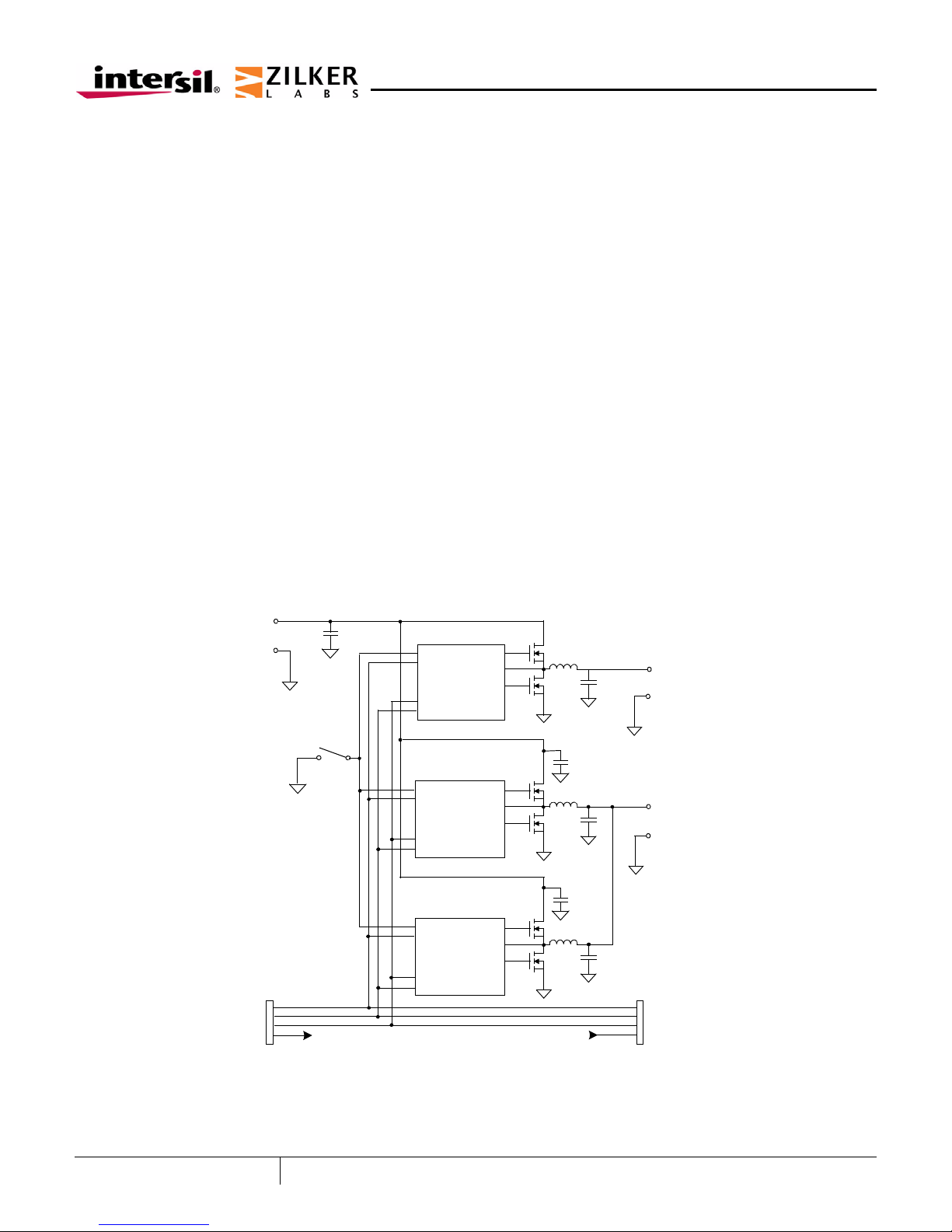
FIGURE 1. ZL6100EVAL2Z BLOCK DIAGRAM
EN
SYNC
ZL6100
SMBus
DDC
EN
SYNC
ZL6100
SMBus
DDC
EN
SYNC
ZL6100
SMBus
DDC
J11
P1
P2
SYNC
DDC
SMBus
PGVTRK PG
V
OUT2
V
OUT1
September 11, 2009
AN1507.0
1
CAUTION: These devices are sensitive to electrostatic discharge; follow proper IC Handling Procedures.
1-888-INTERSIL or 1-888-468-3774
| Intersil (and design) is a registered trademark of Intersil Americas Inc.
All other trademarks mentioned are the property of their respective owners.
Copyright Intersil Americas Inc. 2009. All Rights Reserved
Page 2

Application Note 1507
Functional Description
The ZL6100EVAL2Z provides all circuitry required to
demonstrate the features of the ZL6100. The
ZL6100EVAL2Z has a functionally-optimized ZL6100
circuit layout that allows efficient operation up to the
maximum output current. Power and load connections
are provided through plug-in sockets.
All features of the ZL6100 such as current sharing, softstart delay and ramp times, supply sequencing, voltage
tracking, and voltage margining are available on this
evaluation board. For voltage tr acking, the board is set
up for the single phase rail (V
phase rail (V
for configuring the board for other tracking combinations.
Figure 1 shows a functional block diagram of the
ZL6100EVAL2Z board. The SMBus address is selectable
through a jumper on the top side of the board. All power
to the board (VIN and I2C bus) must be removed before
changing the jumpers.
The hardware enable function is controlled by a toggle
switch on the ZL6100EVAL2Z board. The power good
(PG) LEDs indicate the correct state of PG when external
power is applied to the ZL6100EVAL2Z board. (Note: If a
USB board is connected to the ZL6100EVAL2Z and no
power is applied to the board, the PG LEDs will turn on
even though the power rails are not enabled.) The right
angle headers at opposite ends of the board are for
connecting a USB to SMBus adapter board or for daisy
chaining of multiple evaluation boards.
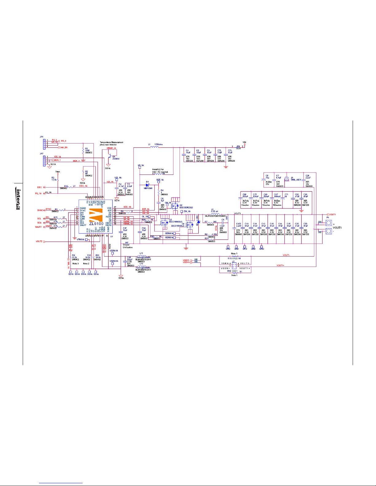
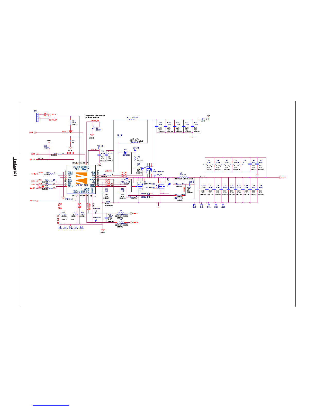
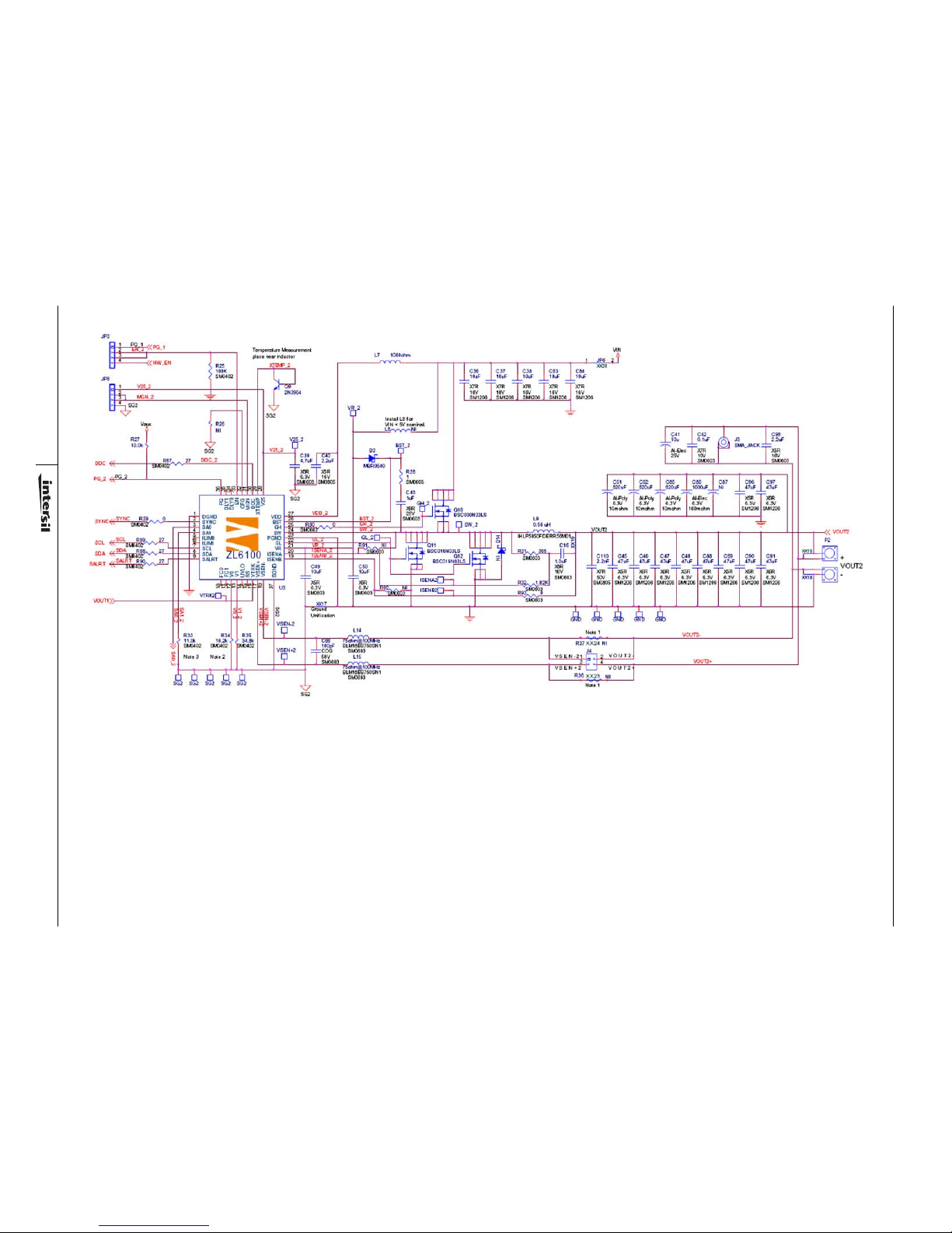
Figures 2 and 3 show the two phases of the 60A circuit.
Figure 4 shows the single phase operational circuit. The
circuit consists of the ZL6100 IC with its minimal
component count to realize a 30A buck converter. The
board layout has been optimized for thermal
performance.
Figure 5 is the Interface and Figure 9 SMBus address
selection circuitry .
). Contact the Zilker Labs sales office
OUT1
) to track the dual
OUT2
Operation
been pre-configured as described in this document, but
the user may modify the operating parameters through
the eval software or by loading a predefined scenario
from a configuration file.
Use the mouse-over pop-ups for PowerNavigator help.
™
Refer to Zilker Labs application note AN2033 “PMBus
Command Set DDC Products”, Intersil Corporation,
2009 for PMBus details.
The ENABLE switch can then be moved to “ENABLE” and
the ZL6100EVAL2Z board can be tested. Alternately , the
PMBus ON-OFF CONFIG and OPERATION commands may
be used.
Quick Start Guide
Stand Alone Operation
1. Set ENABLE switch to “DISABLE”
2. Apply load to VOUT+/VOUT- for each channel
3. Connect power supply to VIN+/VIN- (supply turned
off)
4. Turn power supply on
5. Set ENABLE switch to “ENABLE”
6. Monitor ZL6100EVAL2Z board operation using an
oscilloscope
USB (PMBus) Operation
1. Set ENABLE switch to “DISABLE”
2. Apply load to VOUT+/VOUT- for each channel
3. Connect power supply to VIN+/VIN- (supply turned
off)
4. Turn power supply on
5. Insert the Zilker Labs Eval Kit CD
6. Connect USB to SMBus adapter board to J10 of
ZL6100EVAL2Z
7. Connect supplied USB cable from computer to USB
to SMBus adapter board
a) Upon first-time connection, the Found New
Hardware Wizard will appear.
PMBus Operation
The ZL6100 utilizes the PMBus protocol. The PMBus
functionality can be controlled via USB from a PC running
the PowerNavigator evaluation software in a Windows XP
or Windows 2000/NT operating system.
Install the ZL6100EV AL2Z softw are u sing the CD
included in the ZL6100EVAL2Z kit.
For board operation, connect the included USB-to-SMBus
adapter board to J10 of the ZL6100EVAL2Z board.
Connect the desired load and an appropriate power
supply to the input and connect the included USB cable
to the PC running the PowerNavigator evaluation
software. Place the ENABLE switch in “DISABLE” and turn
on the power.
The evaluation software allows modification of all ZL6100
PMBus parameters. Each of the ZL6100 devices have
2
b) Windows XP users: Select ‘No’ at prompt to
search the Internet for drivers.
c) Follow the steps on the screen to install the
drivers from the CD.
8. Install the PowerNavigator evaluation software by
running setup.exe from the
PowerNavigator_installer folder on the CD.
9. Set ENABLE switch on EVB to “ENABLE”
10.Monitor and configure the ZL6100EVAL2Z board
using PMBus commands in the evaluation software
11.Test the ZL6100EVAL2Z operation using an
oscilloscope and the evaluation software.
September 11, 2009
AN1507.0
Page 3
3
AN1507.0
September 11, 2009
Board Schematics
FIGURE 2. ZL6100EVAL2Z 60A CURRENT SHARING RA IL (PHASE A) CIRCUIT
Application Note 1507
Page 4
4
AN1507.0
September 11, 2009
FIGURE 3. ZL6100EVAL2Z 60A CURRENT SHARING RAIL (PHASE B) CIRCUIT
Board Schematics (Continued)
Application Note 1507
Page 5
5
AN1507.0
September 11, 2009
FIGURE 4. ZL6100EVAL2Z 30A SINGLE PHASE RAIL CIRCUIT
Board Schematics (Continued)
Application Note 1507
Page 6
6
AN1507.0
September 11, 2009
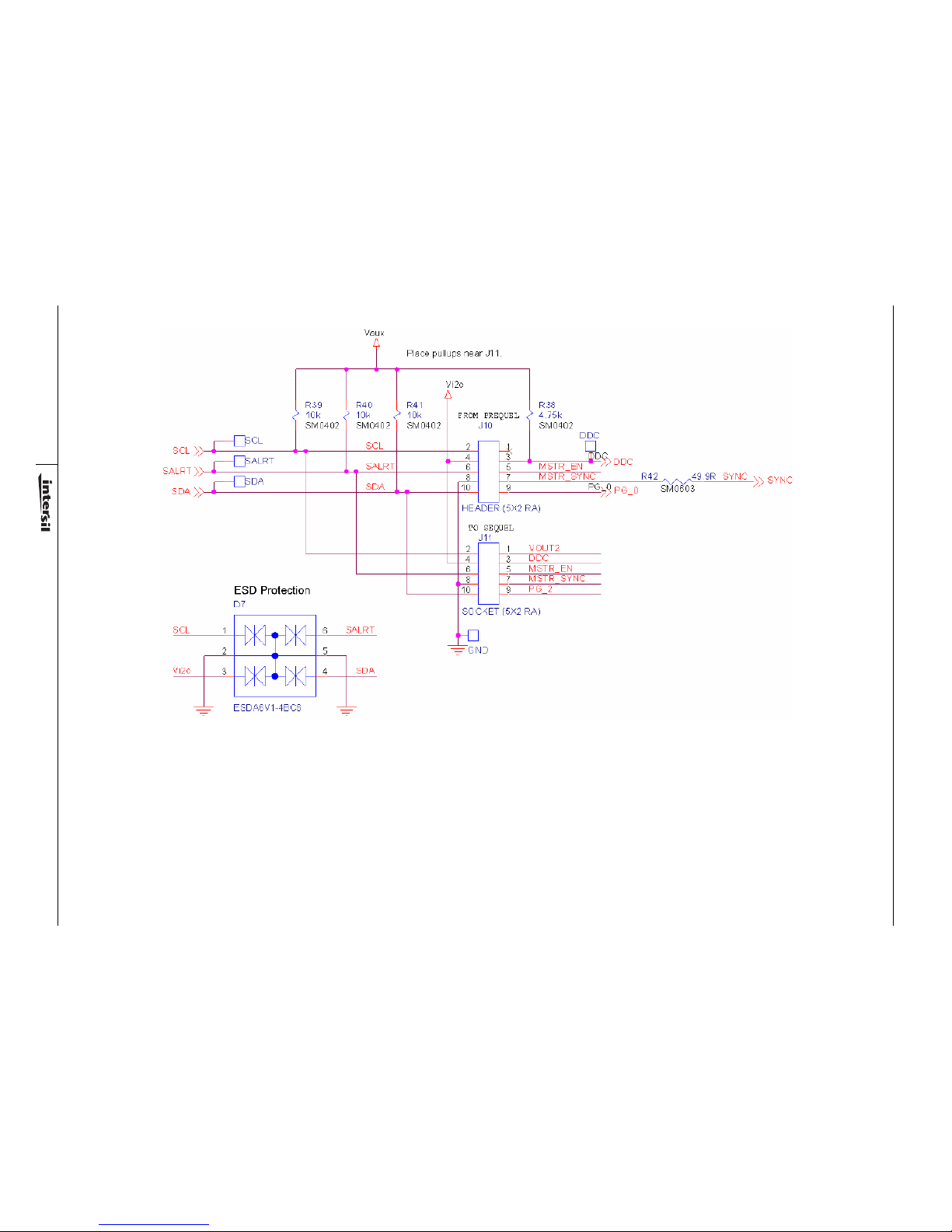
FIGURE 5. ZL6100EVAL2Z INTERFACE CIRCUITRY
Board Schematics (Continued)
Application Note 1507
Page 7
7
AN1507.0
September 11, 2009
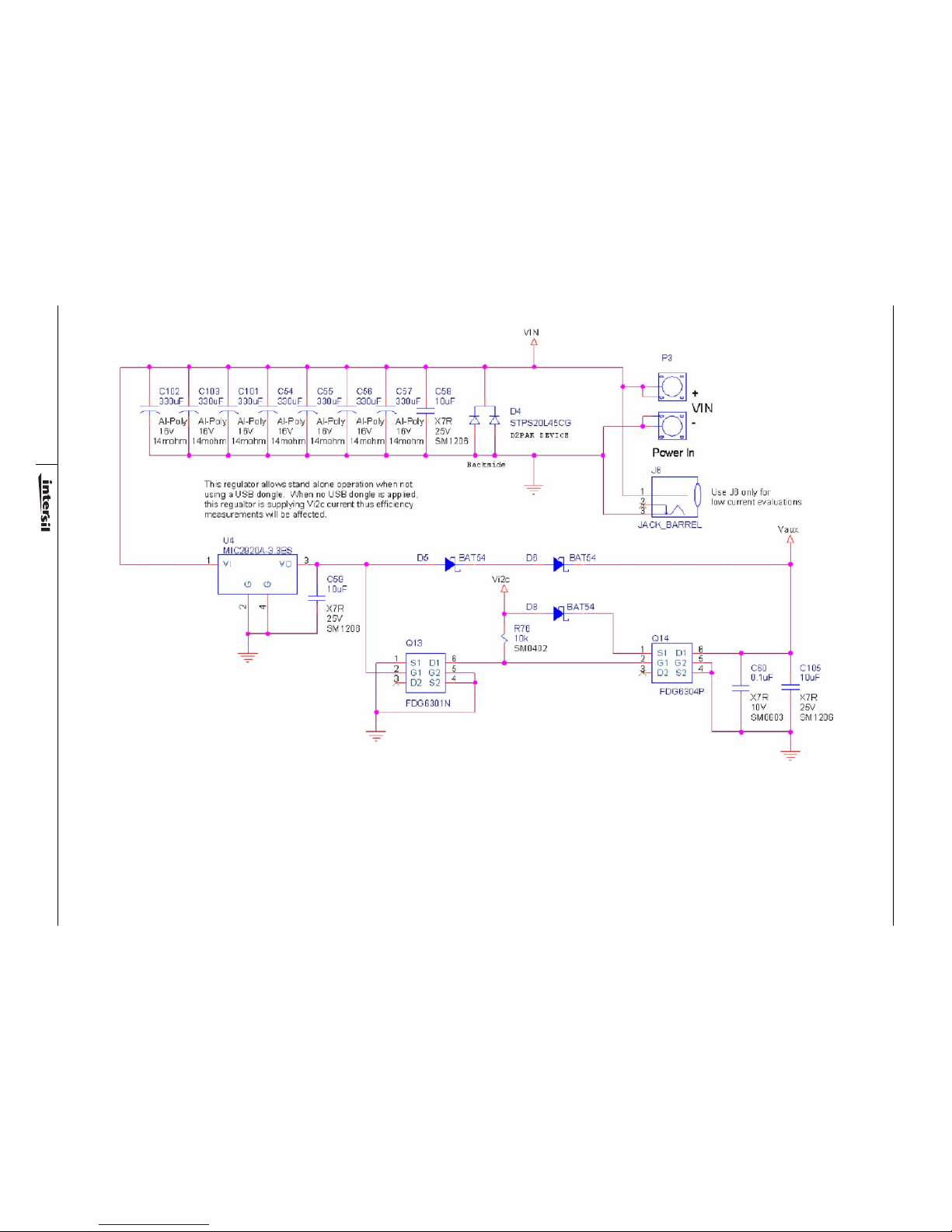
FIGURE 6. POWER-IN CIRCUIT
Board Schematics (Continued)
Application Note 1507
Page 8
8
AN1507.0
September 11, 2009
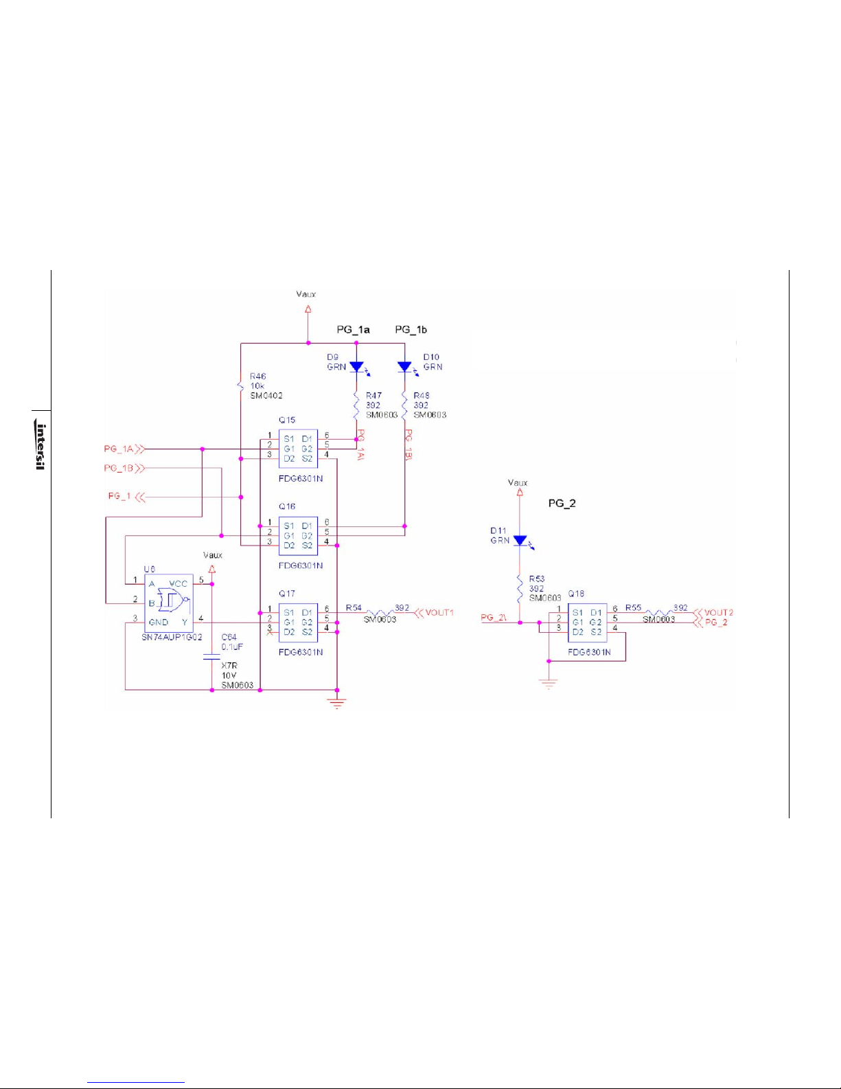
FIGURE 7. PG LED CIRCUITRY
Board Schematics (Continued)
Application Note 1507
Page 9
9
AN1507.0
September 11, 2009
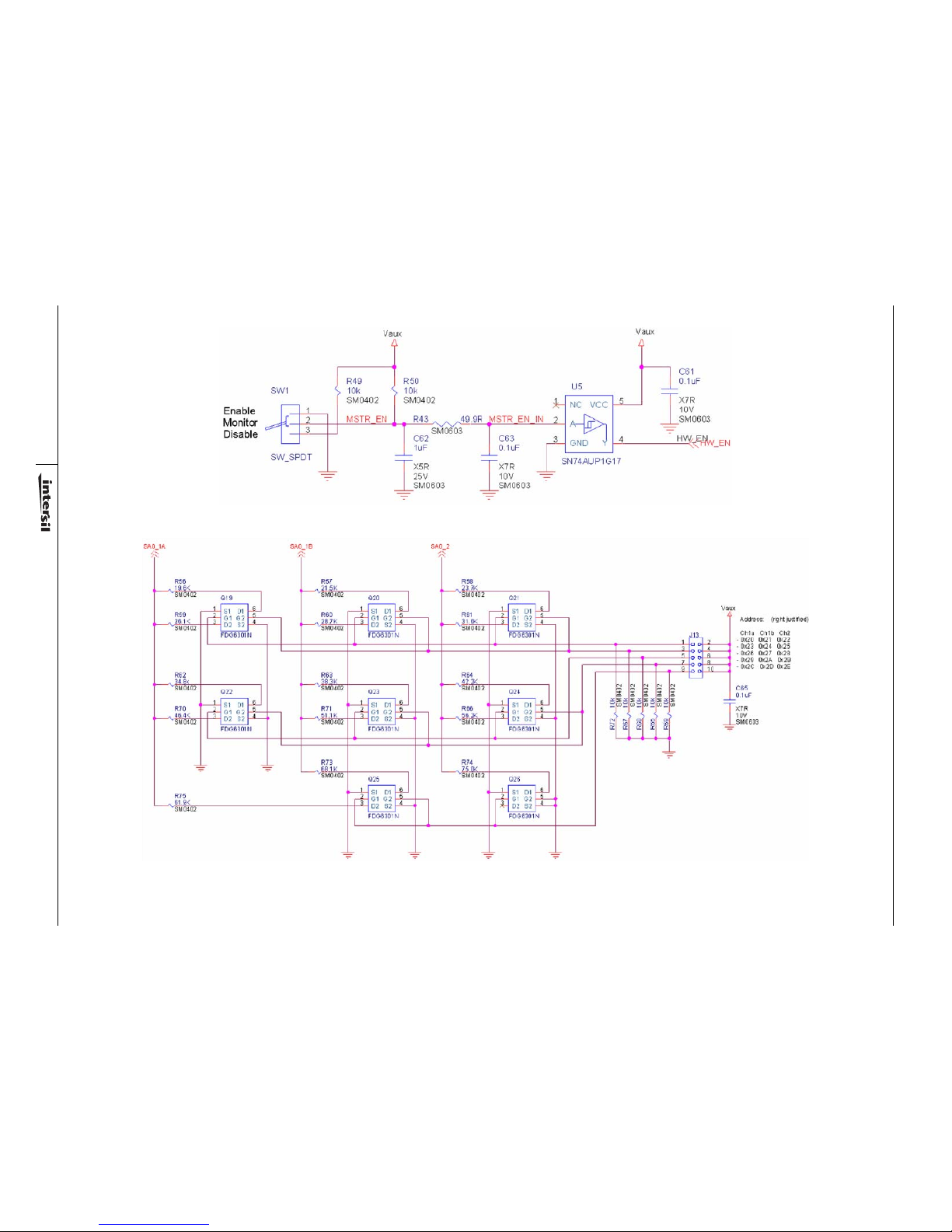
FIGURE 8. ENABLE SWITCH DEBOUNCE CIRCUIT
FIGURE 9. ADDRESS SELECTION CIRCUITRY
Board Schematics (Continued)
Application Note 1507
Page 10
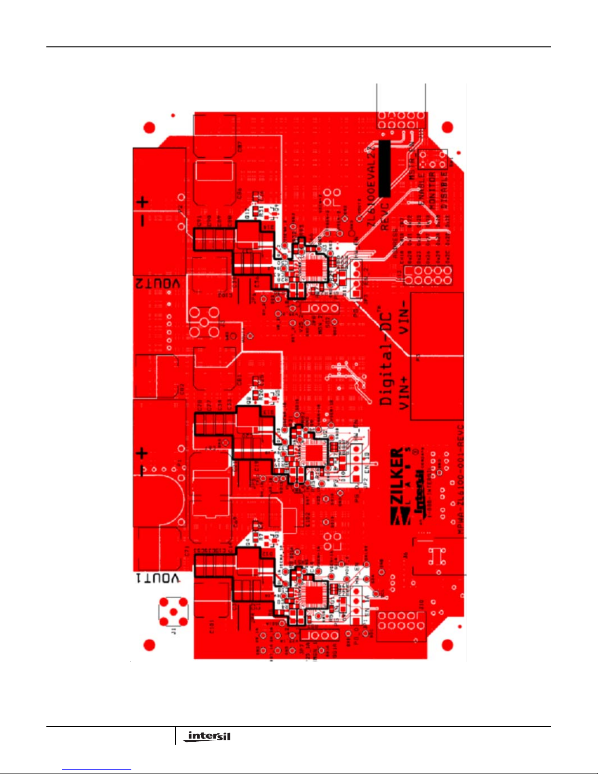
Board Layout – 6 Layers
Application Note 1507
10
FIGURE 10. PCB – TOP LAYER
September 11, 2009
AN1507.0
Page 11

Application Note 1507
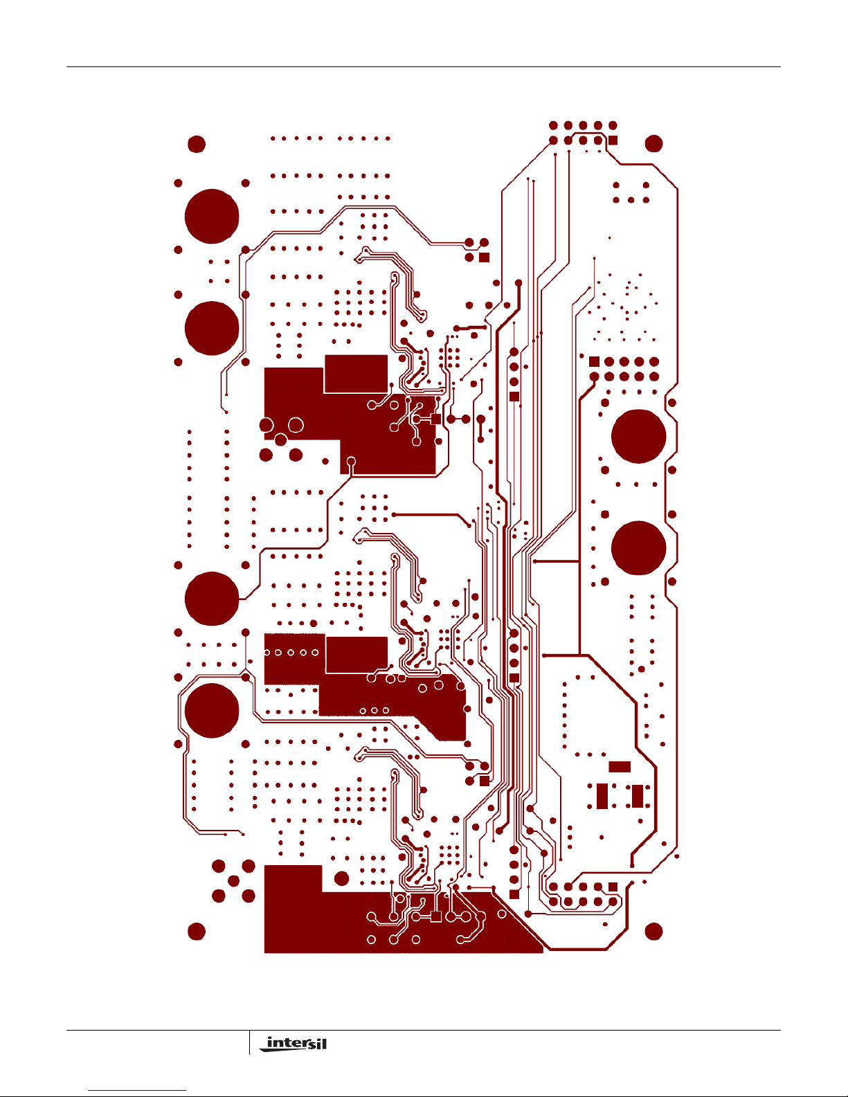
Board Layout – 6 Layers (Continued)
FIGURE 11. PCB – INNER LAYER 1 (VIEWED FROM TOP)
11
September 11, 2009
AN1507.0
Page 12
Application Note 1507
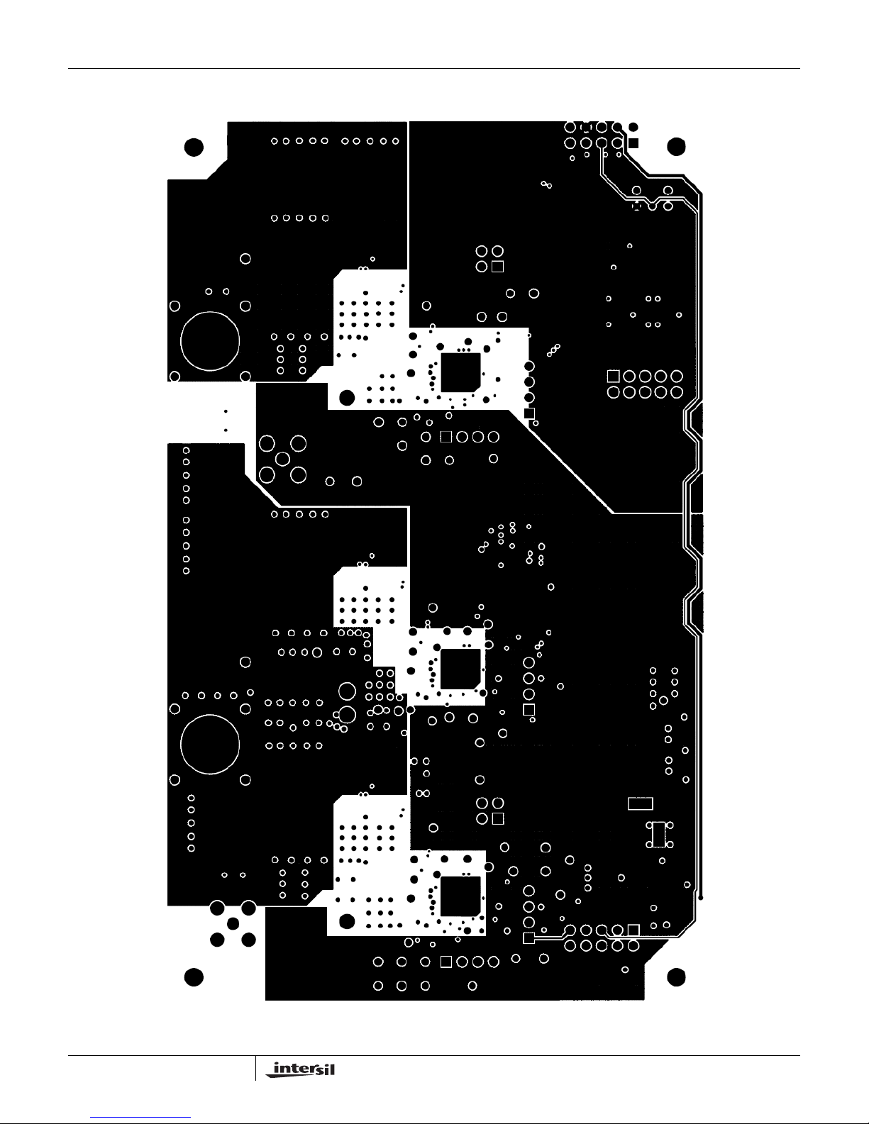
Board Layout – 6 Layers (Continued)
FIGURE 12. PCB – INNER LAYER 2 (VIEWED FROM TOP)
12
September 11, 2009
AN1507.0
Page 13
Application Note 1507
Board Layout – 6 Layers (Continued)
FIGURE 13. INNER LAYER 3 (VIEWED FROM TOP)
13
September 11, 2009
AN1507.0
Page 14

Application Note 1507
Board Layout – 6 Layers (Continued)
FIGURE 14. INNER LAYER 4 (VIEWED FROM TOP)
14
September 11, 2009
AN1507.0
Page 15

Application Note 1507
Board Layout – 6 Layers (Continued)
FIGURE 15. PCB – BOTTOM LAYER (VIEWED FROM TOP)
15
September 11, 2009
AN1507.0
Page 16

Application Note 1507
Board Layout – 6 Layers (Continued)
16
FIGURE 16. TOP ASSEMBLY DRAWING
September 11, 2009
AN1507.0
Page 17

Application Note 1507
Board Layout – 6 Layers (Continued)
17
FIGURE 17. BOTTOM ASSEMBLY DRAWING
September 11, 2009
AN1507.0
Page 18

Bill of Materials
Application Note 1507
PART NUMBER QTY UNIT
H1045-00104-16V10-T 7 ea C7, C42, C60, C61,
H1045-00105-25V10-T 7 ea C8, C9, C16, C24,
H1045-00106-6R3V20- T 6 ea C17, C18, C31, C32,
H1045-00225-16V10- T 2 ea C26, C98 CAP, SMD, 0603, 2.2µF ,
H1045-00475-6R3V10-T 3 ea C4, C22, C39 CAP, SMD, 0603, 4.7µF,
H1045-DNP 0 ea C44, C66, C99 CAP, SMD, 0603, DNPH
H1046-00225-25V10-T 3 ea C5, C23, C40 CAP, SMD, 0805, 2.2µF,
H1065-00106-25V10-T 18 ea a) C1, C2, C3, C19,
H1065-00106-25V10-T 0 ea b) C59, C72-C75,
H1065-00476-6R3V20-T 30 ea a) C10 to C15, C27
H1065-00476-6R3V20-T 0 ea b) C53, C77, C78,
APXA160ARA331MJC0G 7 ea C54, C55, C56, C57,
APXA6R3ARA821MJC0G 9 ea C51, C52, C68, C69,
EMVA250ADA100MD55G 2 ea C6, C41 CAP, SMD, 4x5.2, 10µF ,
EMZA6R3ADA102MHA0G 3 ea C67, C81, C86 CAP, SMD, 8x10,
EMZA6R3ADA102MHA0G 0 ea DNP (C71, C82,
IHLP5050FDERR56M01 3 ea L3, L6, L9 COIL-PWR INDUCTOR,
108-0740-001 6 ea P1, P2, P3 (2 EACH) CONN-JACK, BANANA-
142-0701-201 0 ea DNP (J1, J3) CONN-RF, SMA JACK,
REFERENCE
DESIGNATOR DESCRIPTION MFR NAME MFR PART
CAP , SMD, 0603, 0.1µF,
C63, C64, C65
C25, C43, C62
C49, C50
C20, C21, C36, C37,
C38, C58,
C83, C84, C105
to C30, C33 to C35,
C45 to C48,
C88 to C97
C101, C102, C103
C70, C76, C79, C80,
C85
C87)
16V, 10%, X7R, ROHS
CAP, SMD, 0603, 1µF,
25V, 10%, X5R, ROHS
CAP, SMD, 0603, 10µF,
6.3V, 20%, X5R, ROHS
16V, 10%, X5R, ROHS
6.3V, 10%, X5R, ROHS
PLACE HOLDER, ROHS
25V, 10%, X5R, ROHS
CAP, SMD, 1206, 10µF,
25V, 10%, X5R, ROHS
CAP, SMD, 1206,
10µF,25V, 10%, X5R,
ROHS
CAP, SMD, 1206, 47µF,
6.3V, 20%, X5R, ROHS
CAP, SMD, 1206, 47µF,
6.3V, 20%, X5R, ROHS
CAP, SMD, 10x12,
330µF, 16V, 20%,
14mΩ, ALUM. ELEC .,
ROHS
CAP, SMD, 10x12,
820µF, 6.3V, 20%,
10mΩ, ALUM. ELEC .,
ROHS
25V, 20%, ALUM.
ELEC., ROHS
1000µF, 6.3V, 20%,
ALUM. ELEC., ROHS
CAP, SMD, 8x10,
1000µF, 6.3V, 20%,
ALUM. ELEC., ROHS
SMD, 13mm, 0.56µH,
20%, 37A, ROHS
SS-SDRLESS,
VERTICAL, ROHS
50Ω, BMT, ST
MURATA GRM39X7R104K016AD
MURATA GRM188R61E105KA12D
TDK C1608X5R0J106M
MURATA GRM188R61C225KE15D
VENKEL C0603X5R6R3-475KNE
PANASONIC ECJ-2FB1E225K
VENKEL C1206X5R250-106KNE
VENKEL C1206X5R250-106KNE
MURATA GRM31CR60J476ME19L
MURATA GRM31CR60J476ME19L
NIPPON
CHEMI-CON
NIPPON
CHEMI-CON
NIPPON
CHEMI-CON
NIPPON
CHEMI-CON
NIPPON
CHEMI-CON
VISHAY IHLP5050FDERR56M01
JOHNSON COMPONENTS 108-0740-001
JOHNSON COMPONENTS 142-0701-201
APXA160ARA331MJC0G
APXA6R3ARA821MJC0G
EMVA250ADA100MD55G
EMZA6R3ADA102MHA0G
EMZA6R3ADA102MHA0G
18
September 11, 2009
AN1507.0
Page 19

Application Note 1507
Bill of Materials (Continued)
REFERENCE
PART NUMBER QTY UNIT
3-644456-4 3 ea JP1, JP2, JP3 CONN-HEADER, 1x4,
881545-2 4 ea a) JP1-Pins 3 and 4,
881545-2 0 ea b) JP3-Pins 3 and 4,
PJ-002A 1 ea J6 CONN-POWER JACK,
SSQ-105-02-T-D-RA 1 e a J11 CONN-SOCKET STRIP,
TSW-105-07-T-D 1 ea J13 CONN-HEADER, 2x5,
TSW-105-08-T-D-RA 1 ea J10 CONN-HEADER, 2X5,
BAT54XV2T1G-T 3 ea D5, D6, D8 DIODE-SCHOTTKY,
MBR0540T1G-T 3 ea D1, D2, D3 DIODE-RECTIFIER,
STPS20L45CG 1 ea D4 DIODE-RECTIFIER,
CMD17-21VGC/TR8-T 3 ea D9, D10, D11 LED, SMD, 0805,
BLM18BB750SN1-T 6 ea L10, L11, L12, L13,
BLM21AG102SN1D-T 0 ea DNP (L2, L5, L8) FERRITE CHIP, SMD,
BLM21AG102SN1D-T 3 ea L1, L4, L7 FERRITE CHIP, SMD,
ESDA6V1-4BC6 1 ea D7 DIODE- TV S, ESD , QU AD
MIC2920A-3.3WS 1 ea U4 IC-LDO REGULATOR,
SN74AUP1G02DCKR 1 ea U6 IC-SINGLE 2-INPUT
DESIGNATOR DESCRIPTION MFR NAME MFR PART
VERTICAL, TIN, WHT
NYLON, ROHS
JP2-Pins 3 and 4,
J13-Pins 1 and 2
L14, L15
CONN-JUMPER, SHUNT
LP W/HANDLE, 2P,
2.54mm, BLK, ROHS
CONN-JUMPER, SHUNT
LP W/HANDLE, 2P,
2.54mm, BLK, ROHS
TH, 2.1mm, 16V@2.5A,
BLK, R/A, ROHS
TH, 2x5, 2.54mm, TIN,
R/A, ROHS
BRKAWY , 2.54mm, TIN ,
ROHS
BRKAWY, 2.54mm, TIN,
R/A, ROHS
SMD, 2P, SOD523, 30V ,
200mA, ROHS
SMD, SOD-123, 2P,
40V, 0.5A, ROHS
SCHOTTKY, SMD,
D2PAK, 45V, 10A, ROHS
GREEN, CLEAR, 10mcd,
2.1V, 20mA, 570nm,
ROHS
FERRITE CHIP, SMD,
0603,75Ω, 25%,
300mA, 0.7Ω, ROHS
0805, 1000Ω, 200mA,
100MHz, ROHS
0805, 1000Ω, 200mA,
100MHz, ROHS
BI-DIRECTIONAL, 6P,
SOT23-6L, 80W, ROHS
4P, SOT-223, 3.3V,
400mA, ROHS
POSITIVE-NOR GATE,
SMD, 5P, SC70-5, ROHS
AMP/TYCO 3-644456-4
TYCO
ELECTRONICS
TYCO
ELECTRONICS
CUI, INC PJ-002A
SAMTEC SSQ-105-02-T-D-RA
SAMTEC TSW-105-07-T-D
SAMTEC TSW-105-08-T-D-RA
ON
SEMICONDUCTOR
ON
SEMICONDUCTOR
STMICRO
ELECTRONICS
CHICAGO
MINIATURE
MURATA BLM18BB750SN1
MURATA BLM21AG102SN1D
MURATA BLM21AG102SN1D
STMICRO
ELECTRONICS
MICREL MIC2920A-3.3WS
TEXAS
INSTRUMENTS
881545-2
881545-2
BAT54XV2T1G
MBR0540T1G
STPS20L45CG
CMD17-21VGC/TR8
ESDA6V1-4BC6
SN74AUP1G02DCKR
19
September 11, 2009
AN1507.0
Page 20

Application Note 1507
Bill of Materials (Continued)
REFERENCE
PART NUMBER QTY UNIT
SN74AUP1G17DCKR 1 ea U5 IC-BUFFER, SCHMITT
ZL6100ALNFT 3 ea U1, U2, U3 IC-DIGITAL DC-DC
BSC016N03LSG 6 ea Q3, Q4, Q7, Q8,
BSC030N03LS G 3 ea Q2, Q6, Q10 TRANSISTOR-MOS,
FDG6301N-T 13 ea Q13, Q15 to Q26 TRANSIST-MOS, DUAL
FDG6304P 1 ea Q14 TRANSIST-MOS , DUAL
MMBT3904LT1G-T 3 ea Q1, Q5, Q9 TRANSISTOR, NPN,
H2510-00R00-1/16W-T 15 ea R5, R17, R29, R52,
H2510-01002-1/16W1-T 15 ea a) R3, R16, R27,
H2510-01002-1/16W1-T 0 ea b) R65, R67, R68,
H2510-01003-1/16W1- T 3 ea R1, R14, R25 RES, SMD, 0402, 100k,
H2510-01102-1/16W1-T 3 ea R9, R22, R33 RES, SMD, 0402, 11k,
H2510-01622-1/16W1- T 3 ea R10, R23, R34 RES, SMD, 0402, 16.2k,
H2510-01962-1/16W1- T 1 ea R56 RES, SMD, 0402, 19.6k,
H2510-02152-1/16W1- T 1 ea R57 RES, SMD, 0402, 21.5k,
H2510-02372-1/16W1- T 1 ea R58 RES, SMD, 0402, 23.7k,
H2510-02612-1/16W1- T 1 ea R59 RES, SMD, 0402, 26.1k,
H2510-02701-1/16W1-T 1 ea R38 RES, SMD, 0402, 2.7k,
H2510-02872-1/16W1- T 1 ea R60 RES, SMD, 0402, 28.7k,
DESIGNATOR DESCRIPTION MFR NAME MFR PART
TRIGGER, 5P, SC-70-5,
3.6V, 4mA, ROHS
CONTROLLER, 36P,
QFN, 6x6, ROHS
Q11, Q12
R77, R78, R79, R83
to R90
R39, R40, R41, R46,
R49, R50,
R69, R72, R76
TRANSIST-MOS,
N-CHANNEL, 8P,
PG-TDSON-8, 30V,
100A, ROHS
N-CHANNEL, 8P,
PG-TDSON-8, 30V,
100A, ROHS
N-CHANNEL, SMD,
SC70-6, 25V, 220mA,
ROHS
P-CHANNEL, 6P,
SC70-6, -25V, -0.41A,
ROHS
SOT-23, 3P, 40V,
0.2A.0.35W, ROHS
RES, SMD, 0402, 0Ω,
1/16W, 5%, TF, ROHS
RES, SMD, 0402, 10k,
1/16W, 1%, TF, ROHS
RES, SMD, 0402, 10k,
1/16W, 1%, TF, ROHS
1/16W, 1%, TF, ROHS
1/16W, 1%,TF, ROHS
1/16W, 1%, TF, ROHS
1/16W, 1%, TF, ROHS
1/16W, 1%, TF, ROHS
1/16W, 1%, TF, ROHS
1/16W, 1%, TF, ROHS
1/16W, 1%, TF, ROHS
1/16W, 1%, TF, ROHS
TEXAS
INSTRUMENTS
INTERSIL ZL6100ALNFT
INFINEON
TECHNOLOGY
INFINEON
TECHNOLOGY
FAIRCHILD FDG6301N
FAIRCHILD FDG6304P
ON
SEMICONDUCTOR
VENKEL CR0402-16W-00T
PANASONIC ERJ-2RKF1002X
PANASONIC ERJ-2RKF1002X
PANASONIC ERJ2RKF1003
PANASONIC ERJ-2RKF1102V
PANASONIC ERJ-2RKF1622
PANASONIC ERJ-2RKF1962
PANASONIC ERJ-2RKF2152X
PANASONIC ERJ-2RKF2372V
VENKEL CR0402-16W-2612FT
VENKEL CR0402-16W-2701FT
PANASONIC ERJ-2RKF2872X
SN74AUP1G17DCKR
BSC016N03LSG
BSC030N03LS G
MMBT3904LT1G-T
20
September 11, 2009
AN1507.0
Page 21

Application Note 1507
Bill of Materials (Continued)
REFERENCE
PART NUMBER QTY UNIT
H2510-03162-1/16W1- T 1 ea R61 RES, SMD, 0402, 31.6k,
H2510-03482-1/16W1-T 4 ea R11, R24, R35, R62 RES, SMD, 0402, 34.8k,
H2510-03832-1/16W1- T 1 ea R63 RES, SMD, 0402, 38.3k,
H2510-04222-1/16W1- T 1 ea R64 RES, SMD, 0402, 42.2k,
H2510-04642-1/16W1- T 1 ea R70 RES, SMD, 0402, 46.4k,
H2510-05112-1/16W1- T 1 ea R71 RES, SMD, 0402, 51.1k,
H2510-05622-1/16W1- T 1 ea R66 RES, SMD, 0402, 56.2k,
H2510-06192-1/16W1- T 1 ea R75 RES, SMD, 0402, 61.9k,
H2510-06812-1/16W1- T 1 ea R73 RES, SMD, 0402, 68.1k,
H2510-07502-1/16W1-T 1 ea R74 RES, SMD, 0402, 75k,
H2510-DNP 0 ea R2, R15, R26 RES, SMD, 0402, DNP,
H2511-00010-1/10W1-T 2 ea R4, R18 RES, SMD, 0603, 1Ω,
H2511-00R00-1/10W-T 7 ea R6, R19, R28, R30,
H2511-01871-1/10W1- T 3 ea R8, R21, R32 RES, SMD, 0603, 1.87k,
H2511-03650-1/10W1- T 3 ea R7,R20,R31 RES, SMD, 0603, 365Ω,
H2511-03920-1/10W1- T 5 ea R47, R48, R53, R54, RES, SMD, 0603, 392Ω,
H2511-049R9-1/10W1- T 2 ea R42, R43 RES, SMD, 0603, 49.9 Ω,
H2511-DNP 0 ea R12, R13, R36, R37,
G13AP-RO 1 ea SW1 SWITCH-TOGGLE,
4-40X1/4-SCREW-SS 4 ea Four corners SCREW, 4-40x1/4in,
DNP 0 ea C100, C104, C110 DO NOT POPULATE OR
DNP 0 ea D12, D13, D14 DO NOT POPULATE OR
DESIGNATOR DESCRIPTION MFR NAME MFR PART
1/16W, 1%, TF, ROHS
1/16W, 1%, TF, ROHS
1/16W, 1%, TF, ROHS
1/16W, 1%, TF, ROHS
1/16W, 1%, TF, ROHS
1/16W, 1%, TF, ROHS
1/16W, 1%, TF, ROHS
1/16W, 1%, TF, ROHS
1/16W, 1%, TF, ROHS
1/16W, 1%, TF, ROHS
DNP, DNP, TF, ROHS
1/10W, 1%,TF, ROHS
RES, SMD, 0603, 0Ω,
R51, R82, R93
R44, R45, R80, R81,
R91, R92
1/10W, TF, ROHS
1/10W, 1%, TF, ROHS
1/10W, 1%, TF, ROHS
1/10W, 1%, TF, ROHS
1/10W, 1%, TF, ROHS
RES, SMD, 0603,
DNP-PLACE HOLDER,
ROHS
THRU-HOLE, 5P, SPDT,
3POS, ON-OFF-ON,
ROHS
PHILLIPS, PAN,
STAINLESS STEEL,
ROHS
PURCHASE
PURCHASE
VENKEL CR0402-16W-3162FT
PANASONIC ERJ-2RKF3482
PANASONIC ERJ-2RKF3832
PANASONIC ERJ-2RKF4222X
PANASONIC ERJ2RKF4642
PANASONIC ERJ-2RKF5112X
PANASONIC ERJ-2RKF5622
VENKEL CR0402-16W-6192FT
VENKEL CR0402-16W-6812FT
VENKEL CR0402-16W-7502FT
PANASONIC ERJ-3RQF1R0V
VENKEL CR0603-10W-000T
VENKEL CR0603-10W-1871FT
VENKEL CR0603-10W-3650FT
PANASONIC ERJ-3EKF3920V
VENKEL CR0603-10W-49R9FT
NKK G13AP-RO
KEYSTONE 9900
21
September 11, 2009
AN1507.0
Page 22

Application Note 1507
Bill of Materials (Continued)
REFERENCE
PART NUMBER QTY UNIT
DNP 0 ea J2, J4 DO NOT POPULATE OR
DNP 0 ea JP4, JP5, JP6, JP7,
DNP 0 ea a) TP1-TP10 ,TP12-
DNP 0 ea b) TP48 to TP56,
DNP 0 ea c) TP70 to TP75 DO NOT POPULATE OR
VC-234-8 6 ea P1, P2, P3 (COVER
H1045-00104-16V10-T 7 ea C7, C42, C60, C61,
DESIGNATOR DESCRIPTION MFR NAME MFR PART
PURCHASE
DO NOT POPULATE OR
JP8
TP40, TP42, TP43,
TP46,
TP58 to TP65, TP67,
TP68,
BOTTOMS OF
POSTS)
C63, C64, C65
PURCHASE
DO NOT POPULATE OR
PURCHASE
DO NOT POPULATE OR
PURCHASE
PURCHASE
CAPLUG-ROUND VINYL
CLOSURE, FLEXIBLE,
0.5x0.234, ROHS
CAP , SMD , 0603, 0.1µF,
16V, 10%, X7R, ROHS
CAPLUGS VC-234-8
MURATA GRM39X7R104K016AD
22
September 11, 2009
AN1507.0
Page 23

Application Note 1507
Default Configuration Text
The following text is loaded into the ZL6100 devices on the EV2 as default settings. Each PMBus command is loaded
via the PowerNavigator software. The # sy mbol is used for a comment line.
# Configuration file for ZL6100EVAL2Z-Ch1A
#Erase default and user stores
RESTORE_FACTORY
STORE_USER_ALL
STORE_DEFAULT_ALL
RESTORE_DEFAULT_ALL
MFR_ID Zilker_Labs
MFR_MODEL ZL6100EVAL2ZR2
MFR_REVISION Cfg Rev 1.1
MFR_LOCATION Austin_TX
MFR_DATE 08_27_09
MFR_SERIAL ch1A
VOUT_COMMAND 1.80
VOUT_DROOP 0.5
VOUT_UV_FauLT_LIMIT 1.53
VOUT_UV_FAULT_RESPONSE 0x80
VOUT_OV_FauLT_LIMIT 2.07
VOUT_OV_FAULT_RESPONSE 0x80
OVUV_CONFIG 0x80
IOUT_SCALE 1.13
IOUT_CAL_OFFSET 1.00
IOUT_OC_FAULT_LIMIT 45.0
IOUT_AVG_OC_FAULT_LIMIT 40.0
IOUT_UC_FAULT_LIMIT -40.0
IOUT_AVG_UC_FAULT_LIMIT -40.0
MFR_IOUT_OC_FAULT_RESPONSE 0xBF
MFR_IOUT_UC_FAULT_RESPONSE 0xBF
VIN_OV_FAULT_LIMIT 14.0
VIN_OV_WARN_LIMIT 13.5
VIN_OV_FAULT_RESPONSE 0x80
VIN_UV_WARN_LIMIT 4.641
VIN_UV_FAULT_LIMIT 4.50
VIN_UV_FAULT_RESPONSE 0x80
OT_FAULT_RESPONSE 0xBF
UT_FAULT_RESPONSE 0xBF
POWER_GOOD_ON 1.35
POWER_GOOD_DELAY 10.0
TON_DELAY 15
TON_RISE 5
TOFF_DELAY 15
TOFF_FALL 5
23
September 11, 2009
AN1507.0
Page 24

Application Note 1507
DEADTIME 0x3838
DEADTIME_CONFIG 0x0606
MAX_DUTY 96
INDUCTOR 0.56
FREQUENCY_SWITCH 300 # kHz
#CompZL Taps for G=36, Q=0.25, f=3.5kHz, fsw=300kHz, Vi=12, Vo=1.8
PID_TAPS A=13553.75, B=-23599.50, C=10109.25 # dIo=30-45A @ 2.5A/us, dVo=+/-3%
# Advanced
USER_CONFIG 0x6050 # SYNC Input
MFR_CONFIG 0x82D4
INTERLEAVE 0x0000
TEMPCO_CONFIG 0xA4
TRACK_CONFIG 0x00
# Advanced 2
MISC_CONFIG 0x4080
ISHARE_CONFIG 0x0121 # Ishare Group 1, members 2, position 1, CS En
DDC_CONFIG 0x0101 # DDC Rail ID 1, Broadcast Group 1
DDC_GROUP 0x00000000
STORE_DEFAULT_ALL
RESTORE_DEFAULT_ALL
-------------------------------------------------------------------------------------# Configuration file for ZL6100EVAL2Z-Ch1B
#Erase default and user stores
RESTORE_FACTORY
STORE_DEFAULT_ALL
STORE_USER_ALL
RESTORE_DEFAULT_ALL
MFR_ID Zilker_Labs
MFR_MODEL ZL6100EVAL2ZR2
MFR_REVISION Cfg Rev 1.1
MFR_LOCATION Austin_TX
MFR_DATE 08_27_09
MFR_SERIAL ch1B
VOUT_COMMAND 1.80
VOUT_DROOP 0.5
VOUT_UV_FauLT_LIMIT 1.53
VOUT_UV_FAULT_RESPONSE 0x80
VOUT_OV_FauLT_LIMIT 2.07
VOUT_OV_FAULT_RESPONSE 0x80
OVUV_CONFIG 0x80
IOUT_SCALE 1.13
IOUT_CAL_OFFSET 1.00
IOUT_OC_FAULT_LIMIT 45.0
IOUT_AVG_OC_FAULT_LIMIT 40.0
IOUT_UC_FAULT_LIMIT -40.0
24
September 11, 2009
AN1507.0
Page 25

Application Note 1507
IOUT_AVG_UC_FAULT_LIMIT -40.0
MFR_IOUT_OC_FAULT_RESPONSE 0xBF
MFR_IOUT_UC_FAULT_RESPONSE 0xBF
VIN_OV_FAULT_LIMIT 14.0
VIN_OV_WARN_LIMIT 13.5
VIN_OV_FAULT_RESPONSE 0x80
VIN_UV_WARN_LIMIT 4.641
VIN_UV_FAULT_LIMIT 4.50
VIN_UV_FAULT_RESPONSE 0x80
OT_FAULT_RESPONSE 0xBF
UT_FAULT_RESPONSE 0xBF
POWER_GOOD_ON 1.35
POWER_GOOD_DELAY 10.0
TON_DELAY 5
TON_RISE 5
TOFF_DELAY 5
TOFF_FALL 5
DEADTIME 0x3838
DEADTIME_CONFIG 0x0606
MAX_DUTY 96
INDUCTOR 0.56
FREQUENCY_SWITCH 300 # kHz
#CompZL Taps for G=36, Q=0.25, f=3.5kHz, fsw=300kHz, Vi=12, Vo=1.8
PID_TAPS A=13553.75, B=-23599.50, C=10109.25 # dIo=30-45A @ 2.5A/us, dVo=+/-3%
# Advanced
USER_CONFIG 0x6050 # SYNC INPUT
MFR_CONFIG 0x82D4
INTERLEAVE 0x0000
TEMPCO_CONFIG 0xA4
TRACK_CONFIG 0x00
# Advanced 2
MISC_CONFIG 0x4080
ISHARE_CONFIG 0x0125 # Ishare Group 1, members 2, position 2, CS En
DDC_CONFIG 0x0101 # DDC Rail ID 1, Broadcast Group 1
DDC_GROUP 0x00000000
STORE_DEFAULT_ALL
RESTORE_DEFAULT_ALL
25
September 11, 2009
AN1507.0
Page 26

Application Note 1507
-------------------------------------------------------------------------------------# Configuration file for ZL6100EVAL2Z-Ch2
#Erase default and user stores
RESTORE_FACTORY
STORE_DEFAULT_ALL
STORE_USER_ALL
RESTORE_DEFAULT_ALL
MFR_ID Zilker_Labs
MFR_MODEL ZL6100EVAL2ZR2
MFR_REVISION Cfg Rev 1.1
MFR_LOCATION Austin_TX
MFR_DATE 08_27_09
MFR_SERIAL ch2
VOUT_COMMAND 1.50
VOUT_DROOP 0.0
VOUT_UV_FauLT_LIMIT 1.275
VOUT_UV_FAULT_RESPONSE 0x80
VOUT_OV_FauLT_LIMIT 1.80
VOUT_OV_FAULT_RESPONSE 0x80
OVUV_CONFIG 0x80
IOUT_SCALE 1.16
IOUT_CAL_OFFSET -0.25
IOUT_OC_FAULT_LIMIT 45.0
IOUT_AVG_OC_FAULT_LIMIT 38.0
IOUT_UC_FAULT_LIMIT -15.0
IOUT_AVG_UC_FAULT_LIMIT -12.0
MFR_IOUT_OC_FAULT_RESPONSE 0xBF
MFR_IOUT_UC_FAULT_RESPONSE 0xBF
VIN_OV_FAULT_LIMIT 14.0
VIN_OV_WARN_LIMIT 13.5
VIN_OV_FAULT_RESPONSE 0x80
VIN_UV_WARN_LIMIT 4.641
VIN_UV_FAULT_LIMIT 4.50
VIN_UV_FAULT_RESPONSE 0x80
OT_FAULT_RESPONSE 0xBF
UT_FAULT_RESPONSE 0xBF
POWER_GOOD_ON 1.35
POWER_GOOD_DELAY 10
TON_DELAY 20
TON_RISE 5
TOFF_DELAY 20
TOFF_FALL 5
DEADTIME 0x3838
DEADTIME_CONFIG 0x0606
MAX_DUTY 96
INDUCTOR 0.56
FREQUENCY_SWITCH 300 # kHz
# CompZL Taps for G=37, Q=0.25, f=3.5kHz, fsw=300kHz, Vi=12, Vo=1.5
PID_TAPS A=15207.50, B=-26479.50, C=11342.75 # dIo=15-22.5A @ 2.5A/us, dVo=+/-3%
26
September 11, 2009
AN1507.0
Page 27

Application Note 1507
# Advanced
USER_CONFIG 0x0030 # SYNC Output
MFR_CONFIG 0x82D5
INTERLEAVE 0x0140
TEMPCO_CONFIG 0xA8
TRACK_CONFIG 0x00
# Advanced 2
MISC_CONFIG 0x0080
ISHARE_CONFIG 0x0200 # Ishare Group 2, members 1, position 1, CS disabled
DDC_CONFIG 0x0202 # DDC Rail ID 2, Broadcast Group 2
DDC_GROUP 0x00000000
STORE_DEFAULT_ALL
RESTORE_DEFAULT_ALL
27
September 11, 2009
AN1507.0
Page 28
Application Note 1507
Measured Data
The following data was acquired using a ZL6100EVAL2Z
rev 3 evaluation board.
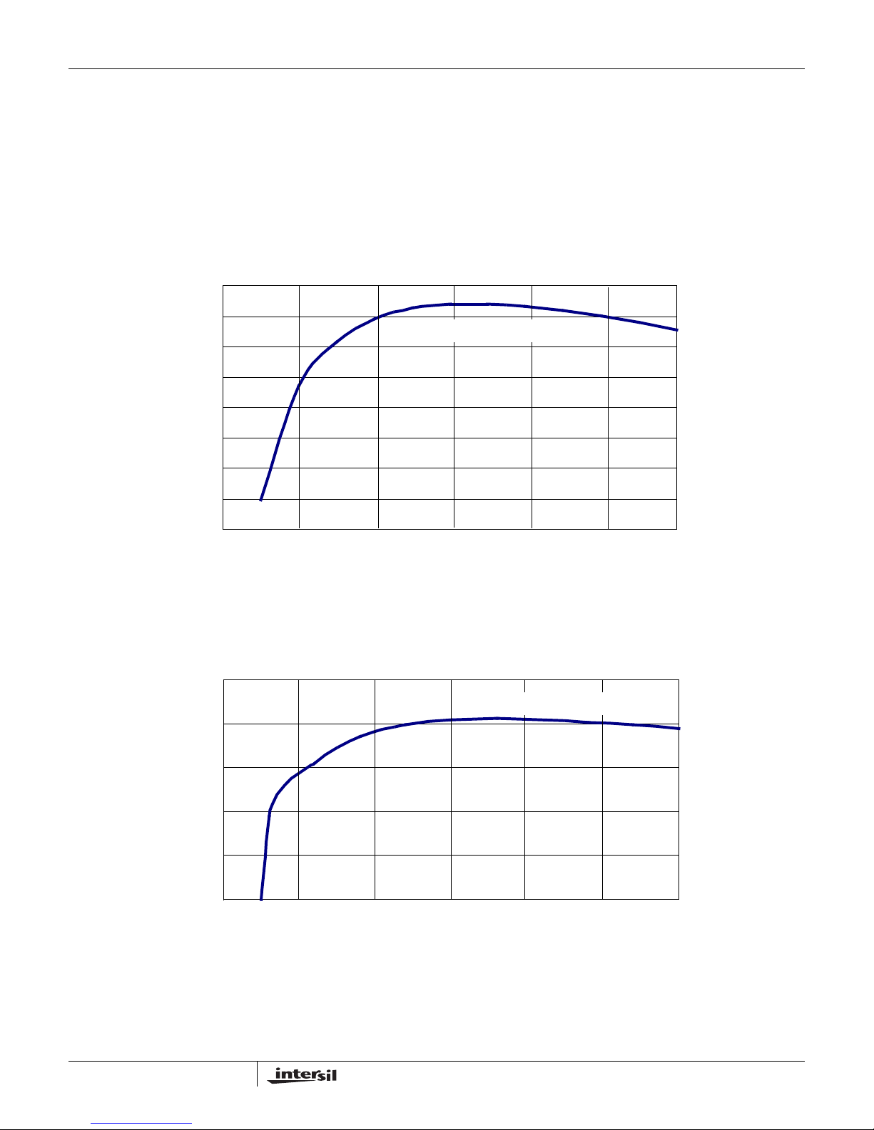
Efficiency
The measured input power includes the quiescent current
for all three controllers on the evaluation board and is
included in the efficiency measurement for the separate
channels. Adaptive diode emulation and adaptive
frequency modes are disabled for these efficiency
measurements.
92
90
88
86
84
82
EFFICIENCY (%)
80
CH 1, V
= 12V, V
IN
OUT
= 1.8V
78
76
OUTPUT CURRENT (A)
30 40 50 6020100
FIGURE 18. CHANNEL 1 EFFICIENCY
95
CH 2, VIN = 12V, V
90
85
80
EFFICIENCY (%)
75
70
0 5 10 15 20 25 30
OUTPUT CURRENT (A)
OUT
= 1.5V
28
FIGURE 19. CHANNEL 2 EFFICIENCY
September 11, 2009
AN1507.0
Page 29

Application Note 1507
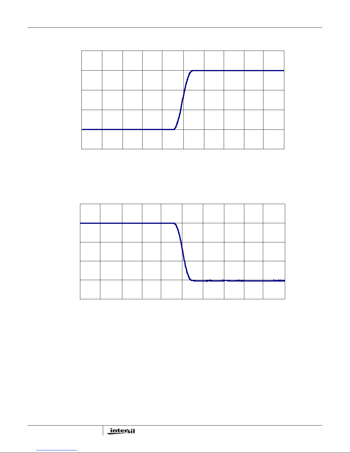
Ramp-up/Ramp-down Characteristics
2.0
1.5
1.0
0.5
OUTPUT VOLTAGE (V)
0
-0.5
0 0.01 0.02 0.03 0.04 0.05 0.06 0.07 0.08 0.09 0.10
TIME (s)
FIGURE 20. CHANNEL 1 RAMP UP
2.0
1.5
1.0
0.5
OUTPUT VOLTAGE (V)
0
-0.5
0 0.01 0.02 0.03 0.04 0.05 0.06 0.07 0.08 0.09 0.10
TIME (s)
FIGURE 21. CHANNEL 1 RAMP DOWN
29
September 11, 2009
AN1507.0
Page 30
Application Note 1507
Ramp-up/Ramp-down Characteristics (Continued)
2.0
1.5
1.0
0.5
OUTPUT VOLTAGE (V)
0
-0.5
0 0.01 0.02 0.03 0.04 0.05 0.06 0.07 0.08 0.09 0.1
TIME (s)
FIGURE 22. CHANNEL 2 RAMP UP
2.0
1.5
1.0
0.5
OUTPUT VOLTAGE (V)
0
-0.5
0 0.01 0.02 0.03 0.04 0.05 0.06 0.07 0.08 0.09 0.1
TIME (s)
FIGURE 23. CHANNEL 2 RAMP DOWN
30
September 11, 2009
AN1507.0
Page 31

Dynamic Load Response
0.005
0
-0.005
-0.010
-0.015
(V)
OUT
-0.020
V
-0.025
-0.030
-0.035
-0.040
0 0.05 0.10 0.15 0.20 0.25 0.30 0.35
FIGURE 24. CHANNEL 1 DYNAMIC RESPONSE, 30A TO 42A LOAD STEP
Application Note 1507
TIME (s)
(V)
OUT
V
-0.005
-0.010
0.030
0.025
0.020
0.015
0.010
0.005
0
0 0.05 0.10 0.15 0.20 0 .25 0.30 0.35
TIME (s)
FIGURE 25. CHANNEL 1 DYNAMCI RESPONSE, 42A TO 30A LOAD STEP
31
September 11, 2009
AN1507.0
Page 32

Application Note 1507
Dynamic Load Response (Continued)
0.015
0.010
0.005
0
-0.005
(V)
-0.010
OUT
V
-0.015
-0.020
-0.025
-0.030
-0.035
0 0.02 0.04 0.06 0.08 0.10 0.12 0.14 0.16 0.18 0 .20
FIGURE 26. CHANNEL 2 DYNAMIC RESPONSE, 21A TO 15A LOAD STEP
TIME (s)
0.030
0.025
0.020
0.015
0.010
0.005
(V)
OUT
V
-0.005
-0.010
-0.015
-0.020
-0.025
0
0 0.02 0.04 0.06 0.08 0.10 0.12 0.14 0.16 0.18 0.20
TIME (s)
FIGURE 27. CHANNEL 2 DYNAMIC RESPONSE, 15A TO 21A LOAD STEP
32
September 11, 2009
AN1507.0
Page 33

Application Note 1507
ORDERABLE
PART NUMBER DESCRIPTION
ZL6100EVAL2Z ZL6100 Two Channel Evaluation Kit (EVB, USB Adapter, Cable, Software)
References
12.ZL6100 Data Sheet, Intersil Corporation, 2009.
13.AN2033 – PMBus
Corporation, 2009.
™
Command Set, Intersil
Intersil Corporation reserves the right to make changes in circuit design, software and/or specifications at any time without notice. Accordingly, the
reader is cautioned to verify that the Applica tio n No te or Tec hnical Brief is current before proceeding.
For information regarding Intersil Corporation and its products, see www.intersil.com
33
September 11, 2009
AN1507.0
 Loading...