

Page 1
Description
The ZL2005P is an innovative mixed-signal
power management and conversion IC that
combines a compact, efficient, synchronous buck
controller, adaptive drivers and key power and
thermal management functions in a single
package. The ZL2005PEV4 platform allows
evaluation of the features in the highlyconfigurable ZL2005P via the SMBus interface
using PMBus™ commands. The PMBus
command set is accessed by using Zilker Labs
evaluation software from a PC running Microsoft
Windows.
This evaluation board is meant to enable rapid
evaluation of the functionality of the ZL2005P in
a 10 Amp configuration. It has been optimized for
ease of evaluation across a wide range of input
and output conditions. This ZL2005PEV4
platform is provided as a reference design.
Features
• PMBus control via SMBus
• Pin-strap selection for stand-alone operation
• V
• R
settable from +0.8V to +3.3V
OUT
sensing
DS(ON)
• Convenient power connection
• Onboard enable switch
• Power good indicator
• External temperature sensor
Target Specifications
This board has been designed for the following
conditions:
• V
• V
• I
• F
• Output ripple: < 1%
• Dynamic response 3% (7.5A - 10A step load) @ 2.5V
• Temperature: 25°C
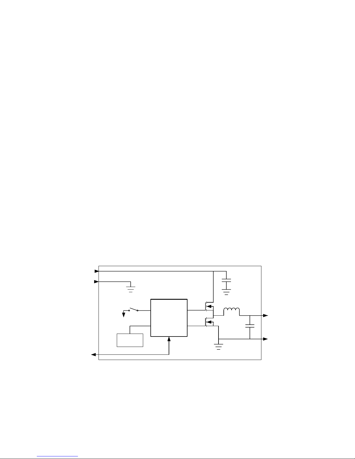
= 12V (Board range 4.5V to 13.2V)
IN
= 1.2V (Board range is 0.8V to 3.3V)
OUT
= 0A - 10A
OUT
= 600kHz
SW
POWER IN
EN
ZL2005P
POWER OUT
Address
select
SMBus
Figure 1. Block Diagram
Page 2

ZL2005PEV4
Functional Description
The ZL2005PEV4 provides the circuit required
to demonstrate the features of the ZL2005P in a
10Amp configuration. The ZL2005PEV4 has a
functionally-optimized layout that allows highlyefficient operation to its maximum output current
(See board picture in Figure 2). The input power
connection is provided through banana jack
terminals. Stand-alone operation of the ZL2005P
is achieved by factory installed pin-strap settings
and pre-configuration via PMBus commands.
PMBus protocol communication is performed
via a SMBus interface using an external USB to
SMBus adaptor. PMBus commands can be used
to modify the settings of the evaluation platform.
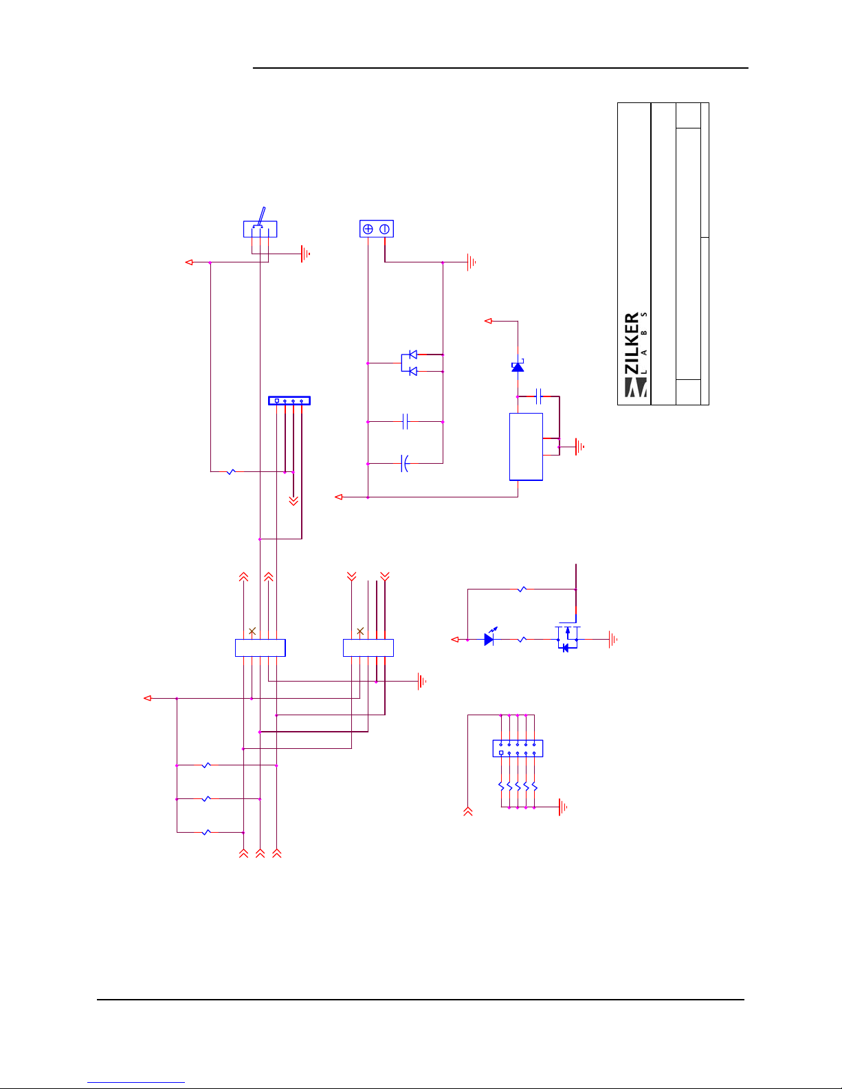
Figure 3 shows the ZL2005P circuit schematic.
The circuit consists of the ZL2005P power
conversion and management IC with its minimal
component count.
The input voltage connection is made at J1 which
is labeled VIN+/-. J2 is the output connector for
the output voltage, VOUT+/-. The VIN+/- and
VOUT+/- connections are rated to 10 A.
The ZL2005P SMBus address is set by the
jumper applied to J12. The SA1 pin is strapped
by an 11k resistor to ground. The J12 jumper
applies a different resistor to the SA0 pin to
achieve the indicated SMBus address settings.
Note that power must be cycled to set a new
address.
Refer to Figures 5 through 10 for component
placement and board layout. The board layout
has been optimized for two-sided component
area and thermal performance. For ZL2005P
circuit layout design considerations refer to
Zilker Labs Application Note AN10 (Reference
1 on page 21).
Figure 4 shows the ZL2005PEV4 interface
schematic. It contains various circuits that
interface to the ZL2005P’s circuit. The hardware
enable function is controlled by a toggle switch
(SW1) on the ZL2005PEV4 board. External
temperature is monitored from a 2N3904
transistor (Q3) connected to the XTEMP pin.
This external temperature is read with the
READ_TEMPERATURE_2 PMBus command.
The power good status is indicated by the PG
LED at D11. The PG LED indicates the correct
state of the power good signal when power is
applied to the ZL2005PEV4 board. The right
angle headers at opposite ends of the board (J10
and J11) are available to daisy chain multiple
boards. The SMBus and Enable signals are
passed between these connectors. All header pins
and switch positions are labeled on the
ZL2005PEV4 board’s silkscreen as shown in
Figure 5.
2 ZL2005PEV4DSr1.0
Page 3

ZL2005PEV4
Operation
Stand-Alone Operation
The ZL2005PEV4 is easy to setup and operate. It
is configured, out of the box, to provide 1.2V at
10A from a 12V source. All input and output
connections should be made before turning the
input supply on.
When the input power supply is turned on, and
the enable switch is set to enable, the ZL2005P
will output the configured voltage. A load can
be applied to the output and the circuit can be
tested.
PMBus Operation
The ZL2005P utilizes the PMBus protocol. The
PMBus functionality can be accessed via USB
from a PC running the Zilker Labs Evaluation
software on a Windows-XP or Windows2000/NT operating system.
The enable switch can then be moved to
“ENABLE” and the ZL2005P can be tested.
Alternatively, the PMBus commands
ON_OFF_CONFIG and OPERATION may be
used to manipulate the enable state.
Modifying the ZL2005PEV4
In order to design and test an alternative power
train circuit with the ZL2005P, choose a desired
operating conditions and power train. Enter the
selected power design parameters into Zilker
Labs’ PID calculation/simulation tool. The
results from the simulation tool provide
appropriate compensation values to configure the
new ZL2005P circuit. Apply the new power
train circuit to the evaluation board. Power the
board and invoke the evaluation software. Then
configure the new PID coefficients using the
“PMBus: Basic” command page or loading a
configuration text file with the new
compensation coefficients in it.
Install the Zilker Labs Evaluation software using
the CD included in the ZL2005PEV4 kit or
download it from the web at
www.zilkerlabs.com
For PMBus operation, connect a USB/SMBus
adaptor (J2) to the EVB (J10). Apply a USB
cable between the USB/SMBus adaptor and the
PC. Connect the output of the ZL2005PEV4 to
the desired load. Then connect an appropriate
power supply to the input. Place the enable
switch in “DISABLE” and turn on the power.
Invoke the ZL2005P interface software.
The Zilker Labs Evaluation software allows
modification of all ZL2005P PMBus parameters.
Manually configure the ZL2005P with the
interface software or load a predefined
configuration from a configuration text file.
Use the mouse-over pop-ups for help with the
Zilker Labs Evaluation software. Refer to the
Zilker Labs Application Note AN13 (Reference
3 on page 21) for PMBus details.
.
ZL2005PEV4DSr1.0 3
Page 4

ZL2005PEV4
Quick Start Guide
Stand-alone Operation
1. Set enable switch (EN) to “DISABLE”
2. Apply load to VOUT+/VOUT-
3. Connect power supply to VIN+/VIN-
(supply turned off)
4. Turn power supply on
5. Set enable switch (EN) to “ENABLE”
6. Test ZL2005P operation
PMBus Operation
1. Insert the Zilker Labs Eval Software CD
2. Install the Eval Software by running
setup.exe from the ZL_Eval_Installer folder
on the CD.
3. Connect a USB/SMBus adaptor (J2) to the
EVB (J10)
4. Select a SMBus address with the jumper on
J12
5. Connect supplied USB cable from computer
to EVB
a. Upon first time connection, the Found
New Hardware Wizard will appear.
Select “No, Not this time” and click
Next
b. Select “Install from a list or specific
location (Advanced)” and click Next
c. Select “Search the best driver in these
locations” and only select the “Search
removable media” option, then click
Next
d. If you encounter a popup warning during
driver installation, click the “Continue
Anyway” button
6. Follow steps 1 - 4 under Stand-alone
Operation
7. Invoke “Zilker_Labs_Eval” from the Start
menu under Zilker Labs
8. Monitor and configure EVB using the
informative pages in the evaluation software
9. Test the ZL2005P operation
Connect input
voltage here
Connect load
here
Connect SMBus
controller here
Connect other
eval boards here
PG LED EN Switch Address select
Figure 2. ZL2005PEV4 Evaluation Board
4 ZL2005PEV4DSr1.0
Page 5

ZL2005PEV4
Schematics
VOUT
VOUT
J2
VIN
C2
22uF
C1
22uF
L1
BSZ130
0.47uH
1
2
3
4
Q1
8
7
6
5
CON2_Banana
C10
47uF
VOUT
8
7
6
5
6.3V
47uF
6.3V
C9
C8
47uF
6.3V
C7
47uF
6.3V
C6
47uF
6.3V
Q2
BSZ035
GND
1
2
3
4
AUSTIN, TEXAS 78746
BUILD I NG A, SUI TE 100
4301 WESTBANK DRIVE
ZILKER L ABS, INC. CONFIDENTIAL AND PROPRIETARY
Title
of
12Tuesday , October 23, 2007
Sheet
RSCH-ZL2005-016 2.1
SCHEMATIC, 10A POIN T OF LOAD
A
Size Document Number Rev
Temperature Measurement
VIN
C5
1uF
ISENB
ISENA
GL
SW
GH
Optiona l
0
R1
C11
0.1uF
VDD
C3
4.7uF
V25
Q3
2N3904
28
29
30
31
32
33
34
35
36
BST
D1
BAT54
C12
0.1uF
C4
4.7uF
24
25
GH
SW
20
21
23
22
GL
VR
PGND
SGND
ISENB19ISENA
VSEN
VTRK
SS1
SS0
UVLO
V1
V0
FC1
ZL2005P
FC0
26
27
BST
VDD
V25
XTEMP
VADJ
MGN
CFG
EN
DLY0
DLY1
PG
VSENSE
GND_SIGNAL
GND_SIGNAL
37
18
17
16
15
R5
14
13
12
11
10
34.8k
VO UT max set
R4
16.2k
to 3.3V
place near low side FET
DGND1SYNC2SA03SA14ILIM16SCL7SDA8SALRT
U1
ILIM0
9
5
R3
11k
SMBus Address
set by J12
(page 2)
PG
EN
ZL2005PEV4DSr1.0 5
SYNC
SA0
SCL
SDA
SALRT
VTRK
Figure 3. ZL2005P Circuit
Page 6
ZL2005PEV4
of
Enable
Monitor
Di sable
SW1
123
SW_SPDT
+Vi2c
Enable on PG_0
Enable Open
Enable on Bus
JP1
213
4
R13
10.0K
SYNC
VTRK
VIN
EN
VIN
J1
VOUT
CON2_Banana
AUSTIN, TEXAS 78746
BUILD ING A, SU I TE 100
4301 WESTBANK DRIVE
+Vi2c
D10
STPS20L45CG
D-2PAK
Backside
C67
22uF
C63
180uF
16V
PG
This regulator allows stand alone operation when not
using a USB dongle. When no USB dongle is applied,
this regualtor is supplying Vi2c current thus
efficiency measurements will be affected.
D12
BAT54
U10
C68
22uF
3
VO
G
4
G
2
VI
MIC2920A-3.3BS
1
R15
10.0K
ZILKER LABS, INC. CONFIDENTIAL AND PROPRIETARY
PG
SCHEMATIC, Interface
Title
22Tuesday , June 12, 2007
Sheet
RSCH-ZL2005-016 2
A
Size Docum ent Number Rev
SYNC
To Next Rail
J11
EN_BUS
13579
246
8
R14
470
+Vi2c
D11
SA0
GRN
21
J12
3 4
5 6
R1719.6k
R1821.5k
R1923.7k
Addr
0x20
0x21
Q10
2N7002/SOT
The referenc e des igns c ont ained in this doc um ent are f or reference and exam ple purpos e only .
THE REFERENCE D ESI GN S AR E PR OVIDED "AS IS" AN D "W I TH ALL F AU LTS" AND ZILKER
LABS DISC LAMES ALL WAR R AN TIES, WH ETHER D I R EC T, I ND I R EC T, C ON SEQU EN TIAL
(INCLUDING LOSS OF PROFITS), OR OTHERWISE, RESU LTING FROM THE R EFERENCE
DESIGN S O R AN Y USE THER EOF .
Any us e of such ref erenc e des igns is at y our own risk and y ou agree to indem nif y Z ilk er Labs
f or any dam ages res ult ing f rom s uc h us e.
7 8
9 10
HEADER 5x 2 PI N
R2026.1k
R2128.7k
0x22
0x23
0x24
HEADER 5X2
10
+Vi2c
Place pullups near J11
EN_BUS
PG_0
13579
J10
From Previous Rail
246
8
HEADER 5X2
10
R12
10.0K
R11
10.0K
R10
10.0K
SDA
SALRT
SCL
SCL
SDA
SALRT
Figure 4. ZL2005P Interface
6 ZL2005PEV4DSr1.0
Page 7

ZL2005PEV4
Board Layout
ZL2005PEV4DSr1.0 7
Figure 5. PCB – Silk Screen Top
Page 8

ZL2005PEV4
8 ZL2005PEV4DSr1.0
Figure 6. PCB – Top Layer
Page 9

ZL2005PEV4
ZL2005PEV4DSr1.0 9
Figure 7. PCB – Inner Layer 1
Page 10

ZL2005PEV4
10 ZL2005PEV4DSr1.0
Figure 8. PCB – Inner Layer 2
Page 11

ZL2005PEV4
ZL2005PEV4DSr1.0 11
Figure 9. PCB – Bottom Layer (Top view)
Page 12

ZL2005PEV4
Figure 10. PCB – Silk Screen Bottom (Top View - reversed)
12 ZL2005PEV4DSr1.0
Page 13

ZL2005PEV4
C
S
Bill Of Materials
Item Quan Reference Value Tolerance Rating Type PCB Footprint Manufacturer Part Number
1 4 C1 ,C2,C67,C68 22uF 16V X5R SM1210 MURATA GRM32ER 61C226K E20L
2 2 C3,C4 4.7uF 6.3V X5R SM0603 Panasonic - ECG ECJ-1VB0J475M
3 1 C5 1uF 25V X5R SM0603 TAIYO YUDEN TMK107BJ105KA-T
4 5 C6,C7,C8,C9,C10 47uF 20% 6.3V X5R SM1206_A_REV1 TDK C3216X5R0J476M
5 2 C1 1,C12 0.1uF 10% 50V X7R SM0603 MURA TA GRM39X7R104K0 50AD
6 1 C63 180uF 16V ELECT POLY SM_CAP_8.3X8.3_PXA United Chemi-Con APXA160ARA181MHC0G
7 2 D1,D12 BAT54 30V Schottky SOD523 ON Semiconductor BAT54XV2T1OS
8 1 D10 STPS20L45CG D-2PAK STMicro STPS20L45CG
9 1 D11 GRN 2V led2-45x51 CHICAGO MINIATURE CMD17-21VGC
10 1 JP1 4 PIN SIP4/100 SAMTEC TSW-104-07-T-S
11 2 J1,J2 CON2_Banana JACK_F_NI_2P.750SP_.175PLUG Emerson 108-0740-001
12 1 J10 HEADER 5X2 HDR10DUAL100X100 SAMTEC TSW-105-08-T-D-RA
13 1 J11 HEADER 5X2 HDRF5DUALRA100X100 SAMTEC SSQ-105-02-T-D-RA
14 1 J12 HEADER 5x2 PIN HDR10DUAL100X100 SAMTE
15 1 L1 0.47uH 17.5A Powder IHLP_2525BD_RE V1 Vishay IHLP2525C ZERR 47M 01
16 1 Q1 BSZ130 PP1212SP INFINEON BSZ130N03LS
17 1 Q2 BSZ035 PP1212SP INFINEON BSZ035N03LS
18 1 Q3 2N3904 40V NPN SOT-23 ON SEMI MMBT3904LT3
19 1 Q10 2N7002/SOT 60V N-CH SOT-23 ON SEMI 2N7002LT1
20 1 R1 0 SM0603 PANASONIC-ECG ERJ-3GEY0R00V
21 1 R3 11k 1% SM0402
22 1 R4 16.2k 1% SM0402
23 1 R5 34.8k 1% SM0402
24 5 R10,R11,R12,R13,R15 10.0K 1% SM0402 VENKEL CR0402-16W-1002FT
25 1 R14 470 1% SM0402 Rohm MCR01MZPF4700
26 1 R17 19.6k 1% SM0402 VISHAY
27 1 R18 21.5k 1% SM0402 VISHAY
28 1 R19 23.7k 1% SM0402 VISHAY
29 1 R20 26.1k 1% SM0402 VENKEL CR0402-16W-2612FT
30 1 R21 28.7k 1% SM0402 VISHAY
31 1 SW1 SW_SPDT SW_TOG_ULTRAMIN_SPDT NKK
32 1 U1 ZL2005P MLF36 Zilker Labs ZL2005P
33 1 U10 MIC2920A-3.3BS SOT223_1234_FLD Micrel MIC2920A-3.3WS
34 1 PCB MPWB-ZL2005-016
35 2 J12-Addr22,JP1-ENbus CONN JUMPE R S H OR TING G OL D SULLIN
36 4 SCREW MACHINE P H IL L IP S 4-40 X 1 /4 BUIL D IN G FAS T E N ERS PMS 440 0025 P H
37 4 STANDOFF RD 4-40THR .750" ALUM KEYSTONE ELECTRONICS 3481
38 4 J1_2ea,J2_2ea CAP_MO LDE D.25ID_BLK CAP_MO LDED .25ID CAPLU GS VC-234-8
PANASONIC-ECG ERJ-2RKF1102X
PANASONIC-ECG ERJ-2RKF1622X
PANASONIC-ECG ERJ-2RKF3482X
TSW-105-07-T-D
CRCW040219K6FKED
CRCW040221K5FKED
CRCW040223K7FKED
CRCW040228K7FKED
G-13AP-RO
SSC02SYAN
Table 1. ZL2005PEV4 Rev. 2 Bill of Materials
ZL2005PEV4DSr1.0 13
Page 14

ZL2005PEV4
ZL2005P Characterization Data
The following data was acquired using a ZL2005PEV4 rev 2 evaluation board.
Test 1: Efficiency
Efficiency data was collected for several output voltages for input voltages of 5 V and 12 V. Note that this
data is for informational use only, as the board is optimized for 12 V input and 1.2 V output operation.
Effi ci ency VI N=5V
100
95
90
85
80
Eff in %
75
70
65
60
012345678910
IOUT (Amp)
Vout=1V Vout=1.2V Vout=1.5V Vout=1.8V Vout=2.5V Vout=3.3V
Figure 11. Efficiency Test, VIN = 12 V. fSW = 600 kHz
14 ZL2005PEV4DSr1.0
Page 15

ZL2005PEV4
Efficiency VIN =12V
100
95
90
85
80
Eff in %
75
70
65
60
012345678910
IOUT (Amp)
Vout=1V Vout=1.2V Vout=1.5V Vout=1.8V Vout=2.5V Vout=3.3V
Figure 12. Efficiency Test, VIN = 5 V, fSW = 600 kHz
ZL2005PEV4DSr1.0 15
Page 16

ZL2005PEV4
Test 2: Ramp-Up/Ramp-Down Characteristics
Ramp-up and ramp-down data was acquired based on a nominal output voltage of 1.5 V and a preset
ramp-up and ramp-down period of 10 ms.
R am p up 10ms
VOUT =1.5V
2
1.75
1.5
1.25
1
VOUT in V
0.75
0.5
0.25
0
0.0 10.0 20.0 30.0 40.0 50.0 60.0 70.0 80.0 90.0 100.0
Time in ms
VOUT in Volt
Figure 13. Ramp-Up Characteristic Test Results, Vin = 12 V, Vout = 1.5 V, Iout = 1 A
16 ZL2005PEV4DSr1.0
Page 17

ZL2005PEV4
R am p D ow n 10m s
VOUT =1.5V
2
1.75
1.5
1.25
1
VOUT in V
0.75
0.5
0.25
0
0.0 10.0 20.0 30.0 40.0 50.0 60.0 70.0 80.0 90.0 100.0
Time in ms
Ramp Down Amplitude (Volts)
Figure 14. Ramp-Down Characteristic Test Results, Vin = 12 V, Vout = 1.5 V, Iout = 1 A
ZL2005PEV4DSr1.0 17
Page 18

ZL2005PEV4
Test 3: Dynamic Load Response
For the dynamic load response test, the circuit was set to a nominal output voltage of 2.5 V and an input
voltage of 6 V. A 7.5 A to 10 A load step (rate of 2.5 A/µs) was applied and then released, and the
deviation from nominal output was captured in the charts below.
Transient L to H
0.03
0.02
0.01
0
-0.01
-0.02
Vout in Volt
-0.03
-0.04
-0.05
-0.06
0.0E+00 5.0E-05 1.0E-04 1.5E-04 2.0E-04 2.5E-04 3.0E-04 3.5E-04 4.0E-04
Time in Sec
Dyn am ic Load Respon se ( Volt s)
Figure 15. Dynamic Load Test Results
Transi ent H t o L
0.06
0.05
0.04
0.03
0.02
0.01
0
-0.01
Vout in Volt
-0.02
-0.03
-0.04
-0.05
0.0E+00 5.0E-05 1.0E-04 1.5E-04 2.0E-04 2.5E-04 3.0E-04 3.5E-04 4.0E-04
Time in Sec
VOUT in V
18 ZL2005PEV4DSr1.0
Figure 16. Dynamic Unload Test Results
Page 19

ZL2005PEV4
Default Configuration Text
The following PMBus commands have been loaded and stored into the Default Store of the ZL2005P
device. Each PMBus can be accessed with the Zilker Labs Evaluation software. The # symbol is used for
a comment line.
# Configuration file for ZL2005PEV4, Rev 2
#syntax:
#PMBus Command <tab> Value
#Erase default and user store
RESTORE_FACTORY
STORE_DEFAULT_ALL
MFR_ID ZilkerLabs
MFR_MODEL ZL2005PEV4
MFR_REVISION Rev_1.4
MFR_LOCATION Austin_TX
VIN_OV_FAULT_LIMIT 13.5
VIN_OV_WARN_LIMIT 13.2
VIN_UV_FAULT_LIMIT 4.2
VIN_UV_WARN_LIMIT 4.5
VOUT_COMMAND 1.2 #V
FREQUENCY_SWITCH 600 #kHz
POWER_GOOD_DELAY 1
TON_DELAY 15
TON_RISE 5
TOFF_DELAY 15
TOFF_FALL 5
SEQUENCE 0x0000
#Use Rdson current sense method with internal temp sensor
MFR_CONFIG 0x7981
USER_CONFIG 0x0000
PID_TAPS A=4163.75, B=-7518.75, C=3513.44
IOUT_OC_FAULT_LIMIT 20.
IOUT_AVG_OC_FAULT_LIMIT 15.
IOUT_UC_FAULT_LIMIT -10.
IOUT_AVG_UC_FAULT_LIMIT -8.
#low FET not enabled for output OV, output OV and UV count to 2
OVUV_CONFIG 0x01
ZL2005PEV4DSr1.0 19
Page 20

ZL2005PEV4
IOUT_SCALE 3.65
IOUT_CAL_OFFSET -0.7
#Set temperature compensation at 4000ppm/ C internal temp sensor
TEMPCO_CONFIG 0x28
#NLR_CONFIG Enable,2.5%,No Outer,3.0%,1,7,0
NLR_CONFIG 0xc530
#VOUT_DROOP 2 #mV/A
STORE_DEFAULT_ALL
RESTORE_DEFAULT_ALL
20 ZL2005PEV4DSr1.0
Page 21

ZL2005PEV4
References
[1] AN10 – ZL2005 Thermal and Layout
Guidelines for the ZL2005, Zilker Labs,
Inc., 2007.
[2] ZL2005P Data Sheet, Zilker Labs, Inc.,
2007.
™
[3] AN13 – ZL2005 and PMBus
Labs, Inc., 2007.
Revision History
, Zilker
Date Rev.
#
1-29-2008 1.0 Initial Release
ZL2005PEV4DSr1.0 21
Page 22

ZL2005PEV4
Zilker Labs, Inc.
4301 Westbank Drive
Building A-100
Austin, TX 78746
Tel: 512-382-8300
Fax: 512-382-8329
www.zilkerlabs.com
© 2008, Zilker Labs, Inc. All rights reserved. Zilke r Labs, Digital-DC and the Zilker Lab s Logo are trademarks
of Zilker Labs, Inc. All other products or brand names mentioned herein are trademarks of their respective holders.
Pricing, specifications and availability are subject to change without notice. Please see www.zilkerlabs.com for
updated information. This product is not intended for use in connection with any high-risk activity, including
without limitation, air travel, life critical medical operations, nuclear facilities or equipment, or the like.
The reference designs contained in this document are for reference and example purposes only. THE REFERENCE DESIGNS ARE PROVIDED "AS IS" AND "WITH ALL FAULTS" AND ZILKER LABS DISCLAIMS
ALL WARRANTIES, WHETHER EXPRESS OR IMPLIED. ZILKER LABS SHALL NOT BE LIABLE FOR
ANY DAMAGES, WHETHER DIRECT, INDIRECT, CONSEQUENTIAL (INCLUDING LOSS OF PROFITS), OR OTHERWISE, RESULTING FROM THE REFERENCE DESIGNS OR ANY USE THEREOF. Any
use of such reference designs is at your own risk and you agree to indemnify Zilker Labs for any damages resulting from such use.
22 ZL2005PEV4DSr1.0
 Loading...