Synchronous Step-Down MOSFET Drivers
ZL1505
ZL1505
The ZL1505 is an integrated high-speed, high-current
N-channel MOSFET driver for synchronous step-down
DC-DC conversion applications. When used with Zilker
Labs Digital-DC™ PWM controllers, the ZL1505 enables
dynamically adaptive dead-time control that optimizes
efficiency under all operating conditions. A dual input
PWM configuration enables this efficiency optimization
while minimizing complexity within the driver.
Operating from a 4.5V to 7.5V input, the ZL1505
combines a 5A, 0.5W low-side driver and a 3A, 0.8W
high-side driver to support high step-down buck
applications. A unique adjustable gate drive current
scheme allows the user to adjust the drive current on
both drivers to optimize performance for a wide rage of
input/output voltages, load currents, power MOSFET s
and switching frequencies up to 1.4MHz. An integrated
30V bootstrap Schottky diode is used to charge the
external bootstrap capacitor. An internal w atchdog circuit
prevents excessive shoot-through currents and protects
the external MOSFET switches.
The ZL1505 is specified over a wide -40°C to +125°C
junction temperature range and is available in an
exposed pad DFN-10 package.
Features
• High-speed, high-current drivers for synchronous
N-channel MOSFETs
• Adaptive dead-time control optimizes efficiency
when used with Digital-DC controllers
• Integrated 30V bootstrap Schottky diode
• Capable of driving 40A per phase
• Supports switching frequency up to 1.4MHz
- >4A source, >5A sink low-side driver
- >3A source/sink high-side driver
- <10ns rise/fall times, low propagation delay
• Adjustable gate drive strength optimizes efficiency
, V
, I
for different V
combinations
• Internal non-overlap watchdog prevents
shoot-through currents
IN
OUT
, FSW and MOSFET
OUT
Applications*(see page 12)
• High efficiency, high-current DC/DC buck converters
with digital control and PMBus™
• Multi-phase digital DC/DC converters with phase
adding/dropping
•Power train modules
• Synchronous rectification for secondary side isolated
power converters
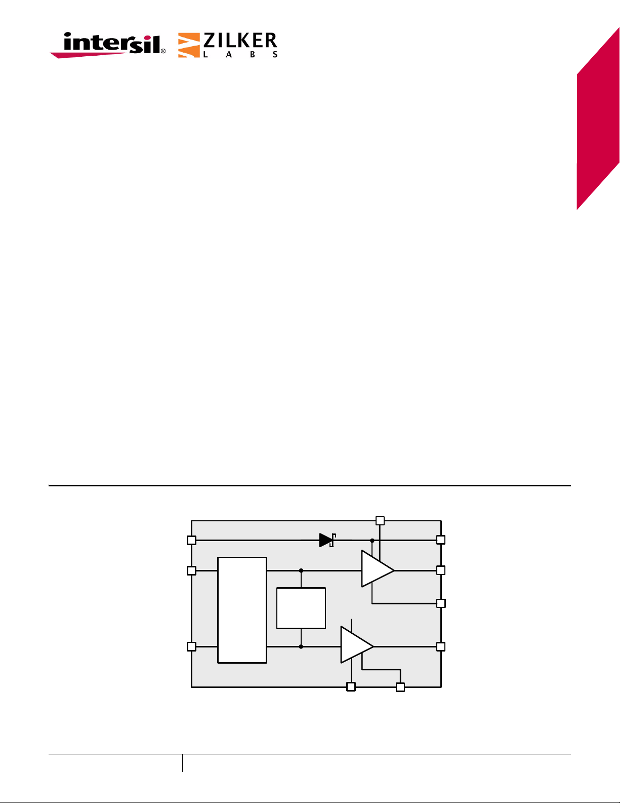
VDD
PWMH
PWML
Related Literature*(see page 12)
• FN6846 ZL2004 Data Sheet
HSEL
Level
shift
Shoot-
through
Protection
VDD
ZL1505
GND
FIGURE 1. ZL1505 BLOCK DIAGRAM
BST
GH
SW
GL
LSEL
December 4, 2009
FN6845.1
1
CAUTION: These devices are sensitive to electrostatic discharge; follow proper IC Handling Procedures.
1-888-INTERSIL or 1-888-468-3774
| Intersil (and design) is a registered trademark of Intersil Amer ic as Inc .
All other trademarks mentioned are the property of their respective owners.
Copyright Intersil Americas Inc. 2009. All Rights Reserved

ZL1505
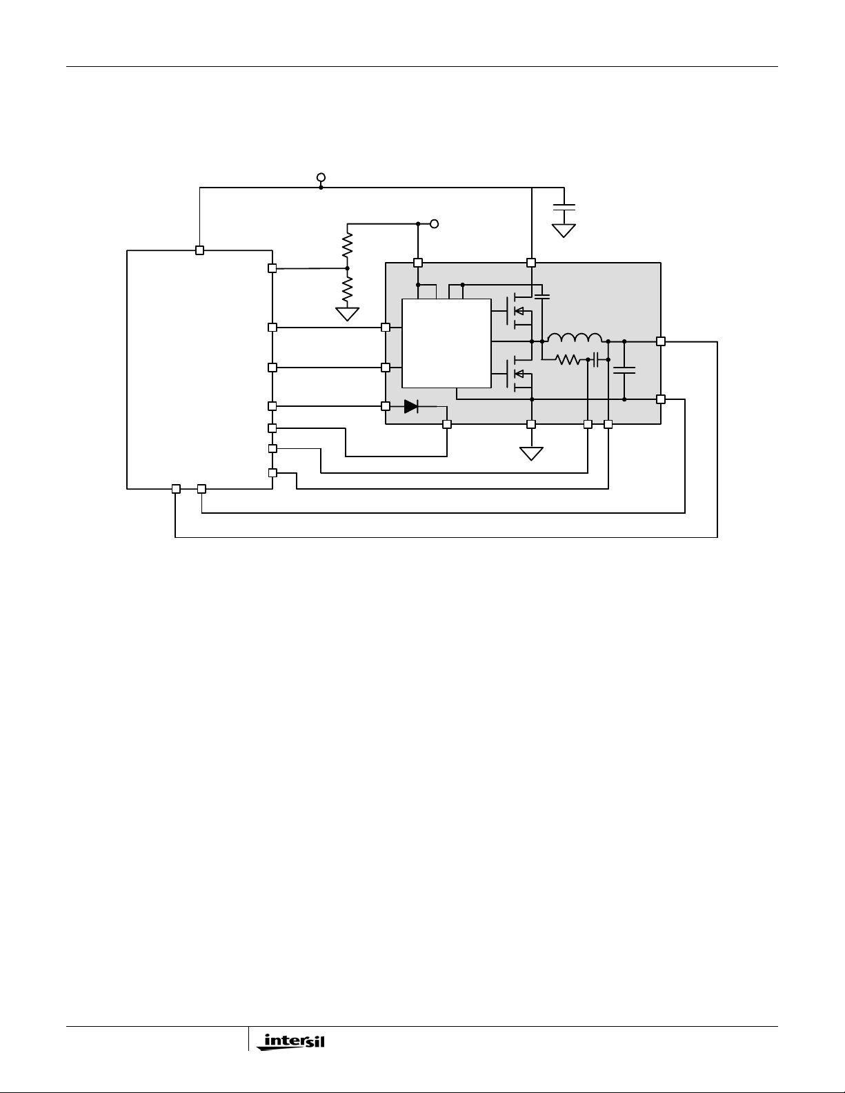
Typical Application Circuit
The following application circuit represents the typical implementation of the ZL1505 (Notes 1, 2).
V
IN
4.5-14V
V
BIAS
4.5-7.5V
VMON
VIN
PWMH
PWMH
PWMH
ZL2004
PWML
XTEMP
VSEN+
SGND
VSEN-
PWML
TEMP+
ISENA
ISENB
FIGURE 2. POWER TRAIN MODULE USING ZL2004 PWM CONTROLLER
NOTES:
1. For V
specified in Figure 2.
2. V
of 4.5V to 7.5V, the maximum VIN of the ZL1505 is 22.5V to 25.5V. ZL1505 input supply voltage range (VIN) is
DD
for this application circuit is limited by the ZL2004 VIN of 4.5V to 14V.
IN
PWML
TEMP-
VDD
HSEL
LSEL
ZL1505
VINVDD
Power Train
Module
GH
BST
SW
GL
GND
GND
CS-CS+
VOUT
GND
2
FN6845.1
December 4, 2009

Pin Configuration
ZL1505
ZL1505
(10 LD DFN)
TOP VIEW
HSEL
GH
SW
PWMH
PWML
1
2
*EPAD
3
4
5
*CONNECT TO GND
BST
10
VDD
9
GL
8
7
GND
LSEL
6
Pin Descriptions
PIN NUMBER PIN NAME TYPE (Note 3) DESCRIPTION
1 HSEL I High-side gate drive current selector. Connect to BST for maximum gate
drive current; Connect to SW for 50% of maximum gate drive current.
2 GH O Output of high-side gate driver. Connect to the gate of high-side FET.
3 SW I/O Phase node. Return path for high-side driver. Connect to source of high-side
4 PWMH I High-side PWM control input.
5 PWML I Low-side PWM control input.
6 LSEL I Low-side gate drive current selector. Connect to VDD for maximum gate
FET and drain of low-side FET.
drive current; Connect to GND for 50% of maximum gate drive current.
7 GND PWR Ground. All signals return to this pin.
8 GL O Output of low-side gate driver. Connect to the gate of low-side FET.
9 VDD PWR Gate drive bias supply . Connect a high quality bypass capacitor from this pin
to GND.
10 BST PWR Bootstrap supply. Connect external capacitor to SW node.
ePad GND PWR Ground.
NOTE:
3. I = Input, O = Output, PWR = Power OR Ground.
Ordering Information
PACKAGE
PART NUMBER
(Notes 4, 5, 6)
PART
MARKING
TEMP RANGE
(°C)
Tape and Reel
(Pb-free)
ZL1505ALNNT 1505 -40 to +125 10 Ld 3x3 DFN L10.3x3D
ZL1505ALNNT1 1505 -40 to +125 10 Ld 3x3 DFN L10.3x3D
NOTES:
4. Please refer to TB347
for details on reel specifications.
5. These Intersil Pb-free plastic packaged products employ special Pb-free material sets; molding compounds/die attach
materials and NiPdAu plate - e4 termination finish, which is RoHS compliant and compatible with both SnPb and Pb-free
soldering operations. Intersil Pb-free products are MSL classified at Pb-free peak reflow temperatures that meet or exceed
the Pb-free requirements of IPC/JEDEC J STD-020.
6. For Moisture Sensitivity Level (MSL), please see device information page for ZL1505
techbrief TB363
.
. For more information on MSL please see
PKG.
DWG. #
3
FN6845.1
December 4, 2009

ZL1505
Absolute Maximum Ratings Thermal Information
Voltage Measured with Respect to GND
DC Supply Voltage for VDD Pin . . . . . . . . . . . . .-0.3V to 8V
High-Side Supply Voltage for BST Pin . . . . . . . . -0.3V to 30V
High-Side Drive Voltage for
GH Pin . . . . . . . . . . . . . . . (V
Low-Side Drive Voltage for
GL Pin . . . . . . . . . . . . . . . .(GND - 0.3V) to (V
Boost to Switch Differential (V
BST, SW Pins . . . . . . . . . . . . . . . . . . . . . . . .-0.3V to 8V
SW
- VSW) for
BST
- 0.3V) to (V
BST
DD
+ 0.3V)
+ 0.3V)
Switch Voltage for SW Pin
Continuous . . . . . . . . . . . . . . . . . . . (GND - 0.3V) to 30V
<100ns . . . . . . . . . . . . . . . . . . . . . . .(GND - 5V) to 30V
Logic I/O Voltage for PWMH, PWML, LSEL Pins. . .-0.3V to 8V
HSEL Pin . . . . . . . . . . . . . (V
ESD Rating
- 0.3V) to (V
SW
BST
+ 0.3V)
Human Body Model . . . . . . . . . . . . . . . . . . . . . . . . . 2kV
GL Pin . . . . . . . . . . . . . . . . . . . . . . . . . . . . . . . . 1.5kV
Machine Model . . . . . . . . . . . . . . . . . . . . . . . . . . . 500V
Latch Up . . . . . . . . . . . . . . . . . . . . . . . . Tested to JESD78
CAUTION: Do not operate at or near the maximum ratings listed for extended periods of time. Exposure to such conditions may adversely impact
product reliability and result in failures not covered by warranty.
NOTES:
7. θJA is measured in free air with the component mounted on a high effective thermal conductivit y test board with “direct attach”
features. See Tech Brief TB379.
8. For θ
, the “case temp” location is the center of the exposed metal pad on the package underside.
JC
Thermal Resistance (Typical) θ
(°C/W) θJC (°C/W)
JA
10 Ld DFN (Notes 7, 8). . . . . . . . . 50 7
Junction Temperature Range . . . . . . . . . . -55°C to +150°C
Storage Temperature Range . . . . . . . . . . . -55°C to +150°C
Pb-Free Reflow Profile . . . . . . . . . . . . . . . . . .see link below
http://www.intersil.com/pbfree/Pb-FreeReflow.asp
Recommended Operating Conditions
Gate Drive Bias Supply Voltage Range
VDD . . . . . . . . . . . . . . . . . . . . . . . . . . . . . .4.5V to 7.5V
Input Supply Voltage Range, V
Operating Junction Temperature Range, TJ. . -40°C to +125°C
. . . . . . . . 3V to 30V - V
IN
DD
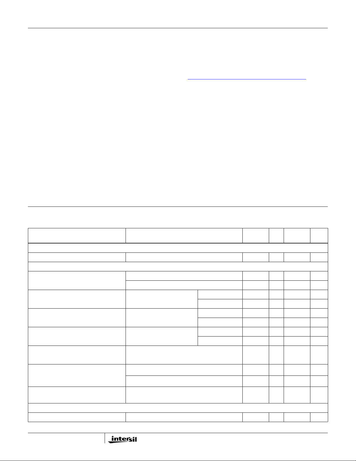
Electrical Specifications V
PARAMETER CONDITIONS
= 6.5V, TJ = -40°C to +125°C unless otherwise noted. Typica l values are at
DD
T
=+25°C. Boldface limits apply over the operating temperature range,
A
-40°C to +125°C.
MIN
(Note 9) TYP
MAX
(Note 9) UNIT
BIAS CURRENT CHARACTERISTICS
I
supply current Not switching – 110 180 µA
DD
PWM INPUT CHARACTERISTICS
PWM input bias current V
PWM input logic low, V
PWM input logic high, V
IL
IH
= 5 V –5–µA
PWM
V
= 0 V ––1µA
PWM
PWMH or PWML VDD = 6.5V 1.7 2 2.2 V
V
= 5.0 V 1.5 1.7 1.9 V
DD
PWMH or PWML VDD = 6.5V 2.8 3.1 3.4 V
VDD = 5.0V 2.2 2.5 2.7 V
Hysteresis PWMH or PWML V
Minimum PWMH On-time to Produce GH
Pulse, t
PWMH,ON
Minimum GH On-time pulse, t
(Note 11)
(Note 10)
GH,ON
= 0 – 8.5 12 ns
C
GH
CGH = 0 – 10 14 ns
C
GH
= 3 nF, V
HSEL
= V
BST
= 6.5V - 1.1 - V
DD
V
= 5.0V - 0.8 - V
DD
-1420 ns
Minimum PWMH Off-time to Produce
Valid GH Pulse, t
PWMH,OFF
BOOTSTRAP DIODE CHARACTERISTICS
Forward Voltage (V
) Forward bias current 100 mA – 0.8 – V
F
4
CGH = 0 – 13 17 ns
FN6845.1
December 4, 2009
 Loading...