®
www.BDTIC.com/Intersil
X9C102, X9C103, X9C104, X9C503
Data Sheet December 20, 2006
Digitally Controlled Potentiometer
(XDCP™)
FEATURES
• Solid-state potentiometer
• 3-wire serial interface
• 100 wiper tap points
—Wiper position stored in nonvolatile memory
and recalled on power-up
• 99 resistive elements
—Temperature compensated
—End to end resistance, ±20%
—Terminal voltages, ±5V
• Low power CMOS
= 5V
—V
CC
—Active current, 3mA max.
—Standby current, 750µA max.
• High reliability
—Endurance, 100,000 data changes per bit
—Register data retention, 100 years
• X9C102 = 1kΩ
• X9C103 = 10kΩ
• X9C503 = 50kΩ
• X9C104 = 100kΩ
• Packages
—8 Ld SOIC and 8 Ld PDIP
• Pb-free plus anneal available (RoHS compliant)
FN8222.1
DESCRIPTION
The X9Cxxx are Intersil digitally controlled (XDCP)
potentiometers. The device consists of a resistor
array, wiper switches, a control section, and nonvolatile memory. The wiper position is controlled by a
three-wire interface.
The potentiometer is implemented by a resistor array
composed of 99 resistive elements and a wiper switching network. Between each element and at either end
are tap points accessible to the wiper terminal. The
position of the wiper element is controlled by the CS
, and INC inputs. The position of the wiper can be
U/D
stored in nonvolatile memory and then be recalled
upon a subsequent power-up operation.
The device can be used as a three-terminal potentiometer or as a two-terminal variable resistor in a wide
variety of applications including:
– control
– parameter adjustments
– signal processing
,
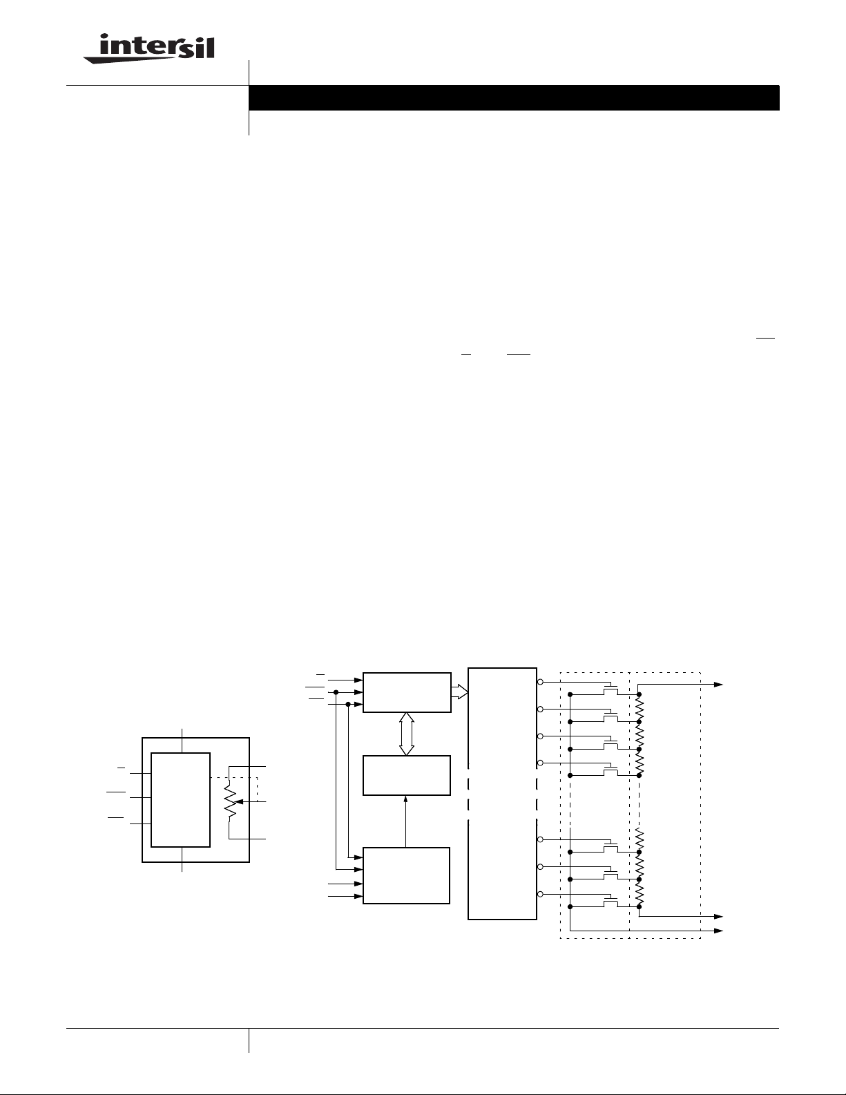
BLOCK DIAGRAM
7-Bit
Up/Down
Counter
7-Bit
Nonvolatile
Memory
Store and
Recall
Control
Circuitry
CAUTION: These devices are sensitive to electrostatic discharge; follow proper IC Handling Procedures.
1-888-INTERSIL or 1-888-468-3774
XDCP is a trademark of Intersil Americas Inc. Copyright Intersil Americas Inc. 2005, 2006. All Rights Reserved
99
98
97
96
One
of
OneHundred
Decoder
Detailed
| Intersil (and design) is a registered trademark of Intersil Americas Inc.
All other trademarks mentioned are the property of their respective owners.
Up/Down
Increment
Device
Select
(U/D
(INC
(CS
V
CC
)
)
)
(Supply Voltage)
Control
and
Memory
VSS (Ground)
General
U/D
INC
CS
VH/R
H
RW/V
W
VL/R
L
V
CC
GND
1
RH/V
H
Transfer
Gates
2
1
0
Resistor
Array
R
L/VL
RW/V
W

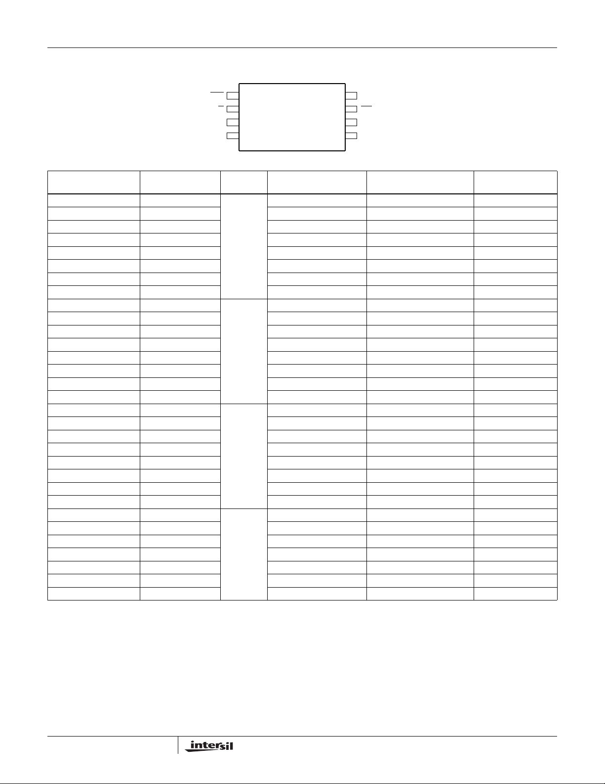
PIN CONFIGURATION
www.BDTIC.com/Intersil
X9C102, X9C103, X9C104, X9C503
DIP/SOIC
INC
U/D
VH/R
V
SS
1
2
X9C102/103/104/503
3
H
4
V
8
CC
CS
7
VL/R
6
5
VW/R
L
W
ORDERING INFORMATION
R
PART NUMBER PART MARKING
X9C102P X9C102P 1 0 to 70 8 Ld PDIP MDP0031
X9C102PZ (Note) X9C102P Z 0 to 70 8 Ld PDIP (Pb-free) MDP0031
X9C102PI X9C102P I -40 to 85 8 Ld PDIP MDP0031
X9C102PIZ (Note) X9C102P ZI -40 to 85 8 Ld PDIP (Pb-free) MDP0031
,
X9C102S*
X9C102SZ* (Note) X9C102S Z 0 to 70 8 Ld SOIC (Pb-free) MDP0027
X9C102SI*
X9C102SIZ*
X9C103P X9C103P 10 0 to 70 8 Ld PDIP MDP0031
X9C103PZ (Note) X9C103P Z 0 to 70 8 Ld PDIP (Pb-free) MDP0031
X9C103PI X9C103P I -40 to 85 8 Ld PDIP MDP0031
X9C103PIZ (Note) X9C103P ZI -40 to 85 8 Ld PDIP (Pb-free) MDP0031
X9C103S*
X9C103SZ*
X9C103SI*
X9C103SIZ*
X9C503P X9C503P 50 0 to 70 8 Ld PDIP MDP0031
X9C503PZ (Note) X9C503P Z 0 to 70 8 Ld PDIP (Pb-free) MDP0031
X9C503PI X9C503P I -40 to 85 8 Ld PDIP MDP0031
X9C503PIZ (Note) X9C503P ZI -40 to 85 8 Ld PDIP (Pb-free) MDP0031
X9C503S* X9C503S 0 to 70 8 Ld SOIC MDP0027
X9C503SZ* (Note) X9C503S Z 0 to 70 8 Ld SOIC (Pb-free) MDP0027
X9C503SI*
X9C503SIZ*
X9C104P X9C104P 100 0 to 70 8 Ld PDIP MDP0031
X9C104PI X9C104P I -40 to 85 8 Ld PDIP MDP0031
X9C104PIZ (Note) X9C104P ZI -40 to 85 8 Ld PDIP (Pb-free) MDP0031
X9C104S*
X9C104SZ*
X9C104SI*
X9C104SIZ*
NOTE: Intersil Pb-free plus anneal products employ special Pb-free material sets; molding compounds/die attach materials and 100% matte tin plate
termination finish, which are RoHS compliant and compatible with both SnPb and Pb-free soldering operations. Intersil Pb-free products are MSL
classified at Pb-free peak reflow temperatures that meet or exceed the Pb-free requirements of IPC/JEDEC J STD-020.
*Add "T1" suffix for tape and reel.
**Add "T2" suffix for tape and reel.
** X9C102S 0 to 70 8 Ld SOIC MDP0027
,
** X9C102S I -40 to 85 8 Ld SOIC MDP0027
,
** (Note) X9C102S ZI -40 to 85 8 Ld SOIC (Pb-free) MDP0027
,
** X9C103S 0 to 70 8 Ld SOIC MDP0027
,
** (Note) X9C103S Z 0 to 70 8 Ld SOIC (Pb-free) MDP0027
,
** X9C103S I -40 to 85 8 Ld SOIC MDP0027
,
** (Note) X9C103S ZI -40 to 85 8 Ld SOIC (Pb-free) MDP0027
,
** X9C503S I -40 to 85 8 Ld SOIC MDP0027
,
** (Note) X9C503S ZI -40 to 85 8 Ld SOIC (Pb-free) MDP0027
,
** X9C104S 0 to 70 8 Ld SOIC MDP0027
,
** (Note) X9C104S Z 0 to 70 8 Ld SOIC (Pb-free) MDP0027
,
** X9C104S I -40 to 85 8 Ld SOIC MDP0027
,
** (Note) X9C104S ZI -40 to 85 8 Ld SOIC (Pb-free) MDP0027
TOTAL
(kΩ)
TEMPERATURE RANGE
(°C) PACKAGE PKG. DWG. #
2
FN8222.1
December 20, 2006

X9C102, X9C103, X9C104, X9C503
www.BDTIC.com/Intersil
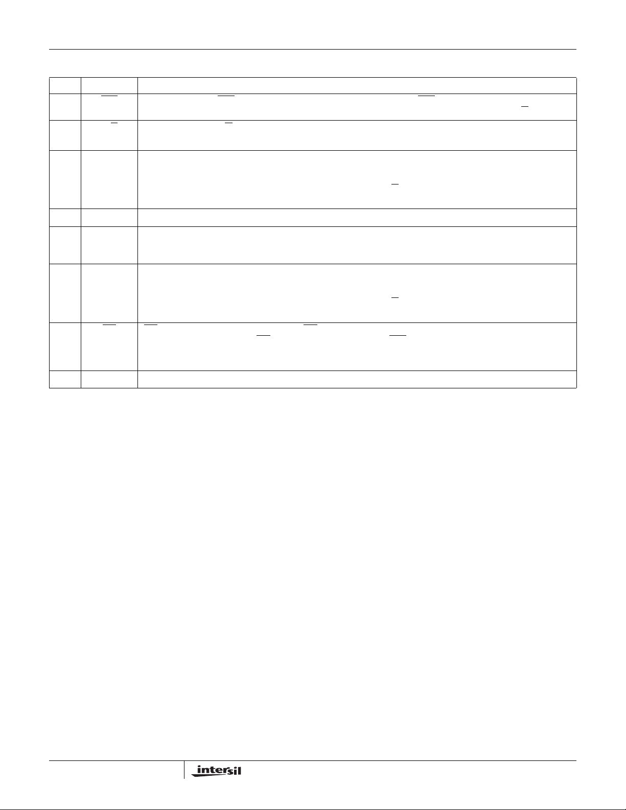
PIN DESCRIPTIONS
Pin Symbol Brief Description
1INCIncrement . The INC input is negative-edge triggered. Toggling INC will move the wiper and either
increment or decrement the counter in the direction indicated by the logic level on the U/D
2U/D
Up/Down. The U/D input controls the direction of the wiper movement and whether the counter
is incremented or decremented.
3R
H/VH
RH/VH. The high (V
) terminals of the X9C102/103/104/503 are equivalent to the fixed
H/RH
terminals of a mechanical potentiometer. The minimum voltage is -5V and the maximum is +5V.
The terminology of V
relation to wiper movement direction selected by the U/D
and VL/RL references the relative position of the terminal in
H/RH
input and not the voltage potential on
the terminal.
4 V
5 V
SS
W/RW
V
SS
VW/R
W. VW/RW
is the wiper terminal, and is equivalent to the movable terminal of a mechanical
potentiometer. The position of the wiper within the array is determined by the control inputs. The
wiper terminal series resistance is typically 40Ω.
6 R
/V
L
RL/V
L
. The low (V
L
terminals of a mechanical potentiometer. The minimum voltage is -5V and the maximum is +5V.
The terminology of V
relation to wiper movement direction selected by the U/D
) terminals of the X9C102/103/104/503 are equivalent to the fixed
L/RL
and VL/RL references the relative position of the terminal in
H/RH
input and not the voltage potential on
the terminal.
7CSCS. The device is selected when the CS input is LOW. The current counter value is stored in
is returned HIGH while the INC input is also HIGH. After the store op-
8 V
CC
nonvolatile memory when CS
eration is complete the X9C102/103/104/503 device will be placed in the low power standby mode
until the device is selected once again.
V
CC
input.
3
FN8222.1
December 20, 2006

X9C102, X9C103, X9C104, X9C503
www.BDTIC.com/Intersil
ABSOLUTE MAXIMUM RATINGS
Temperature under bias .................... -65°C to +135°C
Storage temperature ......................... -65°C to +150°C
Voltage on CS
, INC, U/D and V
CC
with respect to VSS.................................. -1V to +7V
Voltage on V
H/RH
and VL/R
L
referenced to VSS................................... -8V to +8V
ΔV = |V
H/RH
- VL/RL|
X9C102 ............................................................... 4V
X9C103, X9C503, and X9C104 ......................... 10V
Lead temperature (soldering, 10 seconds)...... +300°C
(10 seconds)................................................. 8.8mA
I
W
Power rating X9C102 ........................................ 16mW
Power rating X9C103/104/503 ..........................10mW
RECOMMENDED OPERATING CONDITIONS
Temperature Min. Max.
Commercial 0°C +70°C
Industrial -40°C +85°C
COMMENT
Stresses above those listed under “Absolute Maximum
Ratings” may cause permanent damage to the device.
This is a stress rating only; functional operation of the
device (at these or any other conditions above those
listed in the operational sections of this specification) is
not implied. Exposure to absolute maximum rating
conditions for extended periods may affect device reliability.
Supply Voltage (VCC)
Limits
X9C102/103/104/503 5V ±10%
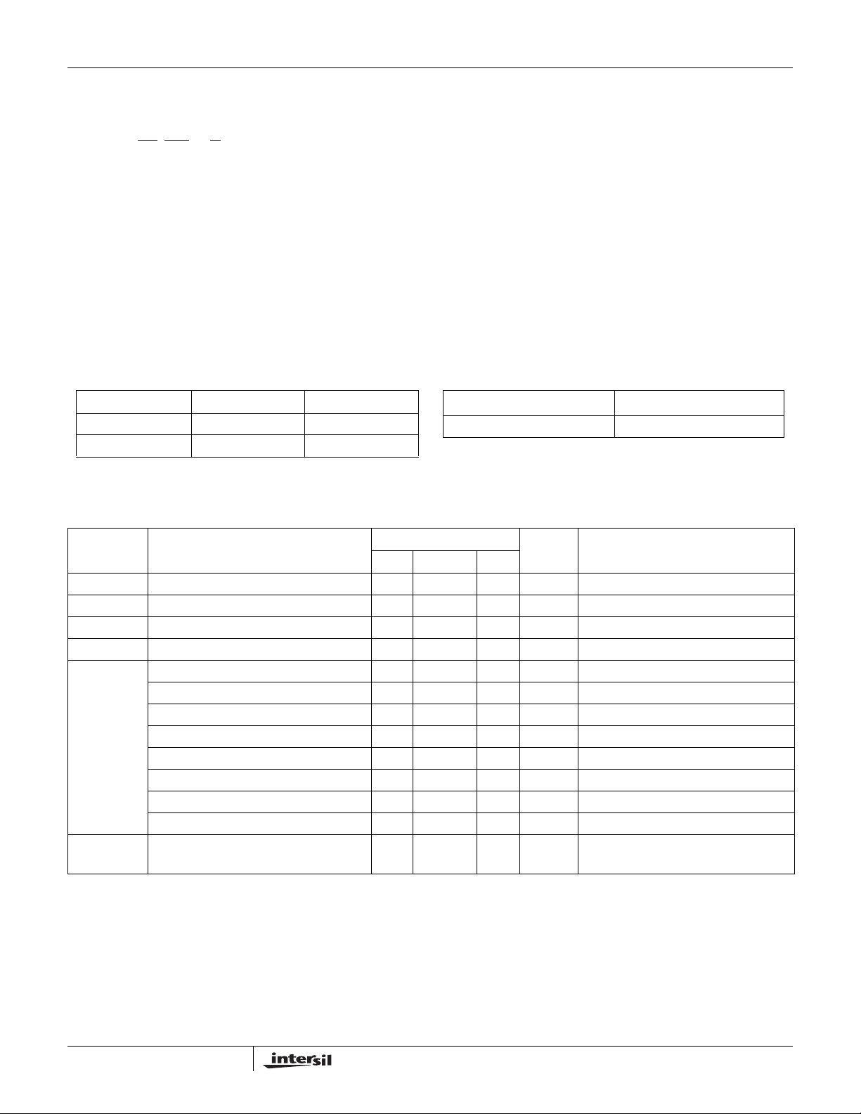
POTENTIOMETER CHARACTERISTICS (Over recommended operating conditions unless otherwise stated.)
Limits
Symbol Parameter
R
TOTAL
V
VH/RH
V
VL/RL
R
I
W
W
End to end resistance variation -20 +20 %
VH terminal voltage -5 +5 V
VL terminal voltage -5 +5 V
Wiper current -4.4 4.4 mA
Wiper resistance 40 100 Ω Wiper Current = ±1mA
(5)
Noise
-120 dBV Ref. 1kHz
Unit Test Conditions/NotesMin. Typ. Max.
Resolution 1 %
(2)
(1)
-1 +1 MI
-0.2 +0.2 MI
Absolute linearity
Relative linearity
RTOTAL temperature coefficient ±300
RTOTAL temperature coefficient ±600
(5)
(5)
(3)
(3)
V
W(n)(actual)
V
W(n + 1)(actual)
- V
W(n)(expected)
ppm/°C X9C103/503/104
ppm/°C X9C102
- [V
W(n) + MI
Ratiometric temperature coefficient ±20 ppm/°C
C
H/CL/CW
(5)
Notes: (1) Absolute linearity is utilized to determine actual wiper voltage versus expected voltage = [V
(2) Relative linearity is a measure of the error in step size between taps = V
(3) 1 MI = Minimum Increment = R
(4) Typical values are for T
(5) This parameter is not 100% tested.
Potentiometer capacitances 10/10/25 pF See Circuit #3, Macro Model
/99
TOT
= +25°C and nominal supply voltage.
A
W(n + 1)
- [V
W(n)(actual)
W(n) + MI
- V
W(n)(expected )
] = +0.2 MI.
] = ±1 MI Maximum.
]
4
FN8222.1
December 20, 2006
 Loading...