

®
X98024
Data Sheet June 6, 2005
240MHz Triple Video Digitizer with
Digital PLL
The X98024 3-channel, 8-bit Analog Front End (AFE)
contains all the components necessary to digitize analog
RGB or YUV graphics signals from personal computers,
workstations and video set-top boxes. The fully differential
analog design provides high PSRR and dynamic
performance to meet the stringent requirements of the
graphics display industry. The AFE’s 240MSPS conversion
rate supports resolutions up to WUXGA at 75Hz refresh rate,
while the front end's high input bandwidth ensures sharp
images at the highest resolutions.
To minimize noise, the X98024's analog section features 2
sets of pseudo-differential RGB inputs with programmable
input bandwidth, as well as internal DC restore clamping
(including mid-scale clamping for YUV signals). This is
followed by the programmable gain/offset stage and the
three 240MSPS Analog-to-Digital Converters (ADCs).
Automatic Black Level Compensation (ABLC™) eliminates
part-to-part offset variation, ensuring perfect black level
performance in every application.
The X98024's digital PLL generates a pixel clock from the
analog source's HSYNC or SOG (Sync-On-Green) signals.
Pixel clock output frequencies range from 10MHz to 240MHz
with sampling clock jitter of 250ps peak to peak.
FN8220.0
Features
• 240MSPS maximum conversion rate
• Low PLL clock jitter (250ps p-p @ 240MSPS)
• 64 interpixel sampling positions
• 0.35V
p-p
to 1.4V
video input range
p-p
• Programmable bandwidth (100MHz to 780MHz)
• 2 channel input multiplexer
• RGB and YUV 4:2:2 output formats
• 5 embedded voltage regulators allow operation from
single 3.3V supply and enhance performance, isolation
• Completely independent 8 bit gain/10 bit offset control
• CSYNC and SOG support
• Trilevel sync detection
• 1.15W typical P
@ 240MSPS
D
• Pb-free plus anneal available (RoHS compliant)
Applications
• LCD Monitors and Projectors
• Digital TVs
• Plasma Display Panels
• RGB Graphics Processing
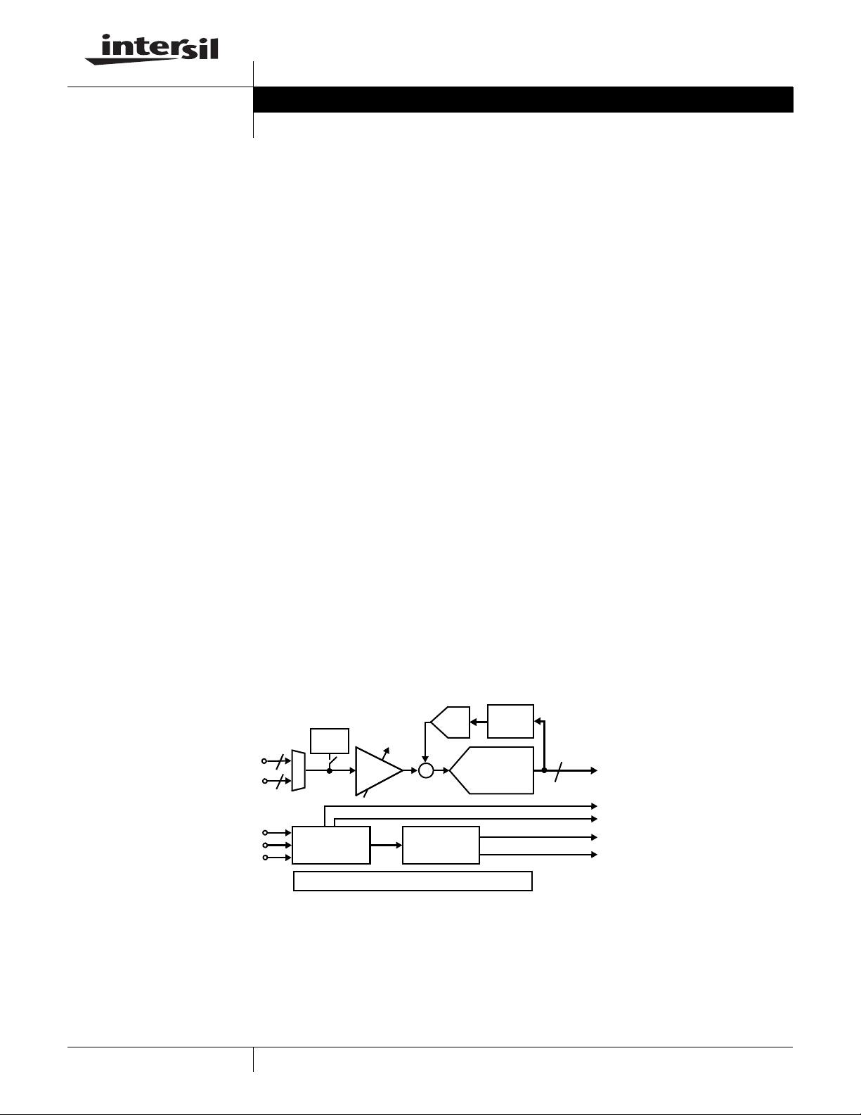
Simplified Block Diagram
RGB/YPbPr
RGB/YPbPr
HSYNC
VSYNC
SOG
1
IN
2
IN
1/2
IN
1/2
IN
1/2
IN
3
3
Voltage
Clamp
PGA
Sync
Processing
AFE Configuration and Control
• Scan Converters
Offset
DAC
+
Digital PLL
8 bit ADC
ABLC™
8 or 16
x3
RGB/YUV
HSYNC
OUT
VSYNC
OUT
HS
OUT
PIXELCLK
OUT
OUT
1
CAUTION: These devices are sensitive to electrostatic discharge; follow proper IC Handling Procedures.
1-888-INTERSIL or 1-888-352-6832
| Intersil (and design) is a registered trademark of Intersil Americas Inc.
All other trademarks mentioned are the property of their respective owners.
Copyright Intersil Americas Inc. 2005. All Rights Reserved
Ordering Information
X98024
PART NUMBER
MAXIMUM PIXEL
RATE
TEMP RANGE
(°C) PACKAGE PART MARKING
X98024L128-3.3 240MHz 0 to 70 128 MQFP X98024L-3.3
X98024L128-3.3-Z
240MHz 0 to 70 128 MQFP (Pb-free) X98024L-3.3Z
(See Note)
NOTE: Intersil Pb-free plus anneal products employ special Pb-free material sets; molding compounds/die attach materials and 100% matte tin plate
termination finish, which are RoHS compliant and compatible with both SnPb and Pb-free soldering operations. Intersil Pb-free products are MSL
classified at Pb-free peak reflow temperatures that meet or exceed the Pb-free requirements of IPC/JEDEC J STD-020.
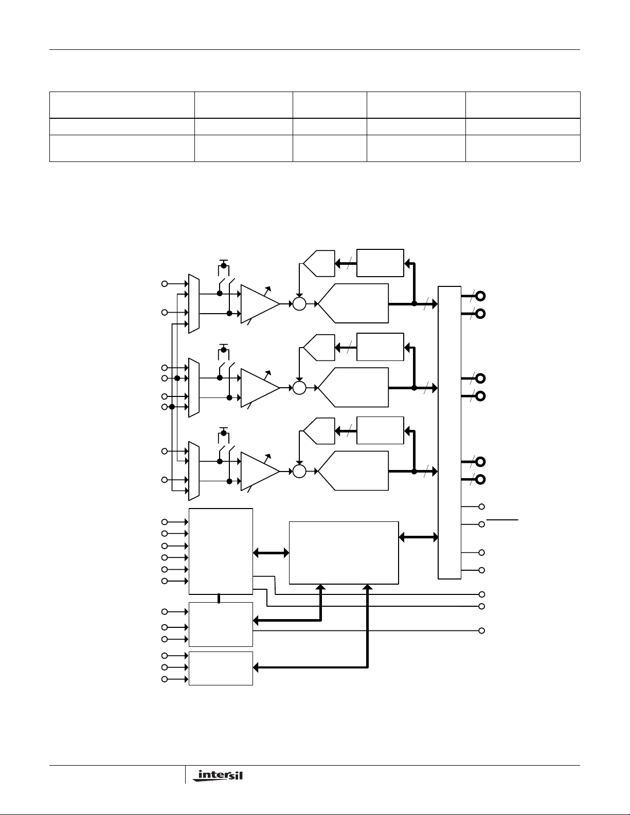
Block Diagram
V
RIN1
RIN2
GIN1
RGB
GND
GIN2
RGB
GND
BIN1
BIN2
SOGIN1
SOG
IN
HSYNCIN1
HSYNC
IN
VSYNCIN1
VSYNC
IN
CLOCKINV
XTAL
XTAL
OUT
SCL
SDA
SADDR
CLAMP
VIN+
-
V
IN
V
1
2
2
VIN+
V
IN
VIN+
V
IN
-
V
-
PGA
CLAMP
PGA
CLAMP
PGA
Sync
2
2
IN
Processing
Digital PLL
Serial
Interface
Offset
+
Offset
+
Offset
+
10
DAC
8 bit ADC
10
DAC
8 bit ADC
10
DAC
8 bit ADC
ABLC™
ABLC™
ABLC™
AFE Configuration
and Control
8
[7:0]
R
8
8
8
P
8
[7:0]
R
S
8
[7:0]
G
P
8
[7:0]
G
S
8
[7:0]
B
P
8
[7:0]
B
S
Output Data Formatter
DATACLK
DATACLK
HS
OUT
VS
OUT
HSYNC
OUT
VSYNC
OUT
XTALCLK
OUT
2
FN8220.0
June 6, 2005
X98024
Absolute Maximum Ratings Recommended Operating Conditions
Voltage on VA, VD, or V
(referenced to GNDA=GNDD=GNDX) . . . . . . . . . . . . . . . . . . . 4.0V
Voltage on any analog input
(referenced to GND
Voltage on any digital input
(referenced to GND
X
pin
) . . . . . . . . . . . . . . . . . . . . . . . . . .-0.3V to VA
A
pin
) . . . . . . . . . . . . . . . . . . . . . . . -0.3V to +6.0V
D
Current into any output pin . . . . . . . . . . . . . . . . . . . . . . . . . . . . . .±20mA
Operating Temperature range . . . . . . . . . . . . . . . . . . . . . 0°C to +70°C
Junction Temperature . . . . . . . . . . . . . . . . . . . . . . . . . . . . . . +125°C
Storage Temperature. . . . . . . . . . . . . . . . . . . . . . . .-65°C to +150°C
CAUTION: Stresses above those listed under “Absolute Maximum Ratings” may cause permanent damage to the device. This is a stress rating only; functional
operation of the device (at these or any other conditions above those listed in the operational sections of this specification) is not implied. Exposure to absolute
maximum rating conditions for extended periods may affect device reliability.
T
Electrical Specifications Specifications apply for V
= VD = VX = 3.3V, pixel rate = 240MHz, f
A
unless otherwise noted
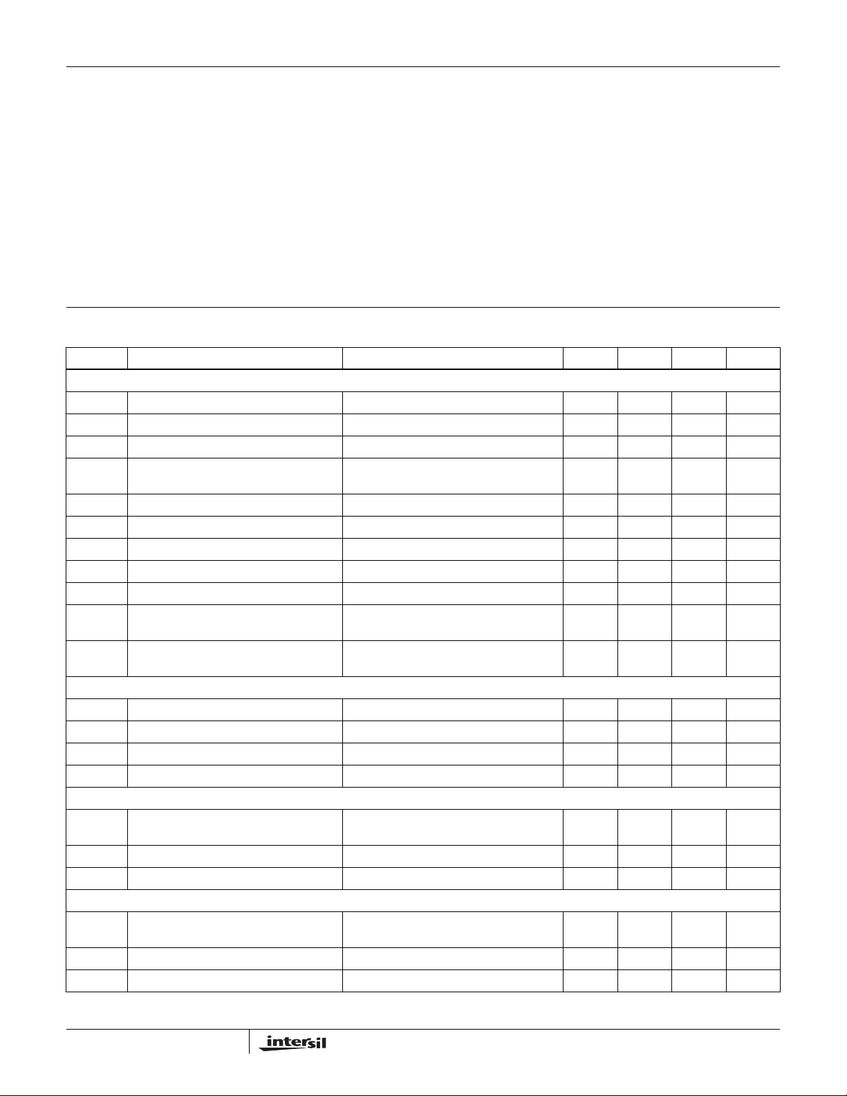
SYMBOL PARAMETER COMMENT MIN TYP MAX UNIT
FULL CHANNEL CHARACTERISTICS
ADC Resolution 8Bits
Missing Codes Guaranteed monotonic None
Conversion Rate Per Channel 10 240 MHz
DNL Differential Non-Linearity 0.6 +1.1
INL Integral Non-Linearity ±1.5 ±3.5 LSB
Gain Adjustment Range ±6 dB
Gain Adjustment Resolution 8Bits
Gain Matching Between Channels Percent of full scale ±1 %
Full Channel Offset Error, ABLC™ enabled ADC LSBs, over time and temperature ±0.125 ±0.5 LSB
Offset Adjustment Range, ABLC™
enabled or disabled
ADC LSBs (see ABLC™ applications
information section)
Overvoltage Recovery Time For 150% overrange, maximum bandwidth
setting
ANALOG VIDEO INPUT CHARACTERISTICS (R
1, GIN1, BIN1, RIN2, GIN2, BIN2)
IN
Input Range 0.35 0.7 1.4 V
Input Bias Current DC restore clamp off ±0.01 ±1 µA
Input Capacitance 5pF
Full Power Bandwidth Programmable 780 MHz
INPUT CHARACTERISTICS (SOG
V
IH/VIL
Input Threshold Voltage Programmable - See Register Listing for
1, SOGIN2)
IN
Details
Hysteresis Centered around threshold voltage 40 mV
Input capacitance 5pF
INPUT CHARACTERISTICS (HSYNC
V
IH/VIL
Input Threshold Voltage Programmable - See Register Listing for
1, HSYNCIN2)
IN
Details
Hysteresis Centered around threshold voltage 240 mV
R
Input impedance 1.2 kΩ
IN
Temperature (Commercial) . . . . . . . . . . . . . . . . . . . . . 0°C to +70°C
Supply Voltage. . . . . . . . . . . . . . . . . . . . . . . . . V
= 25MHz, TA = 25°C,
XTAL
= VD = VX = 3.3V
A
LSB
-0.9
±127 LSB
5ns
P-P
0 to
V
-0.3
0.4 to 3.2 V
3
FN8220.0
June 6, 2005
X98024
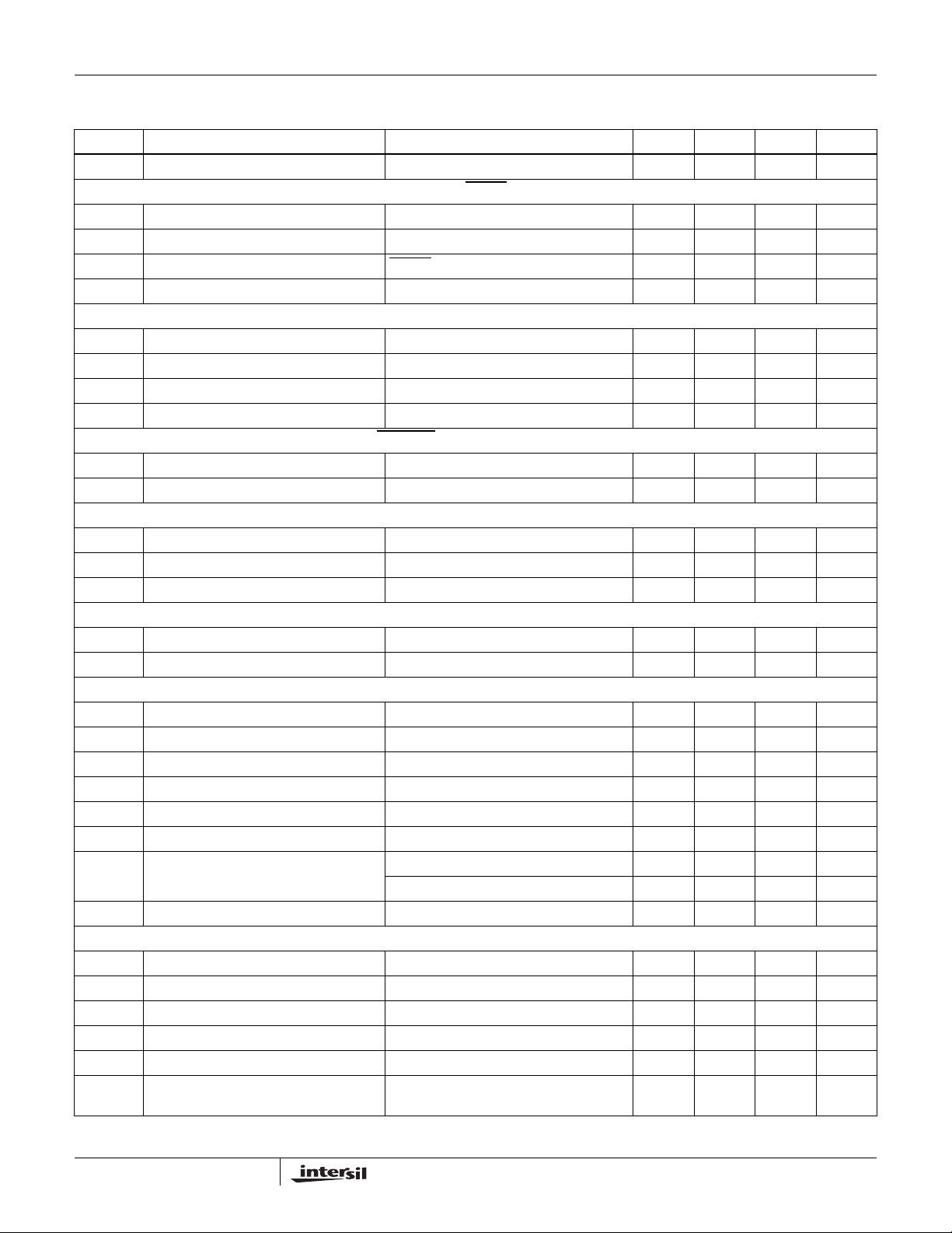
Electrical Specifications Specifications apply for V
= VD = VX = 3.3V, pixel rate = 240MHz, f
A
= 25MHz, TA = 25°C,
XTAL
unless otherwise noted (Continued)
SYMBOL PARAMETER COMMENT MIN TYP MAX UNIT
Input capacitance 5pF
DIGITAL INPUT CHARACTERISTICS (SDA, SADDR, CLOCKINV
V
V
Input HIGH Voltage 2.0 V
IH
Input LOW Voltage 0.8 V
IL
I Input leakage current RESET
, RESET)
IN
has a 70kΩ pullup to V
D
±10 nA
Input capacitance 5pF
SCHMITT DIGITAL INPUT CHARACTERISTICS (SCL, VSYNC
V
+ Low to High Threshold Voltage 1.45 V
T
1, VSYNCIN2)
IN
VT- High to Low Threshold Voltage 0.95 V
I Input leakage current ±10 nA
Input capacitance 5pF
DIGITAL OUTPUT CHARACTERISTICS (DATACLK, DATACLK
V
V
DIGITAL OUTPUT CHARACTERISTICS (R
V
V
R
Output HIGH Voltage, IO = 16mA 2.4 V
OH
Output LOW Voltage, IO = -16mA 0.4 V
OL
, GP, BP, RS, GS, BS, HS
P
Output HIGH Voltage, IO = 8mA 2.4 V
OH
Output LOW Voltage, IO = -8mA 0.4 V
OL
Pulldown to GNDD when three-state RP, GP, BP, RS, GS, BS only 58 kΩ
TRI
DIGITAL OUTPUT CHARACTERISTICS (SDA, XTALCLK
V
V
Output HIGH Voltage, IO = 4mA XTALCLK
OH
Output LOW Voltage, IO = -4mA 0.4 V
OL
OUT
)
, VS
OUT
OUT
, HSYNC
OUT
, VSYNC
OUT
)
)
only; SDA is open-drain 2.4 V
OUT
POWER SUPPLY REQUIREMENTS
V
V
V
P
Analog Supply Voltage 3 3.3 3.6 V
A
Digital Supply Voltage 3 3.3 3.6 V
D
Crystal Oscillator Supply Voltage 3 3.3 3.6 V
X
I
Analog Supply Current Operating 190 200 mA
A
I
Digital Supply Current Operating (grayscale) 160 170 mA
D
I
Crystal Oscillator Supply Current 0.7 2 mA
X
Total Power Dissipation Operating (average) 1.15 1.35 W
D
Power-down Mode 50 80 mW
Θ
Thermal Resistance, Junction to Ambient 30 °C/W
JA
AC TIMING CHARACTERISTICS
PLL Jitter 250 450 ps p-p
Sampling Phase Steps 5.6° per step 64
Sampling Phase Tempco ±1 ps/°C
Sampling Phase Differential Nonlinearity Degrees out of 360° ±3 °
HSYNC Frequency Range 10 150 kHz
f
XTAL
Crystal Frequency Range 23
25 27 MHz
(Note 2)
4
FN8220.0
June 6, 2005
X98024
Electrical Specifications Specifications apply for V
= VD = VX = 3.3V, pixel rate = 240MHz, f
A
= 25MHz, TA = 25°C,
XTAL
unless otherwise noted (Continued)
SYMBOL PARAMETER COMMENT MIN TYP MAX UNIT
t
SETUP
DATA valid before rising edge of DATACLK 15pF DATACLK load, 15pF DATA load
1.3 ns
(Note 1)
t
HOLD
DATA valid after rising edge of DATACLK 15pF DATACLK load, 15pF DATA load
(Note 1)
2.0 ns
AC TIMING CHARACTERISTICS (2 WIRE INTERFACE)
f
SCL
SCL Clock Frequency 0 400 kHz
Maximum width of a glitch on SCL that will
2 XTAL periods min 80 ns
be suppressed
t
t
BUF
t
LOW
t
HIGH
t
SU:STA
t
HD:STA
t
SU:DAT
t
HD:DAT
t
SU:STO
t
SCL LOW to SDA Data Out Valid 5 XTAL periods plus SDA’s RC time
AA
constant
Time the bus must be free before a new
1.3 µs
See
comment
transmission can start
Clock LOW Time 1.3 µs
Clock HIGH Time 0.6 µs
Start Condition Setup Time 0.6 µs
Start Condition Hold Time 0.6 µs
Data In Setup Time 100 ns
Data In Hold Time 0ns
Stop Condition Setup Time 0.6 µs
Data Output Hold Time 4 XTAL periods min 160 ns
DH
NOTES:
1. Setup and hold times are at a 140MHz DATACLK rate.
2. For X98024, register 0x2B must be set to 0x15 for crystal frequencies below 24.5MHz
µs
SCL
SDA IN
SDA OUT
DATACLK
DATACLK
Pixel Data
t
SU:ST
t
HD:STA
t
F
t
SU:DAT
t
HIGH
t
LOW
t
HD:DAT
t
R
FIGURE 1. 2 WIRE INTERFACE TIMING
t
t
SETUP
HOLD
FIGURE 2. DATA OUTPUT SETUP AND HOLD TIMING
t
SU:STO
t
t
DH
AA
t
BUF
5
FN8220.0
June 6, 2005
X98024
HSYNC
Analog
Video In
DATACLK
RP/GP/BP[7:0]
RS/GS/BS[7:0]
HS
OUT
HSYNC
Analog
Video In
IN
P
P
0
1
The HSYNC edge (programmable leading or trailing) that the DPLL is locked to.
The sampling phase setting determines its relative position to the rest of the AFE’s output signals
t
HSYNCin-to-HSout
P
2
= 7.5ns + (PHASE/64 +8.5)*t
P
P
3
P
4
5
P
PIXEL
6
P
P
7
P
8
P
9
10
P
P
11
12
8.5 DATACLK Pipeline Latency
D
D
0
D
1
D
2
3
Programmable
Width and Polarity
FIGURE 3. 24 BIT OUTPUT MODE
IN
The HSYNC edge (programmable leading or trailing) that the DPLL is locked to.
The sampling phas e setting dete rmines its relativ e position to th e rest of the A F E’s output sig nals
t
HSYNCin-to-HSout
P
P
0
P
1
= 7.5ns + (PHASE/64 +8.5)*t
P
2
3
PIXEL
P
P
4
P
5
P
6
P
7
8
P
P
9
P
10
P
11
12
DATACLK
GP[7:0]
RP[7:0]
BP[7:0]
HS
OUT
8.5 DATACLK Pipeline Latency
Programmable
Width and Polarity
FIGURE 4. 24 BIT 4:2:2 OUTPUT MODE (FOR YUV SIGNALS)
G0 (Yo) G1 (Y1)G2 (Y2)
(Uo)R1 (V1)B2 (U2)
B
0
6
FN8220.0
June 6, 2005
X98024
HSYNC
Analog
Video In
DATACLK
RP/GP/BP[7:0]
RS/GS/BS[7:0]
HS
OUT
HSYNC
IN
P
0
The HSY NC edge (programm able leading or trailing) that the DPLL is locked to.
The s a mpling p h a s e se ttin g d e te rmine s its r ela tiv e po s itio n to th e r e st o f th e AFE’s o u tp ut sig n a ls
t
HSYNCin-to-HSout
P
P
1
2
= 7.5ns + (PHASE/64 +10.5)*t
P
P
3
4
PIXEL
P
P
P
P
5
6
7
P
8
9
P
P
10
P
11
12
D
0
D
1
D
2
D
3
Programmable
Width and Polarity
FIGURE 5. 48 BIT OUTPUT MODE
The HSYNC edge (programm a b le lea d ing or trailing) that th e D PLL is lo c k e d t o.
IN
The HSYNC edge (programmable leading or trailing) that th e D PL L is locked t o .
The sampling phase setting determines its relative position to the rest of the AFE’s output signals
t
HSYNCin-to-HSout
= 7.5ns + (PHASE/64 +8.5)*t
PIXEL
Analog
Video In
P
0
P
P
P
P
P
P
P
P
P
1
2
3
4
5
6
7
8
P
9
10
DATACLK
RP/GP/BP[7:0] D
RS/GS/BS[7:0]
HS
OUT
Programmable
Width and Polarity
D
0
D
1
FIGURE 6. 48 BIT OUTPUT MODE, INTERLEAVED TIMING
P
11
2
7
FN8220.0
June 6, 2005
Pinout
NC
NC
GND
V
BYPASS
GND
RIN1
GND
V
BYPASS
GND
GIN1
RGB
GND
SOG
IN
GND
V
BYPASS
GND
BIN1
GND
RIN2
GND
GIN2
RGB
GND
SOG
IN
GND
BIN2
GND
V
COREADC
GND
HSY NCIN1
HSY NC
IN
GND
GND
X98024
X98024
(128-PIN MQFP)
TOP VIEW
OUT
OUT
OUT
OUT
HSY NC
VS
HS
126
125
VDGNDDDATAC L K
124
123
122
VSYNC
128
127
1
2
3
A
4
5
A
6
V
A
7
8
A
9
10
A
11
V
A
12
13
1
14
1
15
A
16
17
A
18
V
A
19
20
V
A
21
A
22
23
A
24
25
2
26
2
27
A
28
29
V
A
30
A
31
32
D
33
34
2
35
V
A
36
A
37
X
38
V
X
DATAC L K
121
GNDDR
120
0
P
119
1
P
R
118
2
P
R
117
3
P
R
116
4
P
R
115
5
P
R
114
6
P
R
113
7
P
R
112
D
V
111
GNDDV
110
CORE
109
GNDDR
108
0
S
107
1
S
R
106
2
S
R
105
3
S
R
104
4
S
R
103
102
101
100
99
98
97
96
95
94
93
92
91
90
89
88
87
86
85
84
83
82
81
80
79
78
77
76
75
74
73
72
71
70
69
68
67
66
65
RS5
R
6
S
R
7
S
V
D
GND
GP0
G
1
P
G
2
P
G
3
P
G
4
P
G
5
P
G
6
P
G
7
P
V
D
GND
GS0
G
1
S
G
2
S
G
3
S
G
4
S
5
G
S
G
6
S
G
7
S
V
CORE
GND
V
D
GND
BP0
B
1
P
2
B
P
3
B
P
B
4
P
5
B
P
6
B
P
7
B
P
V
D
GND
VRE G
D
D
D
D
D
IN
39404142434445464748495051525354555657585960616263
1
2
IN
OUT
XTAL
XTAL
D
IN
CLOCKINV
IN
PLL
V
IN
GND
VSYNC
OUT
RESET
S ADDR
VSYNC
D
SCL
SDA
CORE
GND
V
DVD
GND
7
6
5
4
3
2
1
S
S
S
S
B
B
S
B
B
B
0
S
S
S
B
B
B
XTALCLOCK
8
NC
64
OUT
VRE G
FN8220.0
June 6, 2005
X98024
Pin Descriptions
SYMBOL PIN DESCRIPTION
R
1 7 Analog input. Red channel 1. DC couple or AC couple through 0.1µF.
IN
G
1 12 Analog input. Green channel 1. DC couple or AC couple through 0.1µF.
IN
1 19 Analog input. Blue channel 1. DC couple or AC couple through 0.1µF.
B
IN
RGB
HSYNC
VSYNC
RGB
HSYNC
VSYNC
CLOCKINV
XTAL
XTALCLK
DATACLK 121 3.3V digital output. Data clock output. Equal to pixel clock rate in 24 bit mode, one half pixel clock rate in 48
DATACLK
1 13 Analog input. Ground reference for the R, G, and B inputs of channel 1 in the DC coupled configuration.
GND
Connect to the same ground as channel 1's R, G, and B termination resistors. This signal is not used in the
AC-coupled configuration, but the pin should still be tied to GND
SOG
1 14 Analog input. Sync on Green. Connect to GIN1 through a 0.01µF capacitor in series with a 500Ω resistor.
IN
1 33 Digital input, 5V tolerant, 240mV hysteresis, 1.2kΩ impedance to GNDA. Connect to channel 1's HSYNC
IN
1 44 Digital input, 5V tolerant, 500mV hysteresis. Connect to channel 1's VSYNC signal.
IN
R
2 22 Analog input. Red channel 2. DC couple or AC couple through 0.1µF.
IN
signal through a 680Ω series resistor.
.
A
GIN2 24 Analog input. Green channel 2. DC couple or AC couple through 0.1µF.
B
2 28 Analog input. Blue channel 2. DC couple or AC couple through 0.1µF.
IN
2 25 Analog input. Ground reference for the R, G, and B inputs of channel 2 in the DC coupled configuration.
GND
SOG
2 26 Analog input. Sync on Green. Connect to GIN1 through a 0.01µF capacitor in series with a 500Ω resistor.
IN
2 34 Digital input, 5V tolerant, 240mV hysteresis, 1.2kΩ impedance to GNDA. Connect to channel 2's HSYNC
IN
2 45 Digital input, 5V tolerant, 500mV hysteresis. Connect to channel 2's VSYNC signal.
IN
41 Digital input, 5V tolerant. When high, changes the pixel sampling phase by 180 degrees. Toggle at frame
46 Digital input, 5V tolerant, active low, 70kΩ pull-up to VD. Take low for at least 1µs and then high again to
39 Analog input. Connect to external 23MHz to 27MHz crystal and load capacitor (see crystal spec for
40 Analog output. Connect to external 23MHz to 27MHz crystal and load capacitor (see crystal spec for
47 3.3V digital output. Buffered crystal clock output at f
RESET
XTAL
OUT
IN
IN
OUT
Connect to the same ground as channel 1's R, G, and B termination resistors. This signal is not used in the
AC-coupled configuration, but the pin should still be tied to GND
.
A
signal through a 680Ω series resistor.
rate during VSYNC to allow 2x undersampling to sample odd and even pixels on sequential frames. Tie to
D
if unused.
GND
reset the X98024. This pin is not necessary for normal use and may be tied directly to the V
recommended loading). Typical oscillation amplitude is 1.0V
recommended loading). Typical oscillation amplitude is 1.0V
system components.
XTAL
centered around 0.5V.
P-P
centered around 0.5V.
P-P
or f
/2. May be used as system clock for other
XTAL
supply.
D
SADDR 48 Digital input, 5V tolerant. Address = 0x4C (0x98 including R/W bit) when tied low. Address = 0x4D (0x9A
including R/W bit) when tied high.
SCL 50 Digital input, 5V tolerant, 500mV hysteresis. Serial data clock for 2-wire interface.
SDA 49 Bidirectional Digital I/O, open drain, 5V tolerant. Serial data I/O for 2-wire interface.
R
[7:0] 112-119 3.3V digital output. Red channel, primary pixel data. 58K pulldown when three-stated.
P
[7:0] 100-107 3.3V digital output. Red channel, secondary pixel data. 58K pulldown when three-stated.
R
S
G
[7:0] 90-97 3.3V digital output. Green channel, primary pixel data. 58K pulldown when three-stated.
P
G
[7:0] 80-87 3.3V digital output. Green channel, secondary pixel data. 58K pulldown when three-stated.
S
[7:0] 68-75 3.3V digital output. Blue channel, primary pixel data. 58K pulldown when three-stated.
B
P
B
[7:0] 55-62 3.3V digital output. Blue channel, secondary pixel data. 58K pulldown when three-stated.
S
bit mode.
122 3.3V digital output. Inverse of DATACLK.
9
FN8220.0
June 6, 2005

X98024
Pin Descriptions (Continued)
SYMBOL PIN DESCRIPTION
HS
OUT
VS
OUT
HSYNC
OUT
VSYNC
OUT
V
A
GND
A
V
D
GND
D
V
X
GND
X
V
BYPASS
VREG
IN
VREG
OUT
V
COREADC
V
PLL
V
CORE
NC 1, 2, 63 Reserved. Do not connect anything to these pins.
125 3.3V digital output. HSYNC output aligned with pixel data. Use this output to frame the digital output data.
This output is always purely horizontal sync (without any composite sync signals)
126 3.3V digital output.Artificial VSYNC output aligned with pixel data. VSYNC is generated 8 pixel clocks after
the trailing edge of HS
. This signal is usually not needed - use VSYNC
OUT
127 3.3V digital output. Buffered HSYNC (or SOG or CSYNC) output. This is typically used to measure HSYNC
period. HS
and Macrovision signals if present on HSYNC
should be used to detect the beginning of a line. This output will pass composite sync signals
OUT
or SOGIN.
IN
128 3.3V digital output. Buffered VSYNC output. For composite sync signals, this output will be asserted for the
duration of the disruption of the normal HSYNC pattern. This is typically used to detect the beginning of a
frame and measure the VSYNC period.
6, 11, 18, 20,
Power supply for the analog section. Connect to a 3.3V supply and bypass each pin to GNDA with 0.1µF.
29, 35
3, 5, 8, 10, 15,
17, 21, 23, 27,
Ground return for V
and V
A
BYPASS
.
30, 36
54, 67, 77, 89,
Power supply for all digital I/Os. Connect to a 3.3V supply and bypass each pin to GNDD with 0.1µF.
99, 111, 124
32, 43, 51, 53,
Ground return for V
, V
D
CORE
, V
COREADC
, and V
66, 76, 78, 88,
98, 108, 110,
120, 123
38 Power supply for crystal oscillator. Connect to a 3.3V supply and bypass to GNDX with 0.1µF.
37 Ground return for VX.
4, 9, 16 Bypass these pins to GNDA with 0.1µF. Do not connect these pins to each other or anything else.
65 3.3V input voltage for V
64 Regulated output voltage for V
V
COREADC
output can only supply power to V
and V
CORE
voltage regulator. Connect to a 3.3V source, and bypass to GNDD with 0.1µF.
CORE
, V
PLL
and bypass at input pins as instructed below. Do not connect to anything else - this
COREADC
, V
PLL
and V
COREADC
31 Internal power for the ADC’s digital logic. Connect to VREG
with 0.1µF.
42 Internal power for the PLL’s digital logic. Connect to VREG
with 0.1µF.
52, 79, 109 Internal power for core logic. Connect to VREG
OUT
as VSYNC source.
OUT
.
PLL
; typically 1.9V. Connect only to V
CORE
and V
.
CORE
through a 10Ω resistor and bypass to GNDD
OUT
through a 10Ω resistor and bypass to GNDD
OUT
and bypass each pin to GNDD with 0.1µF.
PLL
,
10
FN8220.0
June 6, 2005

X98024
Register Listing
ADDRESS REGISTER (DEFAULT VALUE) BIT(s) FUNCTION NAME DESCRIPTION
0x01 SYNC Status
(read only)
0x02 SYNC Polarity
(read only)
0x03 HSYNC Slicer (0x44) 2:0 HSYNC1 Threshold 000 = lowest (0.4V) All values referred to
0x04 SOG Slicer (0x08) 3:0 SOG1 and SOG2
0 HSYNC1 Active 0: HSYNC1 is Inactive
1: HSYNC1 is Active
1 HSYNC2 Active 0: HSYNC2 is Inactive
1: HSYNC2 is Active
2 VSYNC1 Active 0: VSYNC1 is Inactive
3 VSYNC2 Active 0: VSYNC2 is Inactive
4 SOG1 Active 0: SOG1 is Inactive
5 SOG2 Active 0: SOG2 is Inactive
6 PLL Locked 0: PLL is unlocked
7 CSYNC Detected at
Sync Splitter Output
0 HSYNC1
Polarity
1 HSYNC2
Polarity
2VSYNC1
Polarity
3VSYNC2
Polarity
4 HSYNC1
Trilevel
5 HSYNC2
Trilevel
7:6 N/A Returns 0
3 Reserved Set to 00
6:4 HSYNC2 Threshold See HSYNC1
7 Disable Glitch Filter 0: HSYNC/VSYNC Digital Glitch Filter Enabled (default)
Threshold
4 SOG Filter
Enable
5SOG Hysteresis
Disable
7:6 Reserved Set to 00.
1: VSYNC1 is Active
1: VSYNC2 is Active
1: SOG1 is Active
1: SOG2 is Active
1: PLL is locked to incoming HSYNC
0: Composite Sync signal not detected
1: Composite Sync signal is detected
0: HSYNC1 is Active High
1: HSYNC1 is Active Low
0: HSYNC2 is Active High
1: HSYNC2 is Active Low
0: VSYNC1 is Active High
1: VSYNC1 is Active Low
0: VSYNC2 is Active High
1: VSYNC2 is Active Low
0: HSYNC1 is Standard Sync
1: HSYNC1 is Trilevel Sync
0: HSYNC2 is Standard Sync
1: HSYNC2 is Trilevel Sync
100 = default (2.0V) voltage at HSYNC input
111 = highest (3.2V) pin, 240mV hysteresis
1: HSYNC/VSYNC Digital Glitch Filter Disabled
0x0 = lowest (0mV) 40mV hysteresis at
0x8 = default (160mV) all settings
0xF = highest (300mV) 20mV step size
0: SOG low pass filter disabled (default)
1: SOG low pass filter enabled, 14MHz corner
0: 40mV SOG hysteresis enabled
1: 40mV SOG hysteresis disabled (default)
11
FN8220.0
June 6, 2005

X98024
Register Listing (Continued)
ADDRESS REGISTER (DEFAULT VALUE) BIT(s) FUNCTION NAME DESCRIPTION
0x05 Input configuration (0x00) 0 Channel Select 0: VGA1
1 Input Coupling 0: AC coupled (positive input connected to clamp DAC
2 RGB/YUV 0: RGB inputs (Clamp DAC = 300mV for R, G, B, half scale
3 Sync Type 0: Separate HSYNC/VSYNC
4 Composite Sync
Source
5 COAST CLAMP
enable
7:6 Reserved Set to 00.
0x06 Red Gain (0x55) 7:0 Red Gain Channel gain, where:
1: VGA2
during clamp time, negative input disconnected from outside
pad and always internally tied to appropriate clamp DAC)
1: DC coupled (+ and - inputs are brought to pads and never
connected to clamp DACs). Analog clamp signal is turned off
in this mode.
analog shift for R, G , and B, base ABLC™ target code = 0x00
for R, G, and B)
1: YUV inputs (Clamp DAC = 600mV for R and B, 300mV for
G, half scale analog shift for G channel only, base ABLC™
target code = 0x00 for G, = 0x80 for R and B)
1: Composite (from SOG or CSYNC on HSYNC)
0: SOG
IN
1: HSYNC
Note: If Sync Type = 0, the multiplexer will pass HSYNCIN
regardless of the state of this bit.
0: DC restore clamping and ABLC™ suspended during
COAST
1: DC restore clamping and ABLC™ continue during COAST
gain (V/V) = 0.5 + [7:0]/170
IN
0x07 Green Gain (0x55) 7:0 Green Gain
0x08 Blue Gain (0x55) 7:0 Blue Gain
0x09 Red Offset (0x80) 7:0 Red Offset ABLC™ enabled: digital offset control. A 1 LSB change in
0x0A Green Offset (0x80) 7:0 Green Offset
0x0B Blue Offset (0x80) 7:0 Blue Offset
0x0C Offset DAC Configuration (0x00) 0 Offset DAC Range 0: ±1/2 ADC fullscale (1 DAC LSB ~ 1 ADC LSB)
1 Reserved Set to 0.
3:2 Red Offset DAC LSBs These bits are the LSBs necessary for 10 bit manual offset
5:4 Green Offset DAC
LSBs
7:6 Blue Offset DAC
LSBs
0x00: gain = 0.5 V/V
(1.4VP-P input = full range of ADC)
0x55: gain = 1.0 V/V
(0.7VP-P input = full range of ADC)
0xFF: gain = 2.0 V/V
(0.35VP-P input = full range of ADC)
this register will shift the ADC output by 1 LSB.
ABLC™ disabled: analog offset control. These bits go to the
upper 8 bits of the 10 bit offset DAC. A 1LSB change in this
register will shift the ADC output approximately 1 LSB (Offset
DAC range = 0) or 0.5LSBs (Offset DAC range = 1).
0x00 = min DAC value or -0x80 digital offset,
0x80 = mid DAC value or 0x00 digital offset,
0xFF = max DAC value or +0x7F digital offset
1: ±1/4 ADC fullscale (1 DAC LSB ~ 1/2 ADC LSB)
DAC control.
Combine with their respective MSBs in registers 0x09, 0x0A,
and 0x0B to achieve 10 bit offset DAC control.
12
FN8220.0
June 6, 2005

X98024
Register Listing (Continued)
ADDRESS REGISTER (DEFAULT VALUE) BIT(s) FUNCTION NAME DESCRIPTION
0x0D AFE Bandwidth (0x0E) 0 Unused Value doesn’t matter
3:1 AFE BW 3dB point for AFE lowpass filter
000: 100MHz
111: 780MHz (default)
7:4 Peaking 0000: Disabled (default) See Bandwidth and Peaking
Control section for more information
0x0E PLL Htotal MSB (0x03) 5:0 PLL Htotal MSB 14 bit HTOTAL (number of active pixels) value
0x0F PLL Htotal LSB (0x20) 7:0 PLL Htotal LSB
0x10 PLL Sampling Phase (0x00) 5:0 PLL Sampling Phase Used to control the phase of the ADC’ s sample point relative
0x11 PLL Pre-coast (0x08) 7:0 Pre-coast Number of lines the PLL will coast prior to the start of
0x12 PLL Post-coast (0x00) 7:0 Post-coast Number of lines the PLL will coast after the end of VSYNC.
0x13 PLL Misc (0x00) 0 PLL Lock Edge
HSYNC1
1 PLL Lock Edge
HSYNC2
2 Reserved Set to 0.
3CLKINV
Disable
5:4 CLKINV
IN
IN
Pin
Pin
Function
6 XTALCLKOUT
Frequency
7 Disable
XTALCLKOUT
0x14 DC Restore and ABLC™ starting
pixel MSB (0x00)
4:0 DC Restore and
ABLC™ starting
pixel (MSB)
0x15 DC Restore and ABLC™ starting
pixel LSB (0x00)
7:0 DC Restore and
ABLC™ starting
pixel (LSB)
0x16 DC Restore Clamp Width
(0x10)
7:0 DC Restore clamp
width (pixels)
The minimum HTOTAL value supported is 0x200.
HTOTAL to PLL is updated on LSB write only.
to the period of a pixel. Adjust to obtain optimum image
quality. One step = 5.625° (1.56% of pixel period).
VSYNC. Applies only to internally generated COAST
signals.
Applies only to internally generated COAST signals.
0: Lock on trailing edge of HSYNC1 (default)
1: Lock on leading edge of HSYNC1
0: Lock on trailing edge of HSYNC2 (default)
1: Lock on leading edge of HSYNC2
0: CLKINVIN pin enabled (default)
1: CLKINV
pin disabled (internally forced low)
IN
00: CLKINV (default)
01: External CLAMP (see Note)
10: External COAST
11: External PIXCLK
Note: the CLAMP pulse is used to
- perform a DC restore (if enabled)
- start the ABLC™ function (if enabled), and
- update the data to the Offset DACs (always).
When in the default internal CLAMP mode, the X98024
automatically generates the CLAMP pulse. If External
CLAMP is selected, the Offset DAC values will only change
on the leading edge of CLAMP. If there is no internal clamp
signal, there will be up to a 100ms delay between when the
PGA gain or offset DAC register is written to, and when the
PGA or offset DAC is actually updated.
0: XTALCLK
1: XTALCLK
0 = XTALCLK
1 = XTALCLK
Pixel after HSYNC
DC restore and ABLC™ functions. 13 bits.
= f
OUT
CRYSTAL
= f
OUT
CRYSTAL
enabled
OUT
is logic low
OUT
trailing edge to begin
IN
(default)
/2
Set this register to the first stable black pixel following the
trailing edge of HSYNC
.
IN
Width of DC restore clamp used in AC-coupled
configurations. Has no effect on ABLC™. Minimum value is
0x02 (a setting of 0x01 or 0x00 will not generate a clamp
pulse).
13
FN8220.0
June 6, 2005

X98024
Register Listing (Continued)
ADDRESS REGISTER (DEFAULT VALUE) BIT(s) FUNCTION NAME DESCRIPTION
0x17 ABLC™ Configuration (0x40) 0 ABLC™ disable 0: ABLC™ enabled (default)
1 Reserved Set to 0.
3:2 ABLC™ pixel width Number of black pixels averaged every line for ABLC™
6:4 ABLC™ bandwidth ABLC™ Time constant (lines) = 2
7 Reserved Set to 0.
0x18 Output Format (0x00) 0 Bus Width 0: 24 bits: Data output on R
1 Interleaving
(48 bit mode only)
2Bus Swap
(48 bit mode only)
3 Reserved Set to 0.
4 422
(24 bit mode only)
5DATACLK
Polarity
6 VSOUT Polarity 0: Active High (default)
7 HSOUT Polarity 0: Active High (default)
0x19 HSOUT Width (0x10) 7:0 HSOUT Width HSOUT width, in pixels. Minimum value is 0x01 for 24 bit
0x1A Output Signal Disable (0x00) 0 Three-state R
1 Three-state R
2 Three-state G
3 Three-state G
4 Three-state B
5 Three-state B
P
S
P
S
P
S
[7:0]
[7:0]
6 Three-state
DATACLK
7 Three-state
DATACLK
1: ABLC™ disabled
function
00: 16 pixels [default]
01: 32 pixels
10: 64 pixels
11: 128 pixels
000 = 32 lines
100 = 256 lines (default)
111 = 4096 lines
driven low (default)
1: 48 bits: Data output on R
0: No interleaving: data changes on same edge of DAT ACLK
(default)
1: Interleaved: Secondary databus data changes on
opposite edge of DATACLK from primary databus
0: First data byte after trailing edge of HSOUT appears on
R
, GP, BP (default)
P
1: First data byte after trailing edge of HSOUT appears on
R
, GS, BS (primary and secondary busses are reversed)
S
0: Data is formatted as 4:4:4 (RGB, default)
1: Data is decimated to 4:2:2 (YUV), blue channel is driven
low
0: HS
DATACLK (default)
1: HS
DATACLK
OUT
OUT
, VS
, and Pixel Data change on falling edge of
OUT
, VS
, and Pixel Data change on rising edge of
OUT
1: Active Low
1: Active Low
modes, 0x02 for 48 bit modes.
[7:0] 0 = Output byte enabled
1 = Output byte three-stated
[7:0]
These bits override all other I/O settings
Output data pins have 58kΩ pulldown resistors to GND
[7:0]
[7:0]
0 = DATACLK enabled
1 = DATACLK
three-stated
0 = DATACLK enabled
1 = DATACLK three-stated
(5+[6:4])
, GP, BP only; RS, GS, BS are all
P
, GP, BP, RS, GS, B
P
S
.
D
14
FN8220.0
June 6, 2005

X98024
Register Listing (Continued)
ADDRESS REGISTER (DEFAULT VALUE) BIT(s) FUNCTION NAME DESCRIPTION
0x1B Power Control (0x00) 0 Red
Power-down
1 Green
Power-down
2Blue
Power-down
3PLL
Power-down
7:4 Reserved Set to 0
0x1C Reserved (0x47) 7:0 Reserved Set to 0x49 for best performance with NTSC and PAL video
0x23 DC Restore Clamp (0x08) 3:0 Reserved Set to 1000
6:4 DC Restore Clamp
Impedance
7 Reserved Set to 0
0 = Red ADC operational (default)
1 = Red ADC powered down
0 = Green ADC operational (default)
1 = Green ADC powered down
0 = Blue ADC operational (default)
1 = Blue ADC powered down
0 = PLL operational (default)
1 = PLL powered down
DC Restore clamp's ON resistance.
Shared for all three channels
0: Infinite (clamp disconnected) (default)
1: 1600Ω
2: 800Ω
3: 533Ω
4: 400Ω
5: 320Ω
6: 267Ω
7: 228Ω
Technical Highlights
The X98024 provides all the features of traditional triple
channel video AFEs, but adds several next-generation
enhancements, bringing performance and ease of use to
new levels.
DPLL
All video AFEs must phase lock to an HSYNC signal,
supplied either directly or embedded in the video stream
(Sync On Green). Historically this function has been
implemented as a traditional analog PLL. At SXGA and
lower resolutions, an analog PLL solution has proven
adequate, if somewhat troublesome (due to the need to
adjust charge pump currents, VCO ranges and other
parameters to find the optimum trade-off for a wide range of
pixel rates).
As display resolutions and refresh rates have increased,
however, the pixel period has decreased. An XGA pixel at a
60Hz refresh rate has 15.4ns to change and settle to its new
value. But at UXGA 75Hz, the pixel period is 4.9ns. Most
consumer graphics cards spend most of that time slewing to
the new pixel value. The pixel may settle to its final value
with 1ns or less before it begins slewing to the next pixel. In
many cases it never settles at all. So precision, low-jitter
sampling is a fundamental requirement at these speeds, and
a difficult one for an analog PLL to meet.
The X98024's DPLL has less than 250ps of jitter, peak to
peak, and independent of the pixel rate. The DPLL
generates 64 phase steps per pixel (vs. the industry
standard 32), for fine, accurate positioning of the sampling
point. The crystal-locked NCO inside the DPLL completely
eliminates drift due to charge pump leakage, so there is
inherently no frequency or phase change across a line. An
intelligent all-digital loop filter/controller eliminates the need
for the user to have to program or change anything (except
for the number of pixels) to lock over a range from interlaced
video (10MHz or higher) to WUXGA 75Hz (240MHz).
The DPLL eliminates much of the performance limitations
and complexity associated with noise-free digitization of high
speed signals.
Automatic Black Level Compensation (ABLC™)
and Gain Control
Traditional video AFEs have an offset DAC prior to the ADC,
to both correct for offsets on the incoming video signals and
add/subtract an offset for user “brightness control”. This
solution is adequate, but it places significant requirements
on the system's firmware, which must execute a loop that
detects the black portion of the signal and then servos the
offset DACs until that offset is nulled (or produces the
desired ADC output code). Once this has been
accomplished, the offset (both the offset in the AFE and the
offset of the video card generating the signal) is subject to
drift - the temperature inside a monitor or projector can
easily change 50°C between power-on/offset calibration on a
cold morning and the temperature reached once the monitor
and the monitor's environment have reached steady state.
15
FN8220.0
June 6, 2005

X98024
Offset can drift significantly over 50°C, reducing image
quality and requiring that the user do a manual calibration
once the monitor has warmed up.
In addition to drift, many AFEs exhibit interaction between
the offset and gain controls. When the gain is changed, the
magnitude of the offset is changed as well. This again
increases the complexity of the firmware as it tries to
optimize gain and offset settings for a given video input
signal. Instead of adjusting just the offset, then the gain, both
have to be adjusted interactively until the desired ADC
output is reached.
The X98024 simplifies offset and gain adjustment and
completely eliminates offset drift using its Automatic Black
Level Compensation (ABLC™) function. ABLC™ monitors
the black level and continuously adjusts the X98024's 10 bit
offset DACs to null out the offset. Any offset, whether due to
the video source or the X98024's analog amplifiers, is
eliminated with 10 bit (1/4 of an 8 bit ADC LSB) accuracy.
Any drift is compensated for well before it can have a visible
effect. Manual offset adjustment control is still available - an
8 bit register allows the firmware to adjust the offset ±64
codes in exactly 1 ADC LSB increments. And gain is now
completely independent of offset - adjusting the gain no
longer affects the offset, so there is no longer a need to
program the firmware to cope with interactive offset and gain
controls.
Finally, there should be no concerns over ABLC™ itself
introducing visible artifacts; it doesn't. ABLC™ operates at a
very low frequency, changing the offset in 1/4 LSB
increments, so it doesn't cause visible brightness
fluctuations. And once ABLC™ is locked, if the offset doesn't
drift, the DACs won't change. If desired, ABLC™ can be
disabled, allowing the firmware to work in the traditional way,
with 10 bit offset DACs under the firmware's control.
Gain and Offset Control
To simplify image optimization algorithms, the X98024
features fully-independent gain and offset adjustment.
Changing the gain does not affect the DC offset, and the
weight of an Offset DAC LSB does not vary depending on
the gain setting.
The full-scale gain is set in the three 8-bit regist ers (0 x06 0x08). The X98024 can accept input signals with amplitudes
ranging from 0.35V
The offset controls shift the entire RGB input range,
changing the input image brightness. Three separate
registers provide independent control of the R, G, and B
channels. Their nominal setting is 0x80, which forces the
ADC to output code 0x00 (or 0x80 for U and V channels in
YUV mode) during the back porch period when ABLC™ is
enabled.
P-P
to 1.4V
P-P
.
Functional Description
Inputs
The X98024 digitizes analog video inputs in both RGB and
Component (YPbPr) formats, with or without embedded sync
(SOG).
RGB Inputs
For RGB inputs, the black/blank levels are identical and
equal to 0V. The range for each color is typically 0V to 0.7V
from black to white. HSYNC and VSYNC are separate
signals.
Component YUV Inputs
In addition to RGB and RGB with SOG, the X98024 has an
option that is compatible with the component YPbPr and
YCbCr video inputs typically generated by DVD players.
While the X98024 digitizes signals in these color spaces, it
does not perform color space conversion; if it digitizes an
RGB signal, it outputs digital RGB, while if it digitizes a
YPbPr signal, it outputs digital YPbPr. For simplicity’s sake
we will call these non-RGB signals YUV.
The Luminance (Y) signal is applied to the Green Channel
and is processed in a manner identical to the Green input
with SOG described previously. The color difference signals
U and V are bipolar and swing both above and below the
black level. When the YUV mode is enabled, the black level
output for the color difference channels shifts to a mid scale
value of 0x80. Setting configuration register 0x05[2] = 1
enables the YUV signal processing mode of operation.
TABLE 1. YUV MAPPING (4:4:4)
X98024
INPUT
SIGNAL
Y Green Green Y
U Blue Blue U0U1U2U
VRedRedV
INPUT
CHANNEL
The X98024 can optionally decimate the incoming data to
provide a 4:2:2 output stream (configuration register
0x18[4] = 1) as shown in Table 2.
TABLE 2. YUV MAPPING (4:2:2)
X98024
INPUT
SIGNAL
Y Green Green Y
U Blue B lue driven low
VRedRedU
INPUT
CHANNEL
X98024
OUTPUT
ASSIGNMENT
X98024
OUTPUT
ASSIGNMENT
OUTPUT
SIGNAL
0Y1Y2Y3
3
0V1V2V3
OUTPUT
SIGNAL
0Y1Y2Y3
0V1U2V3
16
FN8220.0
June 6, 2005

X98024
Input Coupling
Inputs can be either AC-coupled (default) or DC-coupled
(see register 0x05[1]). AC coupling is usually preferred since
it allows video signals with substantial DC offsets to be
accurately digitized. The X98024 provides a complete
internal DC-restore function, including the DC restore clamp
(See Figure 7) and programmable clamp timing (registers
0x14, 0x15, 0x16, and 0x23).
When AC-coupled, the DC restore clamp is applied every
line, a programmable number of pixels after the trailing edge
of HSYNC. If register 0x05[5] = 0 (the default), the clamp will
not be applied while the DPLL is coasting, preventing any
clamp voltage errors from composite sync edges,
equalization pulses, or Macrovision signals.
After the trailing edge of HSYNC, the DC restore clamp is
turned on after the number of pixels specified in the DC
Restore and ABLC™ Starting Pixel registers (0x14 and
0x15) has been reached. The clamp is applied for the
number of pixels specified by the DC Restore Clamp Width
Register (0x16). The clamp can be applied to the back porch
of the video, or to the front porch (by increasing the DC
Restore and ABLC™ Starting Pixel registers so all the active
video pixels are skipped).
If DC-coupled operation is desired, the input to the ADC will
be the difference between the input signal (R
example) and that channel’s ground reference (RGB
IN
1, for
GND
1 in
that example).
SOG
For component YUV signals, the sync signal is embedded
on the Y channel’s video, which is connected to the green
input, hence the name SOG (Sync on Green). The horizontal
sync information is encoded onto the video input by adding
the sync tip during the blanking interval. The sync tip level is
typically 0.3V below the video black level.
To minimize the loading on the green channel, the SOG
input for each of the green channels should be AC-coupled
to the X98024 through a series combination of a 10nF
capacitor and a 500Ω resistor. Inside the X98024, a window
comparator compares the SOG signal with an internal 4 bit
programmable threshold level reference ranging from 0mV
to 300mV below the minimum sync level. The SOG
threshold level, hysteresis, and low-pass filter is
programmed via register 0x04. If the Sync-On-Green
function is not needed, the SOG
unconnected.
pin(s) may be left
IN
R(GB)IN1
R(GB)
R(GB)
R(GB)
GND
GND
Automatic Black Level
DC Restoration
CLAMP
V
VIN+
V
IN
CLAMP
–
DC Restore
Clamp DAC
1
2
IN
2
VGA1
VGA2
GENERATION
PGA
To
ABLC
Block
Input
Bandwidth
Bandwidth
Control
Offset
ADC
Compensation (ABLC™) Loop
10
Fixed
Offset
10
10
ABLC™
8 bit ADC
ABLC™
8
Offset
Control
Registers
ABLC™
0x00
88
Fixed
Offset
8
8
To Output
Formatter
FIGURE 7. VIDEO FLOW (INCLUDING ABLC™)
17
FN8220.0
June 6, 2005

ACTIVITY 0x01[6:0]
&
POLARITY 0x02[5:0]
DETECT
X98024
HSYNCIN1
VSYNCIN1
SOG
HSYNCIN2
VSYNC
SOG
CLOCKINV
XTAL
XTAL
OUT
HSYNC1
SLICER
0x03[2:0]
0:
HSYNC
SOG
1
IN
2
IN
2
IN
IN
IN
SLICER
0x1C
HSYNC2
SLICER
0x03[6:4]
SOG
SLICER
0x1C
0: ÷1
0x13
[6]
÷2
1: ÷2
VGA1
0x05[0]
1:
VGA2
SOG
VSYNC
0x11, 0x12, 0x13[2]
CSYNC
SOURCE
00, 10,
11:
IN
HSYNC
0x05[4:3]
IN
01:
SOG
IN
IN
COAST
GENERATION
PLL
0x0E through 0x13
SYNC
IN
SYNC
SPLITTER
Pixel Data
from AFE
HS
PIXCLK
VSYNC
24
TYPE
1:
SYNC
SPLTR
0x05[3]
0:
VSYNC
Output
Formatter
0x18,
0x19,
0x1A
IN
HSYNC
VSYNC
R
RS[7:0]
GP[7:0]
GS[7:0]
BP[7:0]
BS[7:0]
DATACLK
DATACLK
XTALCLOCK
HS
VS
P
OUT
OUT
[7:0]
OUT
OUT
OUT
FIGURE 8. SYNC FLOW
SYNC Processing
The X98024 can process sync signals from 3 different
sources: discrete HSYNC and VSYNC, composite sync on
the HSYNC input, or composite sync from a Sync-On-Green
(SOG) signal embedded on the Green video input. The
X98024 has SYNC activity detect functions to help the
firmware determine which sync source is available.
PGA
The X98024’s Programmable Gain Amplifier (PGA) has a
nominal gain range from 0.5V/V (-6dB) to 2.0V/V (+6dB).
The transfer function is:
V
⎛⎞
--- -
Gain
⎝⎠
V
where GainCode is the value in the Gain register for that
particular color. Note that for a gain of 1 V/V for GainCode
should be 85 (0x55). This is a different center value than the
128 (0x80) value used by some other AFEs, so the firmware
should take this into account when adjusting gains.
0.5
GainCode
---------------------------- -+=
170
The PGAs are updated by the internal clamp signal once per
line. In normal operation this means that there is a maximum
delay of one HSYNC period between a write to a Gain
register for a particular color and the corresponding change
in that channel’s actual PGA gain. If there is no regular
HSYNC/SOG source, or if the external clamp option is
enabled (register 0x13[5:4]) but there is no external clamp
signal being generated, it may take up to 100ms for a write
to the Gain register to update the PGA. This is not an issue
in normal operation with RGB and YUV signals.
Bandwidth and Peaking Control
Register 0x0D[3:1] controls a low pass filter allowing the
input bandwidth to be adjusted with three bit resolution
between its default value (0x0E = 780MHz) and its minimum
bandwidth (0x00, for 100MHz). Typically the higher the
resolution, the higher the desired input bandwidth. To
minimize noise, video signals should be digitized with the
minimum bandwidth setting that passes sharp edges.
18
FN8220.0
June 6, 2005

X98024
Table 3 shows the corner frequency for different register
settings.
TABLE 3. BANDWIDTH CONTROL
0x0D[3:0] VALUE
(LSB = “x” = “don’t care”) AFE BANDWIDTH
000x 100MHz
001x 130MHz
010x 150MHz
011x 180MHz
100x 230MHz
101x 320MHz
110x 480MHz
111x 780MHz
Register 0x0D[7:4] controls a programmable zero, allowing
high frequencies to be boosted, restoring some of the
harmonics lost due to excessive EMI filtering, cable losses, etc.
This control has a very large range, and can introduce high
frequency noise into the image, so it should be used judiciously,
or as an advanced user adjustment.
Table 4 shows the corner frequency of the zero for different
peaking register settings.
TABLE 4. PEAKING CORNER FREQUENCIES
0X0D[7:4] VALUE ZERO CORNER FREQUENCY
0x0 Peaking disabled
0x1 800MHz
0x2 400MHz
0x3 265MHz
0x4 200MHz
0x5 160MHz
0x6 135MHz
0x7 115MHz
0x8 100MHz
0x9 90MHz
0xA 80MHz
0xB 70MHz
0xC 65MHz
0xD 60MHz
0xE 55MHz
0xF 50MHz
Offset DAC
The X98024 features a 10 bit Digital-to-Analog Converter
(DAC) to provide extremely fine control over the full channel
offset. The DAC is placed after the PGA to eliminate
interaction between the PGA (controlling “contrast”) and the
Offset DAC (controlling “brightness”).
In normal operation, the Offset DAC is controlled by the
ABLC™ circuit, ensuring that the offset is always reduced
to sub-LSB levels (See the following ABLC™ section for
more information). When ABLC™ is enabled, the Offset
registers (0x09, 0x0A, 0x0B) control a digital offset added
to or subtracted from the output of the ADC. This mode
provides the best image quality and eliminates the need for
any offset calibration.
If desired, ABLC™ can be disabled (0x17[0]=1) and the
Offset DAC programmed manually, with the 8 most
significant bits in registers 0x09, 0x0A, 0x0B, and the 2 least
significant bits in register 0x0C[7:2].
The default Offset DAC range is ±127 ADC LSBs. Setting
0x0C[0]=1 reduces the swing of the Offset DAC by 50%,
making 1 Offset DAC LSB the weight of 1/8th of an ADC
LSB. This provides the finest offset control and applies to
both ABLC™ and manual modes.
Automatic Black Level Compensation (ABLC™)
ABLC is a function that continuously removes all offset
errors from the incoming video signal by monitoring the
offset at the output of the ADC and servoing the 10 bit
analog DAC to force those errors to zero. When ABLC is
enabled, the user offset control is a digital adder, with 8 bit
resolution (See Table 5).
When the ABLC function is enabled (0x17[0]=0), the ABLC
function is executed every line after the trailing edge of
HSYNC. If register 0x05[5] = 0 (the default), the ABLC
function will not be triggered while the DPLL is coasting,
preventing any composite sync edges, equalization pulses,
or Macrovision signals from corrupting the black data and
potentially adding a small error in the ABLC accumulator.
After the trailing edge of HSYNC, the start of ABLC is del ayed
by the number of pixels specified in registers 0x14 and 0x15.
After that delay, the number of pixels specified by register
0x17[3:2] are averaged together and added to the ABLC’s
accumulator. Th e accumulator stores the average black levels
for the number of lines specified by register 0x17[6:4], which
is then used to generate a 10 bit DAC value.
The default values provide excellent results with offset
stability and absolute accuracy better than 1 ADC LSB for
most input signals. Increasing the ABLC pixel width or the
ABLC bandwidth settings decreases the ABLC’s absolute
DC error further.
ADC
The X98024 features 3 fully differential, 240MSPS 8 bit
ADCs.
19
FN8220.0
June 6, 2005

OFFSET DAC
RANGE
0x0C[0]
0 0.25 ADC LSBs
1 0.125 ADC LSBs
0 0.25 ADC LSBs
1 0.125 ADC LSBs
OFFSET DAC
RESOLUTION
10 BIT
(0.68mV)
(0.34mV)
(0.68mV)
(0.34mV)
X98024
TABLE 5. OFFSET DAC RANGE AND OFFSET DAC ADJUSTMENT
USER OFFSET CONTROL
RESOLUTION USING REGISTERS
ABLC™
0x17[0]
0
(ABLC on)
0
(ABLC on)
1
(ABLC off)
1
(ABLC off)
0x09 - 0x0B ONLY
(8 BIT OFFSET CONTROL)
1 ADC LSB
(digital offset control)
1 ADC LSB
(digital offset control)
1.0 ADC LSB
(analog offset control)
0.5 ADC LSB
(analog offset control)
USER OFFSET CONTROL
RESOLUTION USING REGISTERS
0x09 - 0x0B AND 0x0C[7:2]
(10 BIT OFFSET CONTROL)
N/A
N/A
0.25 ADC LSB
(analog offset control)
0.125 ADC LSB
(analog offset control)
Clock Generation
A Digital Phase Lock Loop (DPLL) is employed to generate
the pixel clock frequency. The HSYNC input and the external
XTAL provide a reference frequency to the PLL. The PLL
then generates the pixel clock frequency that is equal to the
incoming HSYNC frequency times the HTOTAL value
programmed into registers 0x0E and 0x0F.
The stability of the clock is very important and correlates
directly with the quality of the image. During each pixel time
transition, there is a small window where the signal is
slewing from the old pixel amplitude and settling to the new
pixel value. At higher frequencies, the pixel time transitions
at a faster rate, which makes the stable pixel time even
smaller. Any jitter in the pixel clock reduces the effective
stable pixel time and thus the sample window in which pixel
sampling can be made accurately.
Sampling Phase
The X98024 provides 64 low-jitter phase choices per pixel
period, allowing the firmware to precisely select the optimum
sampling point. The sampling phase register is 0x10.
HSYNC Slicer
To further minimize jitter, the HSYNC inputs are treated as
analog signals, and brought into a precision slicer block with
thresholds programmable in 400mV steps with 240mV of
hysteresis, and a subsequent digital glitch filter that ignores
any HSYNC transitions within 100ns of the initial transition.
This processing greatly increases the AFE’s rejection of
ringing and reflections on the HSYNC line and allows the
AFE to perform well even with pathological HSYNC signals.
Voltages given above and in the HSYNC Slicer register
description are with respect to a 3.3V sync signal at the
HSYNC
series resistor should be placed between the HSYNC source
and the HSYNC
hysteresis will be 240mV*5V/3.3V = 360mV, and the slicer
step size will be 400mV*5V/3.3V = 600mV per step.
The best HSYNC slicer threshold is generally 800mV (001b)
when locking on the rising edge of an HSYNC signal, or 2.4V
(110b) when locking on the falling edge.
input pin. To achieve 5V compatibility, a 680Ω
IN
input pin. Relative to a 5V input, the
IN
SOG Slicer
The SOG input has programmable threshold, 40mV of
hysteresis, and an optional low pass filter than can be used
to remove high frequency video spikes (generated by
overzealous video peaking in a DVD player, for example)
that can cause false SOG triggers. The SOG threshold sets
the comparator threshold relative to the sync tip (the bottom
of the SOG pulse). A good default SOG slicer threshold
setting is 0x16 (hysteresis and low pass filter enabled,
threshold lowered slightly to accommodate weak sync tips).
SYNC Status and Polarity Detection
The SYNC Status register (0x01) and the SYNC Polarity
register (0x02) continuously monitor all 6 sync inputs
(VSYNC
and report their status. However, accurate sync activity
detection is always a challenge. Noise and repetitive video
patterns on the Green channel may look like SOG activity
when there actually is no SOG signal, while non-standard
SOG signals and trilevel sync signals may have amplitudes
below the default SOG slicer levels and not be easily
detected. As a consequence, not all of the activity detect bits
in the X980xx are correct under all conditions.
Table 6 shows how to use the SYNC Status register (0x01)
to identify the presence of and type of a sync source. The
firmware should go through the table in the order shown,
stopping at the first entry that matches the activity indicators
in the SYNC Status register.
Final validation of composite sync sources (SOG or
Composite sync on HSYNC) should be done by setting the
Input Configuration register (0x05) to the composite sync
source determined by this table, and confirming that the
CSYNC detect bit is set.
The accuracy of the Trilevel Sync detect bit can be increased
by multiple reads of the Trilevel Sync detect bit. See the
Trilevel Sync Detect section for more details.
For best SOG operation, the SOG low pass filter (register
0x04[4]) should always be enabled to reject the high
frequency peaking often seen on video signals.
, HSYNCIN, and SOGIN for each of 2 channels)
IN
20
FN8220.0
June 6, 2005

X98024
TABLE 6. SYNC SOURCE DETECTION TABLE
HSYNC
DETECT
1 1 X X Sync is on HSYNC and VSYNC
1 0 X X Sync is composite sync on HSYNC. Set Input configuration register to CSYNC on HSYNC
0 0 1 0 Sync is composite sync on SOG. It is possible that trilevel sync is present but amplitude
0 0 1 1 Sync is composite sync on SOG. Sync is likely to be trilevel.
0 0 0 X No valid sync sources on any input.
VSYNC
DETECT
SOG
DETECT
TRILEVEL
DETECT RESULT
and confirm that CSYNC detect bit is set.
is too low to set trilevel detect bit. Use video mode table to determine if this video mode
is likely to have trilevel sync, and set clamp start, width values appropriately if it is.
HSYNC and VSYNC Activity Detect
Activity on these bits always indicates valid sync pulses, so
they should have the highest priority and be used even if the
SOG activity bit is also set.
SOG Activity Detect
The SOG activity detect bit monitors the output of the SOG
slicer, looking for 64 consecutive pulses with the same
period and duty cycle. If there is no signal on the Green
(or Y) channel, the SOG slicer will clamp the video to a DC
level and will reject any sporadic noise. There should be no
false positive SOG detects if there is no video on Green
(or Y).
If there is video on Green (or Y) with no valid SOG signal,
the SOG activity detect bit may sometimes report false
positives (it will detect SOG when no SOG is actually
present). This is due to the presence of video with a
repetitive pattern that creates a waveform similar to SOG.
For example, the desktop of a PC operating system is black
during the front porch, horizontal sync, and back porch, then
increases to a larger value for the visible portion of the
screen. This creates a repetitive video waveform very
similar to SOG that may falsely trigger the SOG Activity
detect bit. However, in these cases where there is active
video without SOG, the SYNC information will be provided
either as separate H and V sync on HSYNC
VSYNC
VSYNC
, or composite sync on HSYNCIN. HSYNCIN and
IN
should therefore be used to qualify SOG. The
IN
IN
and
SOG Active bit should only be considered valid if HSYNC
Activity Detect = 0. Note: Some pattern generators can
output HSYNC and SOG simultaneously, in which case both
the HSYNC and the SOG activity bits will be set, and valid.
Even in this case, however, the monitor should still choose
HSYNC over SOG.
TriLevel Sync Detect
Unlike SOG detect, the TriLevel Sync detect function does
not check for 64 consecutive trilevel pulses in a row, and is
therefore less robust than the SOG detect function. It will
report false positives for SOG-less video for the same
reasons the SOG activity detect does, and should therefore
be qualified with both HSYNC and SOG. TriLevel Sync
Detect should only be considered valid if HSYNC Activity
Detect = 0 and SOG Activity Detect = 1.
If there is a SOG signal, the TriLevel Detect bit will operate
correctly for standard trilevel sync levels (600mVp-p). In
some real-world situations, the peak-to-peak sync amplitude
may be significantly smaller, sometimes 300mVp-p or less.
In these cases the sync slicer will continue to operate
correctly, but the TriLevel Detect bit may not be set. Trilevel
detection accuracy can be enhanced by polling the trilevel
bit multiple times. If HSYNC is inactive, SOG is present, and
the TriLevel Sync Detect bit is read as a 1, there is a high
likelihood there is trilevel sync.
CSYNC Present
If a composite sync source (either CSYNC on HSYNC or
SOG) is selected through bits 3 and 4 of register 0x05, the
CSYNC Present bit in register 0x01 should be set. CSYNC
Present detects the presence of a low frequency, repetitive
signal inside HSYNC, which indicates a VSYNC signal. The
CSYNC Present bit should be used to confirm that the signal
being received is a reliable composite sync source.
SYNC Output Signals
The X98024 has 2 pairs of HSYNC and VSYNC output
signals, HSYNC
VS
.
OUT
HSYNC
and VSYNC
OUT
incoming sync signals; no synchronization is done. These
signals should be used for mode detection.
HS
and VS
OUT
and are synchronized to the output DAT ACLK and the digital
pixel data on the output databus. HS
the start of a new line of digital data. VS
most applications.
Both HSYNC
separator function) remain active in power-down mode. This
allows them to be used in conjunction with the Sync Status
registers to detect valid video without powering up the
X98024.
and VSYNC
OUT
are buffered versions of the
OUT
are generated by the X98024’s logic
OUT
and VSYNC
OUT
, and HS
OUT
is used to signal
OUT
OUT
(including the sync
OUT
and
OUT
is not needed in
21
FN8220.0
June 6, 2005

X98024
HSYNC
HSYNC
incoming HSYNC
OUT
is an unmodified, buffered version of the
OUT
or SOGIN signal of the selected
IN
channel, with the incoming signal’s period, polarity, and
width to aid in mode detection. HSYNC
will be the same
OUT
format as the incoming sync signal: either horizontal or
composite sync. If a SOG input is selected, HSYNC
OUT
will
output the entire SOG signal, including the VSYNC portion,
pre-/post-equalization pulses if present, and Macrovision
pulses if present. HSYNC
X98024 is in power-down mode. HSYNC
remains active when the
OUT
OUT
is generally
used for mode detection.
VSYNC
VSYNC
incoming VSYNC
OUT
is an unmodified, buffered version of the
OUT
signal of the selected channel, with the
IN
original VSYNC period, polarity, and width to aid in mode
detection. If a SOG input is selected, this signal will output
the VSYNC signal extracted by the X98024’s sync slicer.
Extracted VSYNC will be the width of the embedded VSYNC
pulse plus pre- and post-equalization pulses (if present).
Macrovision pulses from an NTSC DVD source will lengthen
the width of the VSYNC pulse. Macrovision pulses from
other sources (PAL DVD or videotape) may appear as a
second VSYNC pulse encompassing the width of the
Macrovision. See the Macrovision section for more
information. VSYNC
function) remains active in power-down mode. VSYNC
(including the sync separator
OUT
OUT
is generally used for mode detection, start of field detection,
and even/odd field detection.
HS
OUT
HS
is generated by the X98024’s control logic and is
OUT
synchronized to the output DATACLK and the digital pixel
data on the output databus. Its trailing edge is aligned with
pixel 0. Its width, in units of pixels, is determined by register
0x19, and its polarity is determined by register 0x18[7]. As
the width is increased, the trailing edge stays aligned with
pixel 0, while the leading edge is moved backwards in time
relative to pixel 0. HS
is used by the scaler to signal the
OUT
start of a new line of pixels.
The HSOUT Width register (0x19) controls the width of the
HS
pulse. The pulse width is nominally 1 pixel clock
OUT
period times the value in this register. In the 48 bit output
mode (register 0x18[0] = 1), or the YUV input mode (register
0x05[2] = 1), the HS
width is incremented in 2 pixel clock
OUT
(1 DATACLK) increments (see Table 7).
REGISTER
0x19 VALUE
0010
1110
2232
3332
4454
5554
6676
7776
VS
OUT
VS
is generated by the X98024’s control logic and is
OUT
TABLE 7. HS
HS
OUT
24 BIT MODE,
RGB
WIDTH
OUT
WIDTH (PIXEL CLOCKS)
24 BIT MODE,
YUV
ALL 48 BIT
MODES
synchronized to the output DATACLK and the digital pixel
data on the output databus. Its leading and trailing edges are
aligned with pixel 7 (8 pixels after HSYNC trailing edge). Its
width, in units of lines, is equal to the width of the incoming
VSYNC (see the VSYNC
description). Its polarity is
OUT
determined by register 0x18[6]. This output is not needed in
most applications.
Macrovision
The X98024 will synchronize to and digitize Macrovisionencoded YUV video if the source is an NTSC DVD.
Macrovision from PAL DVD, or from all video tape sources,
is incompatible with the sync slicer, requiring that the
Macrovision pulses either be stripped from the video prior to
the SOG
input, or an external COAST signal be generated
IN
and applied to the CLKINV pin that will coast the X98024’s
PLL during the VSYNC and Macrovision period.
Standby Mode
The X98024 can be placed into a low power standby mode
by writing a 0x0F to register 0x1B, powering down the triple
ADCs, the DPLL, and most of the internal clocks.
To allow input monitoring and mode detection during powerdown, the following blocks remain active:
• Serial interface (including the crystal oscillator) to enable
register read/write activity
• Activity and polarity detect functions (registers 0x01 and
0x02)
• The HSYNC
detection)
and VSYNC
OUT
pins (for mode
OUT
22
FN8220.0
June 6, 2005

X98024
HSYNC
(to A and B)
Analog Video In
(to A and B)
DATACLK (A)
DATA (A)
(A)
HS
OUT
DATACLK (B)
DATA (B)
(B)
HS
OUT
IN
P
N-3PN-2PN-1PN
DPLL Lock Edge
P1P2P3P4P5P6P7P
P
0
CLKINVIN (A) = GND
CLKINVIN (B) = V
FIGURE 9. ALTERNATE PIXEL SAMPLING (24 BIT MODE)
D
D
P9P10P11P
8
12
D
N-3
½ DATACLK Delay
D
N-2
N-1
D
D
N
D
D
0
2
D
D
3
1
Crystal Oscillator
An external 23MHz to 27MHz crystal supplies the low-jitter
reference clock to the DPLL. The absolute frequency of this
crystal within this range is unimportant, as is the crystal’s
temperature coefficient, allowing use of less expensive,
lower-grade crystals.
EMI Considerations
There are two possible sources of EMI on the X98024:
• Crystal oscillator. The EMI from the crystal oscillator is
negligible. This is due to an amplitude-regulated, low
voltage sine wave oscillator circuit, instead of the typical
high-gain square wave inverter-type oscillator, so there
are no harmonics. The crystal oscillator is not a significant
source of EMI.
• Digital output switching. This is the largest potential
source of EMI. However, the EMI is determined by the
PCB+ layout and the loading on the databus. The way to
control this is to put series resistors on the output of all the
digital pins. These resistor values should be adjusted to
optimize signal quality on the bus. Intersil recommends
starting with 22Ω and adj u sti n g as ne ce ssa ry fo r the
particular PCB layout and device loading.
Recommendations for minimizing EMI are:
• Minimize the databus trace length
• Minimize the databus capacitive loading.
If EMI is a problem in the final design, increase the value of
the digital output series resistors to reduce slew rates on the
bus. This can only be done as long as the scaler’s setup and
hold timing requirements continue to be met.
Alternate Pixel Sampling
Two X98024s (AFEA and AFEB) may be used
simultaneously to achieve effective sample rates greater
than 240MHz. Each AFE is programmed with an HTOTAL
value equal to one-half of the total number of pixels in a line.
The CLOCKINV
tied to V
. Both AFEs are otherwise programmed identically,
D
though some minor phase adjustment may be needed to
compensate for any propagation delay mismatch between
the two AFEs.
The CLOCKINV
degrees from AFE
the rising edge of its DATACLK, while AFE
pixels on the rising edge of its clock. Wi th each AFE in 24 bi t
mode, two 24 bit data streams are generated (Figure 9).
With both AFEs configured for 48 bit mode, a 96 bit
datastream is generated (Figure 10).
In both cases, AFE
domains. In 24 bit mode, the data from each AFE must be
latched on the rising edge of that AFE’s DATACLK. In 48 bit
mode, the frequencies are low enough that the rising edge of
AFE B can be used to capture both AFE
pin for AFEA is tied to ground, AFEB is
IN
setting shifts the phase of AFEB by 180
IN
. AFEA now samples the even pixels on
A
and AFEB are on different DATACLK
A
samples the odd
B
and AFEA data.
B
23
FN8220.0
June 6, 2005

X98024
HSYNC
(to A and B)
Analog Video In
(to A and B)
PIXELCLK (A)
(Internal)
DATACLK (A)
DATA
DATA
HS
PRI
SEC
OUT
(A)
(A)
(A)
PIXELCLK (B)
(Internal)
DATACLK (B)
IN
P
N-3PN-2PN-1PN
DPLL Lock Edge
P1P2P3P4P5P6P7P
P
0
CLKINVIN (A) = GND
P9P10P11P
8
D
½ PIXELCLK = ¼ DATACLK Delay
12
D
N-3
D
N-1
D
0
D
2
HS
PRI
SEC
OUT
(B)
(B)
(B)
CLKINVIN (B) = GND
FIGURE 10. ALTERNATE PIXEL SAMPLING (48 BIT MODE)
DATA
DATA
.
Initialization
The X98024 initializes with default register settings for an
AC-coupled, RGB input on the VGA1 channel, with a 24 bit
output.
The following registers should be written to fully enable the
chip:
• Register 0x1C should be set to 0x49 to improve DPLL
performance in video modes
• Register 0x23 should be set to 0x78 to enable the DC
Restore function
Reset
The X98024 has a Power-On Reset (POR) function that
resets the chip to its default state when power is initially
applied, including resetting all the registers to their default
settings as described in the Register Listing. The external
pin duplicates the reset function of the POR without
RESET
D
N-2
D
N
D
having to cycle the power supplies. The RESET
D
1
D
3
pin does not
need to be used in normal operation and can be tied high.
Rare CSYNC Considerations
Intersil has discovered one anomaly in its sync separator
function. If the CSYNC signal shown in Figure 11 is present
on the HSYNC input, and the sync source is set to CSYNC
on HSYNC, HS
of HSYNC
IN
position relative to pixel 0, resulting in the image shifting left
or right by the width of the HSYNC
second before it corrects itself.
This only happens with the exact waveshape shown in
Figure 11. If the polarity of the sync signal is inverted from
that shown in Figure 11, the problem will not occur. If there
are any serrations during the VSYNC period, the problem
will not occur. The problem also will not occur if the sync
signal is on the SOG input.
may sporadically lock to the wrong edge
OUT
. This will cause the HS
to have the wrong
OUT
signal for about 1
IN
24
FN8220.0
June 6, 2005

X98024
Conditions required: negative polarity VSYNC, with no serrations, and t1 = t
t
1
HSYNC
IN
FIGURE 11. CSYNC ON HSYNC THAT MAY CAUSE SPORADIC IMAGE SHIFTS
This is a rarely used composite sync format; in most
applications it will never be encountered. However if this
CSYNC waveform must be supported, there is a simple
applications solution using an XOR gate.
The output of the XOR gate is connected to the HSYNC
IN
input of the X98024. One of the XOR inputs is connected to
the HSYNC/CSYNC source, and the other input is
connected to a general purpose I/O. For all sync sources
except the CSYNC shown in Figure 11, the input connected
to the GPIO should be driven low.
If the system microcontroller detects a mode corresponding
to the sync type and polarity shown in Figure 11, it should
drive the GPIO pin high. This will invert the CSYNC signal
seen by the X98024 and prevent any spontaneous image
shifting.
X98024 Serial Communication
Overview
The X98024 uses a 2 wire serial bus for communication with
its host. SCL is the Serial Clock line, driven by the host, and
SDA is the Serial Data line, which can be driven by all
devices on the bus. SDA is open drain to allow multiple
devices to share the same bus simultaneously.
Communication is accomplished in three steps:
1. The Host selects the X98024 it wishes to communicate
with.
2. The Host writes the initial X98024 Configuration Register
address it wishes to write to or read from.
3. The Host writes to or reads from the X98024’s
Configuration Register. The X98024’s internal address
pointer auto increments, so to read registers 0x00
through 0x1B, for example, one would write 0x00 in step
2, then repeat step 3 28 times, with each read returning
the next register value.
The X98024 has a 7 bit address on the serial bus. The upper
6 bits are permanently set to 100110, with the lower bit
determined by the state of pin 48. This allows 2 X98024s to
be independently controlled while sharing the same bus.
2
t
2
The bus is nominally inactive, with SDA and SCL high.
Communication begins when the host issues a START
command by taking SDA low while SCL is high (Figure 12).
The X98024 continuously monitors the SDA and SCL lines
for the start condition and will not respond to any command
until this condition has been met. The host then transmits the
7 bit serial address plus a R/W
transaction will be a Read (R/W
bit, indicating if the next
= 1) or a Write (R/W = 0). If
the address transmitted matches that of any device on the
bus, that device must respond with an ACKNOWLEDGE
(Figure 13).
Once the serial address has been transmitted and
acknowledged, one or more bytes of information can be
written to or read from the slave. Communication with the
selected device in the selected direction (read or write) is
ended by a STOP command, where SDA rises while SCL is
high (Figure 12), or a second START command, which is
commonly used to reverse data direction without
relinquishing the bus.
Data on the serial bus must be valid for the entire time SCL
is high (Figure 14). To achieve this, data being written to the
X98024 is latched on a delayed version of the rising edge of
SCL. SCL is delayed and deglitched inside the X98024 for 3
crystal clock periods (120ns for a 25MHz crystal) to eliminate
spurious clock pulses that could disrupt serial
communication.
When the contents of the X98024 are being read, the SDA
line is updated after the falling edge of SCL, delayed and
deglitched in the same manner.
Configuration Register Write
Figure 15 shows two views of the steps necessary to write
one or more words to the Configuration Register.
Configuration Register Read
Figure 16 shows two views of the steps necessary to read
one or more words from the Configuration Register.
25
FN8220.0
June 6, 2005

SCL
SDA
SCL from
Host
Data Output
from Transmitter
Data Output
from Receiver
X98024
Start Stop
FIGURE 12. VALID START AND STOP CONDITIONS
81 9
Start Acknowledge
FIGURE 13. ACKNOWLEDGE RESPONSE FROM RECEIVER
SCL
SDA
Data Stable
FIGURE 14. VALID DATA CHANGES ON THE SDA BUS
Data Change
Data Stable
26
FN8220.0
June 6, 2005

X98024
START Command
X98024 Serial Bus Address
1
D7 D6 D5 D2D4 D3 D1 D0
Signals from
the Host
SDA Bus
Signals from
the X98024
0001
A6 A5
(Repeat if desired)
STOP Command
S
T
Serial Bus
A
Address
R
T
100110A0
1
Register
Address
aaaaaaaa
A
C
K
FIGURE 15. CONFIGURATION REGISTER WRITE
A
(pin 48)
Data
Write*
dddddddd
A
C
K
Signals the beginning of serial I/O
R/W
X98024 Serial Bus Address Write
This is the 7 bit address of the X98024 on the 2 wire bus. The
address is 0x4C if pin 48 is low, 0x4D if pin 48 is high. Shift this
0
value to left when adding the R/W bit
X98024 Register Address Write
A0A7 A2A4 A3 A1
This is the address of the X98024’s configuration register that
the following byte will be written to.
X98024 Register Data Write(s)
This is the data to be written to the X98024’s configuration register.
Note: The X98024’s Configuration Register’s address pointer auto
increments after each data write: repeat this step to write multiple
sequential bytes of data to the Configuration Register.
Signals the ending of serial I/O
S
* The data write step may be repeated to write to the X98024’s
T
Configuration Register sequentially, beginning at the Register
O
P
Address written in the previous step.
A
C
K
27
FN8220.0
June 6, 2005

X98024
START Command
X98024 Serial Bus Address
1
1
D7 D6 D5 D2D4 D3 D1 D0
Signals from
the Host
SDA Bus
Signals from
the X98024
0001
START Command
X98024 Serial Bus Address
0001
(Repeat if desired)
STOP Command
S
T
Serial Bus
A
Address
R
T
100110A0
1
1
Register
Address
aaaaaaaa
A
C
K
A
(pin 48)
A
(pin 48)
R
E
S
T
Serial Bus
A
Address
R
T
100110A1
A
C
K
Signals the beginning of serial I/O
R/W
X98024 Serial Bus Address Write
This is the 7 bit address of the X98024 on the 2 wire bus. The
address is 0x4C if pin 48 is low, 0x4D if pin 48 is high. R/W
0
indicating next transaction will be a write.
X98024 Register Address Write
A0A7 A2A4 A3 A1A6 A5
This sets the initial address of the X98024’s configuration
register for subsequent reading
Ends the previous transaction and starts a new one
R/W
X98024 Serial Bus Address Write
This is the 7 bit address of the X98024 on the 2 wire bus. The
address is 0x4C if pin 48 is low, 0x4D if pin 48 is high. R/W
1
indicating next transaction(s) will be a read.
X98024 Register Data Read(s)
This is the data read from the X98024’s configuration register.
Note: The X98024’s Configuration Register’s address pointer auto
increments after each data read: repeat this step to read multiple
sequential bytes of data from the Configuration Register.
Signals the ending of serial I/O
Data
Read*
A
dddddddd
C
K
S
* The data read step may be repeated to read
T
from the X98024’s Configuration Register
O
A
P
sequentially, beginning at the Register
C
Address written in the two steps previous.
K
= 0,
= 1,
FIGURE 16. CONFIGURATION REGISTER READ
28
FN8220.0
June 6, 2005

X98024
128-Lead Metric Quad Flat Pack (MQFP) Package Type L
All dimensions in mm.
All Intersil U.S. products are manufactured, assembled and tested utilizing ISO9000 quality systems.
Intersil Corporation’s quality certifications can be viewed at www.intersil.com/design/quality
Intersil products are sold by description only. Intersil Corporation reserves the right to make changes in circuit design, software and/or specifications at any time without
notice. Accordingly, the reader is cautioned to verify that data sheets are current before placing orders. Information furnished by Intersil is believed to be accurate and
reliable. However, no responsibility is assumed by Intersil or its subsidiaries for its use; nor for any infringements of patents or other rights of third parties which may result
from its use. No license is granted by implicat ion or oth erwise u nde r any p a tent or p at ent r ights of Intersil or its subsidiaries.
For information regarding Intersil Corporation and its products, see www.intersil.com
29
FN8220.0
June 6, 2005
 Loading...