intersil X9525 DATA SHEET
S
www.BDTIC.com/Intersil
N
IG
S
®
D
E
D
N
E
M
R
T
O
N
O
P
9
X
E S
L
IB
S
S
, I
0
2
8
5
M
O
EC
ST
B
U
2
3
2
2
L
S
6
F
O
IT
, IS
N
R
E
T
U
2
L
E
D
W
E
Fiber Channel/Gigabit Ethernet Laser Diode Control for Fiber Optic Modules
PR
9
2
3
2
Data Sheet January 3, 2006
O
, X
T
C
U
D
0
2
5
9
X9525
FN8210.1
Dual DCP, EEPROM Memory
FEATURES
• Two Digitally Controlled Potentiometers (DCP’s)
—100 Tap - 10kΩ
—256 Tap - 50kΩ
—Non-Volatile
—Write Protect Function
• 2kbit EEPROM Memory with Write Protect & Block
• Device ID Addressability
• 2-Wire Industry Standard Serial Interface
• Single Supply Operation
• Hot Pluggable
• Package
• Pb-Free Plus Anneal Available (RoHS Compliant)
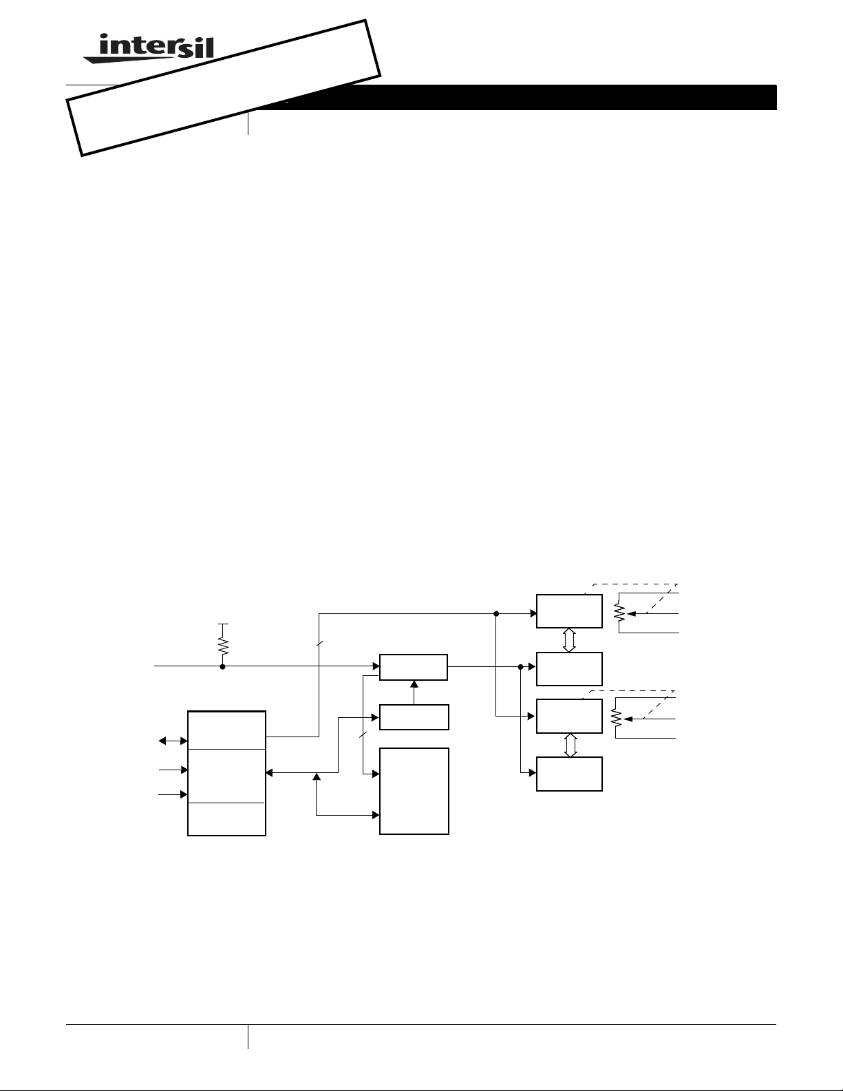
BLOCK DIAGRAM
TM
Lock
—Complies to the Gigabit Interface Converter
(GBIC) specification
—Addressable
—2.7V to 5.5V
—20 Pin TSSOP
DESCRIPTION
The X9525 combines two Digitally Controlled Potentiometers (DCP’s), and integrated EEPROM with Block
Lock™ protection. All functions of the X9525 are
accessed by an industry standard 2-Wire serial interface.
The DCP’s of the X9525 may be utilized to control the
bias and modulation currents of the laser diode in a Fiber
Optic module. The 2kbit integrated EEPROM may be
used to store module definition data.
The features of the X9525 are ideally suited to simplifying
the design of fiber optic modules which comply to the Gigabit Interface Converter (GBIC) specification. The integration of these functions into one package significantly
reduces board area, cost and increases reliability of laser
diode modules.
WP
SDA
SCL
A
R
WIPER
COUNTER
REGISTER
8
PROTECT
LOGIC
CONSTAT
DATA
REGISTER
COMMAND
DECODE &
CONTROL
o
LOGIC
THRESHOLD
RESET LOGIC
REGISTER
4
2kbit
EEPROM
ARRAY
8 - BIT
NONVOLATILE
MEMORY
WIPER
COUNTER
REGISTER
8 - BIT
NONVOLATILE
MEMORY
H1
R
W1
R
L1
R
H2
R
W2
R
L2
1
CAUTION: These devices are sensitive to electrostatic discharge; follow proper IC Handling Procedures.
1-888-INTERSIL or 1-888-468-3774
©2001 Intersil Inc., Patents Pending. Copyright Intersil Americas Inc. 2006. All Rights Reserved
| Intersil (and design) is a registered trademark of Intersil Americas Inc.
All other trademarks mentioned are the property of their respective owners.

X9525
www.BDTIC.com/Intersil
Ordering Information
PART
PART NUMBER
X9525V20I X9525VI -40 to +85 20 Ld TSSOP
X9525V20IZ X9525VZI -40 to +85 20 Ld TSSOP
*Add "T1" suffix for tape and reel.
NOTE: Intersil Pb-free plus anneal products employ special Pb-free
material sets; molding compounds/die attach materials and 100%
matte tin plate termination finish, which are RoHS compliant and
compatible with both SnPb and Pb-free soldering operations. Intersil
Pb-free products are MSL classified at Pb-free peak reflow
temperatures that meet or exceed the Pb-free requirements of
IPC/JEDEC J STD-020.
MARKING
TEMP
RANGE (°C) PACKAGE
(Pb-free)
PIN CONFIGURATION
PIN ASSIGNMENT
Pin Name Function
1
2
3
6
7WP
8SCL
9SDA
10 Vss Ground.
11
12
13
20
4, 5, 14, 15,
16, 17, 18,
19
R
R
R
R
R
R
V
H2
w2
A
W1
H1
CC
NC
L2
L1
Connection to end of resistor array for (the 256 Tap) DCP 2.
Connection to terminal equivalent to the “Wiper” of a mechanical potentiometer for DCP 2.
Connection to other end of resistor array for (the 256 Tap) DCP 2.
Physical Device Address input. A match in the slave address serial data stream, and the Physical De-
0
vice Address input pin must be in order to initiate communication with the X9525. A maximum of two
(2) devices may occupy the same 2-wire serial bus.
Write Protect Control Pin. WP pin is a TTL level compatible input. When held HIGH, Write Protection
is enabled. In the enabled state, this pin prevents all nonvolatile “write” operations. Also, when the Write
Protection is enabled, and the device Block Lock feature is active (i.e. the Block Lock bits are NOT
[0,0]), then no “write” (volatile or nonvolatile) operations can be performed in the device (including the
wiper position of any of the integrated Digitally Controlled Potentiometers (DCPs). The WP pin uses an
internal “pull-up” resistor, thus if left floating the write protection feature is enabled.
Serial Clock. This is a TTL level compatible input pin used to control the serial bus timing for data input
and output.
Serial Data. SDA is a bidirectional TTL level compatible pin used to transfer data into and out of the
device. The SDA pin input buffer is always active (not gated). This pin requires an external pull up
resistor.
Connection to other end of resistor for (the 100 Tap) DCP 1.
Connection to terminal equivalent to the “Wiper” of a mechanical potentiometer for DCP 1.
Connection to end of resistor array for (the 100 Tap) DCP 1.
Supply Voltage.
No Connect
20 Pin TSSOP
R
R
W2
R
NC
NC
WP
SCL
SDA
V
H2
L2
A
SS
1
2
3
4
5
6
0
7
8
9
10
NOT TO SCALE
20
19
18
17
16
15
14
13
12
11
VCC
NC
NC
NC
NC
NC
NC
R
H1
R
W1
R
L1
2
FN8210.1
January 3, 2006
SCL
www.BDTIC.com/Intersil
SDA
X9525
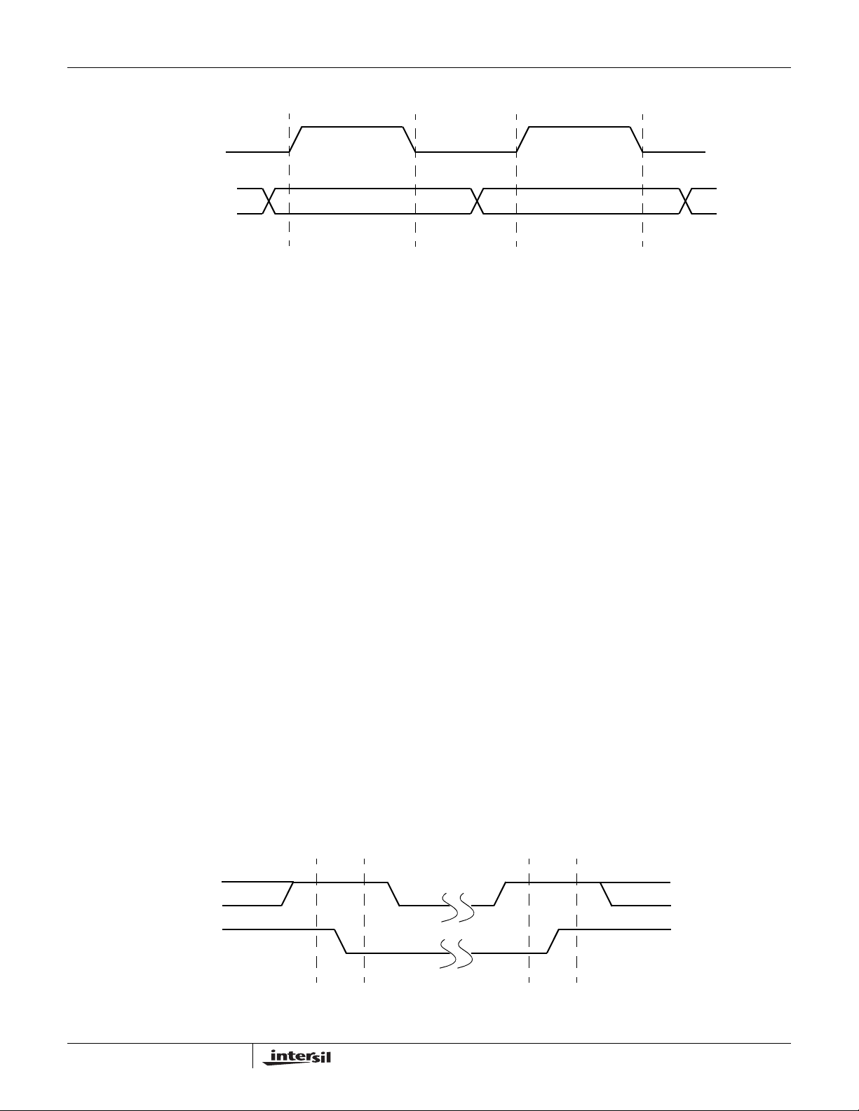
Data Stable Data Change Data Stable
Figure 1. Valid Data Changes on the SDA Bus
PRINCIPLES OF OPERATION
SERIAL INTERFACE
Serial Interface Conventions
The device supports a bidirectional bus oriented protocol.
The protocol defines any device that sends data onto the
bus as a transmitter, and the receiving device as the
receiver. The device controlling the transfer is called the
master and the device being controlled is called the
slave. The master always initiates data transfers, and
provides the clock for both transmit and receive operations. Therefore, the X9525 operates as a slave in all
applications.
Serial Clock and Data
Data states on the SDA line can change only while SCL
is LOW. SDA state changes while SCL is HIGH are
reserved for indicating START and STOP conditions.
See Figure 1. On power-up of the X9525, the SDA pin is
in the input mode.
Serial Start Condition
All commands are preceded by the START condition,
which is a HIGH to LOW transition of SDA while SCL is
HIGH. The device continuously monitors the SDA and
SCL lines for the START condition and does not respond
to any command until this condition has been met. See
Figure 2.
Serial Stop Condition
All communications must be terminated by a STOP
condition, which is a LOW to HIGH transition of SDA
while SCL is HIGH. The STOP condition is also used to
place the device into the Standby power mode after a
read sequence. A STOP condition can only be issued
after the transmitting device has released the bus. See
Figure 2.
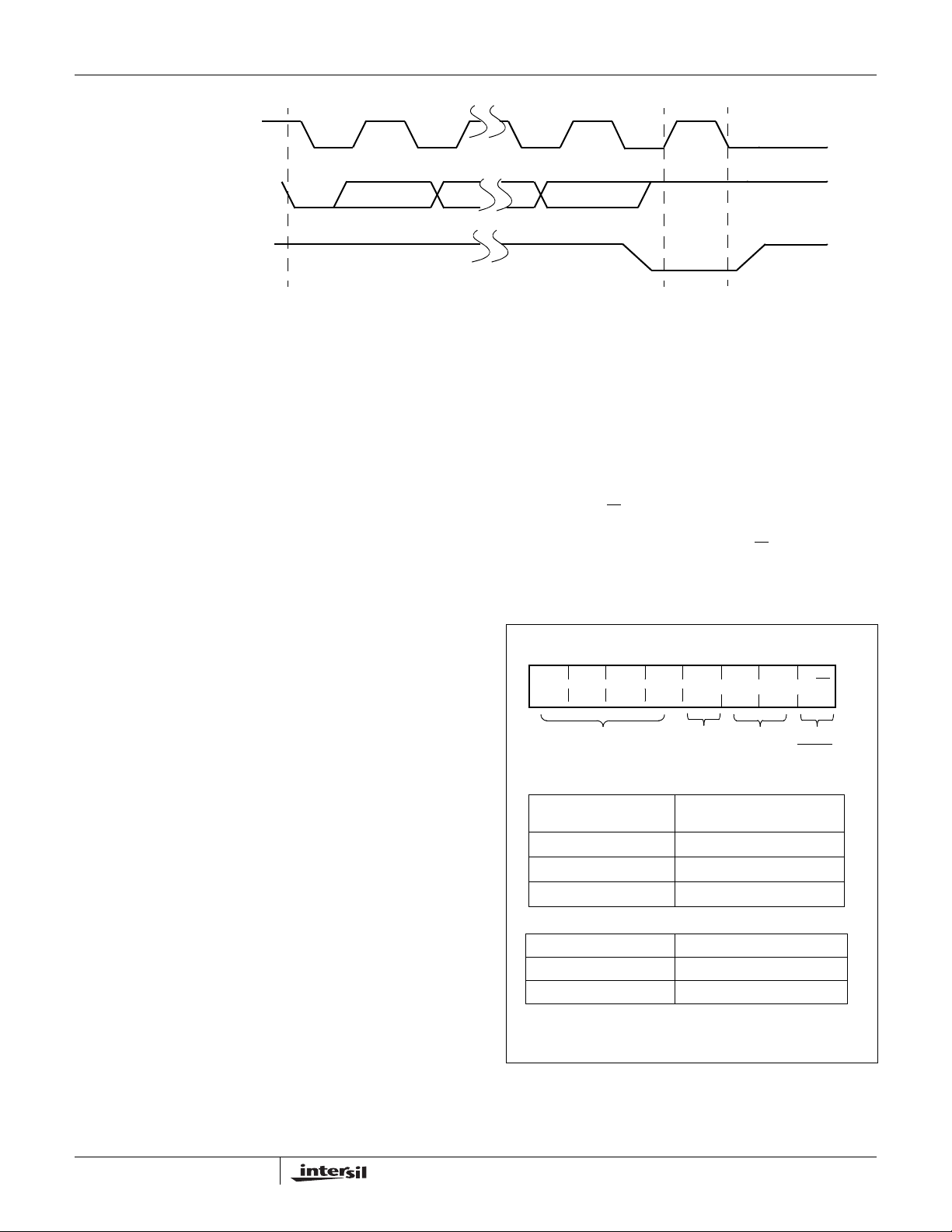
Serial Acknowledge
An ACKNOWLEDGE (ACK) is a software convention
used to indicate a successful data transfer. The transmitting device, either master or slave, will release the
bus after transmitting eight bits. During the ninth clock
cycle, the receiver will pull the SDA line LOW to
ACKNOWLEDGE that it received the eight bits of data.
Refer to Figure 3.
The device will respond with an ACKNOWLEDGE after
recognition of a START condition if the correct Device
Identifier bits are contained in the Slave Address Byte. If
a write operation is selected, the device will respond with
an ACKNOWLEDGE after the receipt of each subsequent eight bit word.
In the read mode, the device will transmit eight bits of
data, release the SDA line, then monitor the line for an
ACKNOWLEDGE. If an ACKNOWLEDGE is detected
and no STOP condition is generated by the master, the
device will continue to transmit data. The device will ter-
SCL
SDA
Start Stop
Figure 2. Valid Start and Stop Conditions
3
FN8210.1
January 3, 2006
SCL
www.BDTIC.com/Intersil
SCL
from
from
Master
Master
Data Output
from
Transmitter
Data Output
from
Receiver
X9525
81 9
Start Acknowledge
Figure 3. Acknowledge Response From Receiver
minate further data transmissions if an ACKNOWLEDGE
is not detected. The master must then issue a STOP
condition to place the device into a known state.
DEVICE INTERNAL ADDRESSING
Addressing Protocol Overview
The user addressable internal components of the X9525
can be split up into three main parts:
—Two Digitally Controlled Potentiometers (DCPs)
—EEPROM array
—Control and Status (CONSTAT) Register
Depending upon the operation to be performed on
each of these individual parts, a 1, 2 or 3 Byte protocol is used. All operations however must begin with
the Slave Address Byte being issued on the SDA pin.
The Slave address selects the part of the X9525 to
be addressed, and specifies if a Read or Write operation is to be performed.
It should be noted that in order to perform a write operation to either a DCP or the EEPROM array, the Write
Enable Latch (WEL) bit must first be set (See “BL1, BL0:
Block Lock protection bits - (Nonvolatile)” on page 12.)
Slave Address Byte
Following a START condition, the master must output a
Slave Address Byte (Refer to Figure 4.). This byte consists of four parts:
—The Device Type Identifier which consists of the most
significant four bits of the Slave Address (SA7 - SA4).
The Device Type Identifier must always be set to 1010
in order to select the X9525.
—SA3 is the Physical Device Address bit, whose logic
level must match that of the corresponding A
order to enable communication to the X9525.
0
pin in
—The next two bits (SA2 - SA1) are the Internal Device
Address bits. Setting these bits to 00 internally selects
the EEPROM array, while setting these bits to 11
selects the DCP structures in the X9525. The CONSTAT Register may be selected using the Internal
Device Address 10.
—The Least Significant Bit of the Slave Address (SA0)
Byte is the R/W
bit. This bit defines the operation to be
performed on the device being addressed (as defined
in the bits SA2 - SA1). When the R/W
bit is “1”, then a
READ operation is selected. A “0” selects a WRITE
operation (Refer to Figure 4.)
SA6SA7
SA5
1010
DEVICE TYPE
IDENTIFIER
Internal Address
(SA2 - SA1)
00
10
SA3 SA2 SA1
SA4
A
0
PHYSICAL
DEVICE
ADDRESS
Internally Addressed
EEPROM Array
CONSTAT Register
11
Bit SA0 Operation
0WRITE
1 READ
INTERNAL
DEVICE
ADDRESS
Device
DCP
SA0
R/W
READ /
WRITE
Figure 4. Slave Address Format
4
FN8210.1
January 3, 2006
Nonvolatile Write Acknowledge Polling
www.BDTIC.com/Intersil
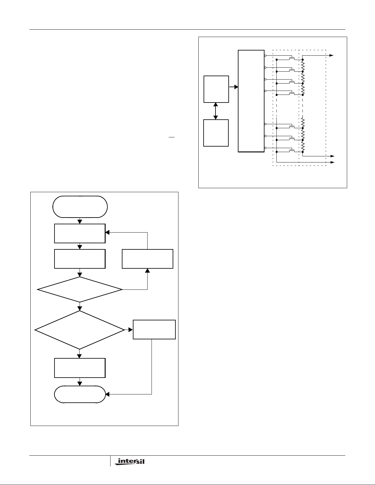
After a nonvolatile write command sequence (for either
the EEPROM array, the Non Volatile Memory of a DCP
(NVM), or the CONSTAT Register) has been correctly
issued (including the final STOP condition), the X9525
initiates an internal high voltage write cycle. This cycle
typically requires 5 ms. During this time, no further Read
or Write commands can be issued to the device. Write
Acknowledge Polling is used to determine when this high
voltage write cycle has been completed.
To perform acknowledge polling, the master issues a
START condition followed by a Slave Address Byte. The
Slave Address issued must contain a valid Internal
Device Address. The LSB of the Slave Address (R/W
can be set to either 1 or 0 in this case. If the device is still
busy with the high voltage cycle then no ACKNOWLEDGE will be returned. If the device has completed the
write operation, an ACKNOWLEDGE will be returned
and the host can then proceed with a read or write operation. (Refer to Figure 5.).
X9525
)
N
WIPER
COUNTER
REGISTER
(WCR)
NON
VOLATILE
MEMORY
(NVM)
DECODER
“WIPER”
FET
SWITCHES
2
1
0
Figure 6. DCP Internal Structure
RESISTOR
ARRAY
R
Hx
R
Lx
R
Wx
Byte load completed
by issuing STOP.
Enter ACK Polling
Issue START
Issue Slave Address
Byte (Read or Write)
ACK
returned?
YES
High Voltage Cycle
complete. Continue
command sequence?
YES
Continue normal
Read or Write
command sequence
PROCEED
DIGITALLY CONTROLLED POTENTIOMETERS
DCP Functionality
The X9525 includes two independent resistor arrays.
These arrays respectively contain 99 and 255 discrete
resistive segments that are connected in series. The
physical ends of each array are equivalent to the fixed
Issue STOP
terminals of a mechanical potentiometer (R
inputs - where x = 1,2).
At both ends of each array and between each resistor
NO
segment there is a CMOS switch connected to the wiper
) output. Within each individual array, only one
(R
x
w
switch may be turned on at any one time. These
switches are controlled by the Wiper Counter Register
(WCR) (See Figure 6). The WCR is a volatile register.
NO
Issue STOP
On power-up of the X9525, wiper position data is automatically loaded into the WCR from its associated Non
Volatile Memory (NVM) Register. The intial values of the
DCP WCR’s (before the contents of the NVM is loaded
into the WCR) are 0 and 255 for DCP1 (100 tap) and
DCP2 (256 tap) respectively. The data in the WCR is
then decoded to select and enable one of the respective
FET switches. A “make before break” sequence is used
internally for the FET switches when the wiper is moved
from one tap position to another.
and R
Hx
Lx
Figure 5. Acknowledge Polling Sequence
5
FN8210.1
January 3, 2006
Vcc
www.BDTIC.com/Intersil
X9525
Vcc (Max.)
V
TRIP
t
trans
t
pu
0
Figure 7. DCP Power-up
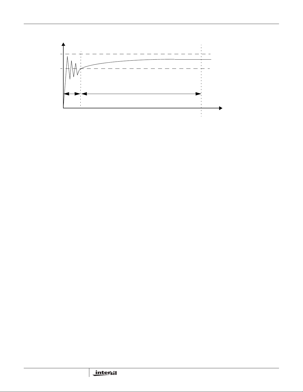
Hot Pluggability
Figure 7 shows a typical waveform that the X9525 might
experience in a Hot Pluggable situation. On power-up,
Vcc applied to the X9525 may exhibit some amount of
ringing, before it settles to the required value.
The device is designed such that the wiper terminal
) is recalled to the correct position (as per the last
(R
Wx
stored in the DCP NVM), when the voltage applied to
Vcc exceeds V
Therefore, if
settle above V
minal position is recalled by (a maximum) time:
t
. It should be noted that t
pu
tem hot plug conditions.
t
trans
for a time exceeding tpu.
TRIP
is defined as the time taken for Vcc to
(Figure 7): then the desired wiper ter-
TRIP
is determined by sys-
trans
t
trans
DCP Operations
In total there are three operations that can be performed
on any internal DCP structure:
—DCP Nonvolatile Write
—DCP Volatile Write
—DCP Read
A nonvolatile write to a DCP will change the “wiper
position” by simultaneously writing new data to the
associated WCR and NVM. Therefore, the new “wiper
position” setting is recalled into the WCR after Vcc of the
X9525 is powered down and then powered back up.
A volatile write operation to a DCP however, changes the
“wiper position” by writing new data to the associated
WCR only. The contents of the associated NVM register
remains unchanged. Therefore, when Vcc to the device
is powered down then back up, the “wiper position”
reverts to that last position written to the DCP using a
nonvolatile write operation.
t
Maximum Wiper Recall time
Both volatile and nonvolatile write operations are
executed using a three byte command sequence: (DCP)
Slave Address Byte, Instruction Byte, followed by a Data
Byte (See Figure 9).
A DCP Read operation allows the user to “read out” the
current “wiper position” of the DCP, as stored in the
associated WCR. This operation is executed using the
Random Address Read command sequence, consisting
of the (DCP) Slave Address Byte followed by an
Instruction Byte and the Slave Address Byte again (Refer
to Figure 10.).
+
Instruction Byte
While the Slave Address Byte is used to select the DCP
devices, an Instruction Byte is used to determine which
DCP is being addressed.
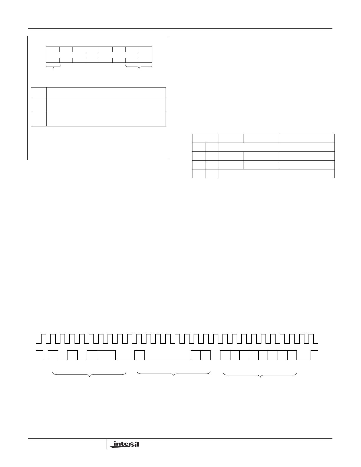
The Instruction Byte (Figure 8) is valid only when the
Device Type Identifier and the Internal Device Address
bits of the Slave Address are set to 1010A
case, the two Least Significant Bit’s (I1 - I0) of the
Instruction Byte are used to select the particular DCP
(0 - 2). In the case of a Write to any of the DCPs (i.e. the
LSB of the Slave Address is 0), the Most Significant Bit
of the Instruction Byte (I7), determines the Write Type
(WT) performed.
If WT is “1”, then a Nonvolatile Write to the DCP
In this case, the “wiper position” of the DCP is changed
by simultaneously writing new data to the associated
WCR and NVM. Therefore, the new “wiper position” setting is recalled into the WCR after Vcc of the X9525 has
been powered down then powered back up
If WT is “0” then a DCP Volatile Write is performed. This
operation changes the DCP “wiper position” by writing
new data to the associated WCR only. The contents of
11. In this
0
occurs.
6
FN8210.1
January 3, 2006
X9525
www.BDTIC.com/Intersil
I5I6I7 I4 I3 I2 I1 I0
00WT 0 0 0 P1 P0
WRITE TYPE
†
WT
Select a Volatile Write operation to be performed
0
on the DCP pointed to by bits P1 and P0
Select a Nonvolatile Write operation to be per-
1
formed on the DCP pointed to by bits P1 and P0
†
This bit has no effect when a Read operation is being performed.
Description
DCP SELECT
Figure 8. Instruction Byte Format
the associated NVM register remains unchanged. Therefore, when Vcc to the device is powered down then back
up, the “wiper position” reverts to that last written to the
DCP using a nonvolatile write operation.
DCP Write Operation
A write to DCPx (x = 1,2) can be performed using the
three byte command sequence shown in Figure 9.
In order to perform a write operation on a particular DCP,
the Write Enable Latch (WEL) bit of the CONSTAT Register must first be set (See “BL1, BL0: Block Lock protection bits - (Nonvolatile)” on page 12.)
The Slave Address Byte 1010A
Write to a DCP is to be conducted. An ACKNOWLEDGE
is returned by the X9525 after the Slave Address, if it has
been received correctly.
Next, an Instruction Byte is issued on SDA. Bits P1 and
P0 of the Instruction Byte determine which WCR is to
be written, while the WT bit determines if the Write is to
110 specifies that a
0
be volatile or nonvolatile. If the Instruction Byte format is
valid, another ACKNOWLEDGE is then returned by the
X9525.
Following the Instruction Byte, a Data Byte is issued to
the X9525 over SDA. The Data Byte contents is latched
into the WCR of the DCP on the first rising edge of the
clock signal, after the LSB of the Data Byte (D0) has
been issued on SDA (See Figure 27).
The Data Byte determines the “wiper position” (which
FET switch of the DCP resistive array is switched ON) of
the DCP. The maximum value for the Data Byte depends
upon which DCP is being addressed (see Table below).
P1-P0 DCPx # Taps Max. Data Byte
00 Reserved
0 1 x = 1 100 Refer to APPENDIX 1
1 0 x = 2 256 FFh
11 Reserved
Using a Data Byte larger than the values specified above
results in the “wiper terminal” being set to the highest tap
position. The “wiper position” does NOT roll-over to the
lowest tap position.
For DCP2 (256 Tap), the Data Byte maps one to one to
the “wiper position” of the DCP “wiper terminal”. Therefore, the Data Byte 00001111 (15
) corresponds to set-
10
ting the “wiper terminal” to tap position 15. Similarly, the
Data Byte 00011100 (28
) corresponds to setting the
10
“wiper terminal” to tap position 28. The mapping of the
Data Byte to “wiper position” data for DCP1 (100 Tap), is
shown in “APPENDIX 1” . An example of a simple C language function which “translates” between the tap position (decimal) and the Data Byte (binary) for DCP1, is
given in “APPENDIX 2” .
1010 1
S
T
A
R
T
SLAVE ADDRESS BYTE
A
0
10
A
WT 0 0 0 0 0 P1 P0 A
C
K
INSTRUCTION BYTE
C
K
Figure 9. DCP Write Command Sequence
7
D7 D6 D5 D4 D3 D2 D1 D0
DATA BYTE
S
A
T
C
O
K
P
FN8210.1
January 3, 2006
X9525
www.BDTIC.com/Intersil
S
WRITE Operation
Signals from
the Master
t
a
r
Slave
Address
Instruction
Byte
t
SDA Bus
Signals from
the Slave
101 1100
A
0
A
C
K
“Dummy” write
W
T
00 000
Figure 10. DCP Read Sequence
It should be noted that all writes to any DCP of the X9525
are random in nature. Therefore, the Data Byte of consecutive write operations to any DCP can differ by an
arbitrary number of bits. Also, setting the bits (P1 = 0,
P0 = 0) or (P1 = 1, P0 = 1) are reserved sequences, and
will result in no ACKNOWLEDGE after sending an
Instruction Byte on SDA.
The factory default setting of all “wiper position” settings
is with 00h stored in the NVM of the DCPs. This corre-
R
sponds to having the “wiper teminal”
(x = 1,2) at the
WX
“lowest” tap position, therefore, the resistance between
R
and RLX is a minimum (essentially only the Wiper
WX
Resistance,
R
).
W
DCP Read Operation
A read of DCPx (x = 1,2) can be performed using the
three byte random read command sequence shown in
Figure 10.
S
READ Operation
t
Slave
a
r
Address
Data Byte
t
P
P
1
101 1110
0
A
C
K
A
0
A
C
K
MSB
S
t
o
p
-
“-” = DON’T CARE
LSB
DCPx
x = 1
x = 2
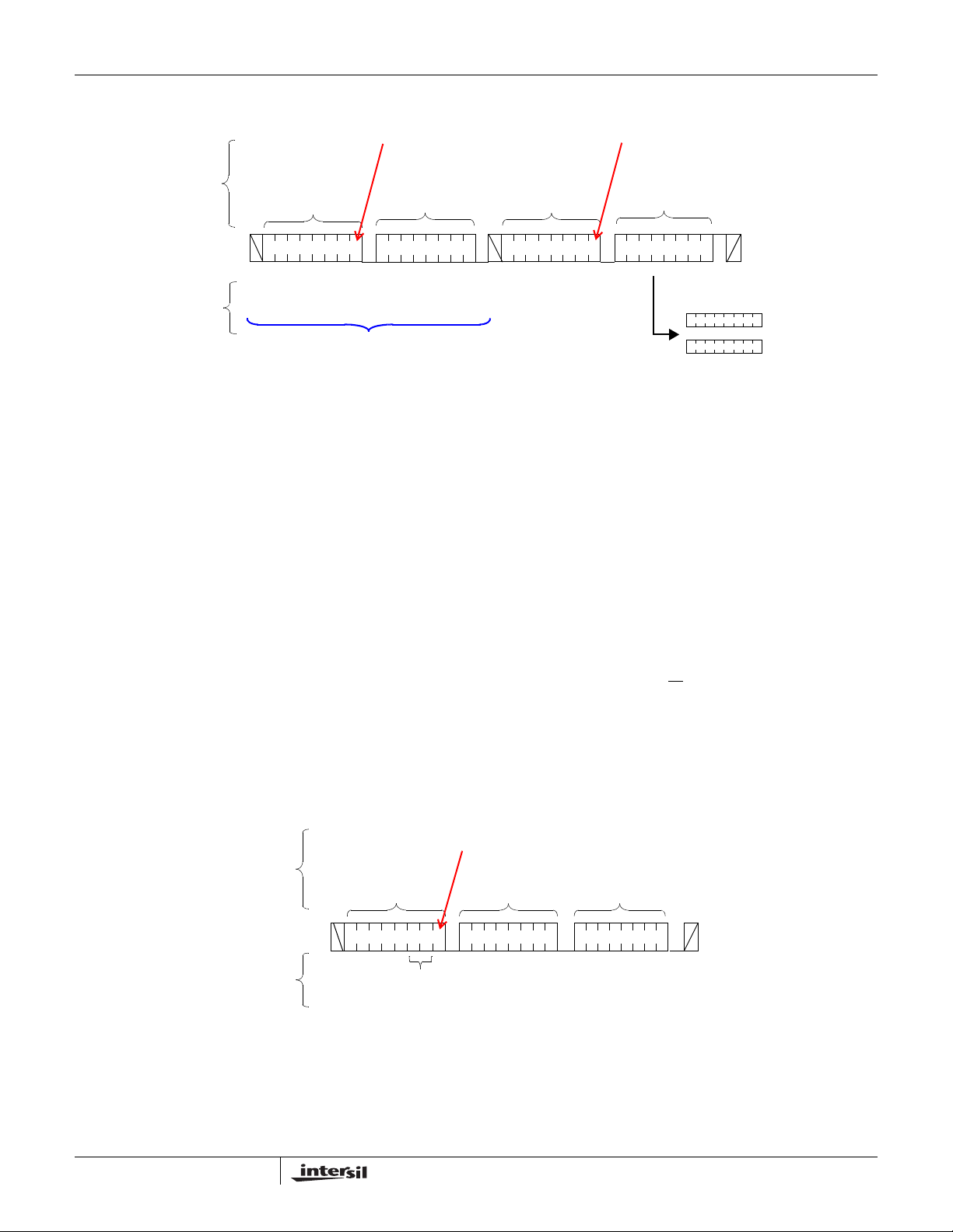
The master issues the START condition and the Slave
Address Byte 1010A
110 which specifies that a
0
“dummy” write” is to be conducted. This “dummy” write
operation sets which DCP is to be read (in the preceding
Read operation). An ACKNOWLEDGE is returned by the
X9525 after the Slave Address if received correctly. Next,
an Instruction Byte is issued on SDA. Bits P1 - P0 of the
Instruction Byte determine which DCP “wiper position” is
to be read. In this case, the state of the WT bit is “don’t
care”. If the Instruction Byte format is valid, then another
ACKNOWLEDGE is returned by the X9525.
Following this ACKNOWLEDGE, the master immediately
issues another START condition and a valid Slave
address byte with the R/W
bit set to 1. Then the X9525
issues an ACKNOWLEDGE followed by Data Byte, and
finally, the master issues a STOP condition. The Data
Byte read in this operation, corresponds to the “wiper
position” (value of the WCR) of the DCP pointed to by
bits P1 and P0.
S
Signals from
the Master
SDA Bus
Signals from
the Slave
t
a
r
t
1
Address
0100
Slave
A
0
Internal
Device
Address
WRITE Operation
Address
Byte
0
0
A
C
K
A
C
K
Figure 11. EEPROM Byte Write Sequence
8
Data
Byte
S
t
o
p
A
C
K
FN8210.1
January 3, 2006
 Loading...