

®
www.BDTIC.com/Intersil
X93255
Data Sheet February 4, 2008
Dual Digitally Controlled Potentiometers
(XDCPs™)
The Intersil X93255 is a dual digitally controlled
potentiometer (XDCP). The device consists of two resistor
arrays, wiper switches, a control section, and nonvolatile
memory. The wiper positions are controlled by individual
Up/Down interfaces.
A potentiometer is implemented by a resistor array
composed of 31 resistive elements and a wiper switching
network. The position of each wiper element is controlled by
a set of independent CS
, U/D, and INC inputs. The position
of the wiper can be stored in nonvolatile memory and then
be recalled upon a subsequent power-up operation.
Each potentiometer is connected as a two-terminal variable
resistor and can be used in a wide variety of applications
including:
• Bias and gain control
• LCD Contrast Adjustment
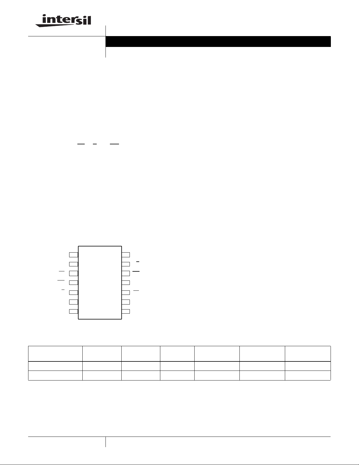
Pinout
X93255
(14 LD TSSOP)
TOP VIEW
Features
• Dual solid-state potentiometers
• Independent Up/Down interfaces
• 32 wiper tap points per potentiometer
- Wiper position stored in nonvolatile memory and
recalled on power-up
• 31 resistive elements per potentiometer
- Temperature compensated
- Maximum resistance tolerance ± 25%
- Terminal voltage, 0 to V
• Low power CMOS
-V
= 5V ± 10%
CC
- Active current, 200µA typ.
- Standby current, 4µA max
• High reliability
- Endurance 200,000 data changes per bit
- Register data retention, 100 years
TOTAL
value = 50kΩ
•R
• Package
- 14 Ld TSSOP
CC
FN8187.1
DNC*
R
L1
CS
INC
U/D
R
H2
V
SS
*Do not connect.
1
2
1
3
2
4
5
2
6
7
R
14
13
12
11
10
9
8
H1
U/D
INC
V
CC
CS
R
L2
DNC*
1
1
2
Ordering Information
TEMP
PART NUMBER PART MARKING VCC LIMITS (V) R
X93255UV14I X9325 5UVI 5 ±10% 50 -40 to +85 14 Ld TSSOP M14.173
X93255UV14IT1* X9325 5UVI 5 ±10% 50 -40 to +85 14 Ld TSSOP M14.173
* Please refer to TB347 for details on reel specifications.
TOTAL
(kΩ)
RANGE (°C) PACKAGE PKG DWG. #
1
CAUTION: These devices are sensitive to electrostatic discharge; follow proper IC Handling Procedures.
1-888-INTERSIL or1-888-468-3774
XDCP is a trademark of Intersil Americas Inc. Copyright Intersil Americas Inc. 2005, 2008. All Rights Reserved
| Intersil (and design) is a registered trademark of Intersil Americas Inc.
All other trademarks mentioned are the property of their respective owners.
Block Diagram
www.BDTIC.com/Intersil
UP/DOWN
(U/D1)
INCREMENT
(INC
DEVICE SELECT
(CS
UP/DOWN
(U/D2)
INCREMENT
(INC
DEVICE SELECT
(CS
X93255
(SUPPLY VOLTAGE)
V
CC
R
30kΩ
30kΩ
CONTROL
)
1
)
1
)
2
)
2
AND
MEMORY
CONTROL
AND
MEMORY
H1
R
L1
R
H2
R
L2
Pin Descriptions
TSSOP SYMBOL DESCRIPTION
1 DNC Do Not Connect
2R
3CS
4INC
5U/D
6R
7V
8 DNC Do Not Connect
9R
10 CS
11 V
12 INC
13 U/D
14 R
L1
H2
SS
L2
CC
H1
(GROUND)
V
SS
Low Terminal 1
1
2
2
Chip Select 1
Increment 2
Up/Down 2
High Terminal 2
Ground
Low Terminal 2
2
Chip Select 2
Supply Voltage
1
1
Increment 1
Up/Down 1
High Terminal 1
2
FN8187.1
February 4, 2008
X93255
www.BDTIC.com/Intersil
Absolute Maximum Ratings Thermal Information
Voltage on CS, INC, U/D, RH, RL and V
with respect to VSS . . . . . . . . . . . . . . . . . . . . . . . . . .-1V to +6.5V
Maximum resistor current . . . . . . . . . . . . . . . . . . . . . . . . . . . . . 2mA
CC
Recommended Operating Conditions
Temperature Range
Industrial. . . . . . . . . . . . . . . . . . . . . . . . . . . . . . . . .-40°C to +85°C
Supply Voltage
. . . . . . . . . . . . . . . . . . . . . . . . . . . . . . . . . .5V ±10% (Note 6)
V
CC
CAUTION: Do not operate at or near the maximum ratings listed for extended periods of time. Exposure to such conditions may adversely impact product reliability and
result in failures not covered by warranty.
NOTES:
1. Absolute linearity is utilized to determine actual wiper resistance vs expected resistance = (R
±1 Ml Maximum. n = 1 .. 29 only
2. Relative linearity is a measure of the error in step size between taps = R
3. 1 Ml = Minimum Increment = R
4. Typical values are for T
5. Limits established by characterization and are not production tested.
6. When performing multiple write operations, V
7. Parts are 100% tested at +25°C. Over-temperature limits established by characterization and are not production tested.
= +25°C and nominal supply voltage.
A
TOT
/31.
must not decrease by more than 150mV from its initial value.
CC
Temperature under bias. . . . . . . . . . . . . . . . . . . . . .-65°C to +135°C
Storage temperature . . . . . . . . . . . . . . . . . . . . . . . .-65°C to +150°C
Lead temperature (soldering 10s) . . . . . . . . . . . . . . . . . . . . .+300°C
Maximum reflow temperature (40s). . . . . . . . . . . . . . . . . . . .+240°C
H(n+1)
(actual) - R
H(n)
- [R
+ Ml] = ±0.5 Ml, n = 1 .. 29 only.
H(n)
(expected)) =
H(n)
Potentiometer Characteristics Over recommended operating conditions, unless otherwise specified.
MIN
SYMBOL PARAMETER TEST CONDITIONS/NOTES
R
TOT
V
R
I
C
H/CL/CW
R
W
W
End-to-End Resistance 37.5 50 62.5 kΩ
RH, RL Terminal Voltages 0 V
Power Rating R
Noise Ref: 1kHz (Note 5) -120 dBV
Wiper Resistance (Note 5) 1000 Ω
Wiper Current (Note 5) 0.6 mA
Resolution 3%
Absolute Linearity (Note 1) R
Relative Linearity (Note 2) R
Temperature Coefficient (Notes 5) ±35 ppm/°C
R
TOTAL
Potentiometer Capacitances See “Circuit #2 SPICE Macro Model”
= 50kΩ (Note 5) 1 mΩ
TOTAL
H(n)(actual)
H(n+1 - [RH(n)+MI
on page 4
- R
H(n)(expected)
] ±0.5 MI
(Note 7)
TYP
(Note 4)
10/10/25 pF
MAX
(Note 7) UNIT
CC
(Note 6)
(Note 6)
±1 MI
(Note 3)
(Note 3)
V
3
FN8187.1
February 4, 2008

X93255
www.BDTIC.com/Intersil
DC Operating Specifications
Over recommended operating conditions unless otherwise specified.
SYMBOL PARAMETER TEST CONDITIONS
I
CC1
I
CC2
I
SB
I
I
I
V
V
C
(Note 6)
Endurance and Data Retention
VCC Active Current (Increment) per DCP CS = VIL, U/D = VIL or VIH and
= 0.4V @ max. t
INC
VCC Active Current (Store)
(EEPROM Store) per DCP
CS = VIH, U/D = VIL or VIH and
INC
= V
@ max. t
IH
WR
Standby Supply Current CS = VCC - 0.3V, U/D and
=VSS or VCC - 0.3V
INC
CS VCS = V
LI
CS VCC = 5V, CS = 0
LI
INC, U/D Input Leakage Current VIN = V
LI
CS, INC, U/D Input HIGH Voltage V
IH
CS, INC, U/D Input LOW Voltage -0.5 V
IL
CS
IN
, INC, U/D Input Capacitance VCC = 5V, VIN = VSS, TA= +25°C,
f = 1MHz
CC
to V
SS
(Note 5)
CC
AC Conditions of Test
PARAMETER MIN UNIT
Minimum endurance 200,000 Data changes per bit
Data retention 100 Years
MIN
(Note 7)
TYP
(Note 4)
200 300 µA
CYC
120 200 250 µA
x 0.7 VCC + 0.5 V
CC
Input pulse levels 0V to 5V
Input rise and fall times 10ns
Input reference levels 1.5V
MAX
(Note 7) UNIT
1400 µA
4µA
±1 µA
±1 µA
x 0.1 V
CC
10 pF
Test Circuit #1 Circuit #2 SPICE Macro Model
TEST POINT
VH/R
H
R
H
10pF
R
TOTAL
C
C
H
W
25pF
C
10pF
R
L
L
AC Operating Characteristics Over recommended operating conditions unless otherwise specified. In the table, CS, INC, U/D, R
are used to refer to either CS1 or CS2, etc.
R
L
SYMBOL PARAMETER
CS to INC Setup 100 ns
Cl
INC HIGH to U/D Change 100 ns
lD
U/D to INC Setup 100 ns
DI
INC LOW Period 1 µs
lL
INC HIGH Period 1 µs
lH
INC Inactive to CS Inactive 1 µs
lC
CS Deselect Time (No store) 250 ns
CS Deselect Time (Store) 10 ms
INC Cycle Time 2 µs
INC
Input Rise and Fall Time 500 µs
t
CPH
t
CPH
t
CYC
t
R, tF
t
t
t
t
t
t
(Note 5)
t
R VCC
VCC Power-up Rate 1 50 V/ms
(Note 5)
t
WR
Store cycle 510ms
MIN
(Note 7)
TYP
(Note 4)
MAX
(Note 7) UNIT
H
and
4
FN8187.1
February 4, 2008

AC Timing
www.BDTIC.com/Intersil
CS
INC
X93255
t
CYC
t
CI
t
IL
t
IH
t
IC
(STORE)
t
CPH
90% 90%
10%
t
ID
U/D
Note: CS, INC, U/D, RH and RL are used to refer
to either CS
or CS2, etc.
1
t
DI
Power-up and Power-down Requirements
There are no restrictions on the power-up or power-down
conditions of V
potentiometer pins provided that V
positive than or equal to V
V
ramp rate specification is always in effect.
CC
and the voltages applied to the
CC
and VL, i.e., VCC ≥ VH,VL. The
H
is always more
CC
Pin Descriptions
RH and R
The R
terminals of a variable resistor. The minimum voltage is V
and the maximum is V
references the relative position of the terminal in relation to
wiper movement direction selected by the U/D
potentiometer.
Up/Down (U/D)
The U/D input controls the direction of a single
potentiometer’s wiper movement and whether the counter is
incremented or decremented.
Increment (INC)
The INC input is negative-edge triggered. Toggling INC will
move the wiper and either increment or decrement the
pertaining potentiometer’s counter in the direction indicated
by the logic level on the pertaining potentiometer’s U/D
input.
Chip Select (CS)
A potentiometer is selected when the pertaining CS input is
LOW. Its current counter value is stored in nonvolatile
memory when the pertaining CS
pertaining INC
is complete, the affected potentiometer will be placed in the
low power standby mode until the potentiometer is selected
once again.
L
and RL pins of the X93255 are equivalent to the end
H
. The terminology of RH and R
CC
input per
is returned HIGH while the
input is also HIGH. After the store operation
SS
L
t
F
t
R
Principles of Operation
There are multiple sections for each potentiometer in the
X93255: an input control, a counter and decode section; the
nonvolatile memory; and a resistor array. Each input control
section operates just like an up/down counter. The output of
this counter is decoded to turn on a single electronic switch
connecting a point on the resistor array to the wiper output.
Under the proper conditions, the contents of the counter can
be stored in nonvolatile memory and retained for future use.
Each resistor array is comprised of 31 individual resistors
connected in series. At either end of the array and between
each resistor is an electronic switch that transfers the
connection at that point to the wiper. The wiper is connected
to the R
terminal, forming a variable resistor from RH to RL.
L
Each wiper, when at either fixed terminal, acts like its
mechanical equivalent and does not move beyond the last
position. That is, the counter does not wrap around when
clocked to either extreme.
If the wiper is moved several positions, multiple taps are
connected to the wiper for up to 10µs. The 2-terminal
resistance value for the device can temporarily change by a
significant amount if the wiper is moved several positions.
When the device is powered-down, the last wiper position
stored will be maintained in the nonvolatile memory for each
potentiometer. When power is restored, the contents of the
memory are recalled and each wiper is set to the value last
stored.
5
FN8187.1
February 4, 2008

X93255
www.BDTIC.com/Intersil
Instructions and Programming
The INC, U/D and CS inputs control the movement of the
pertaining wiper along the resistor array. With CS
the pertaining potentiometer is selected and enabled to
respond to the U/D
on INC
will increment or decrement (depending on the state
of the U/D
input) a 5-bit counter. The output of this counter is
and INC inputs. HIGH to LOW transitions
decoded to select one of thirty two wiper positions along the
resistive array.
The value of the counter is stored in nonvolatile memory
whenever each CS
INC
input is also HIGH. In order to avoid an accidental store
during power-up, each CS
transitions HIGH while the pertaining
must go HIGH with VCC during
initial power-up. When left open, each CS
pulled up to V
by an internal 30k resistor.
CC
The system may select the X93255, move any wiper and
deselect the device without having to store the latest wiper
position in nonvolatile memory. After the wiper movement is
performed as previously described and once the new
position is reached, the system must keep INC
taking CS
HIGH. The new wiper position will be maintained
until changed by the system or until a power-up/down cycle
recalled the previously stored data. In order to recall the
stored position of the wiper on po wer-up, the CS
held HIGH.
This procedure allows the system to always power-up to a
preset value stored in nonvolatile memory; then during
system operation minor adjustments could be made. The
adjustments might be based on user preference, system
parameter changes due to temperature drift, or other system
trim requirements.
set LOW,
pin is internally
LOW while
pin must be
Mode Selection
CS INC U/D MODE
L H Wiper Up
L L Wiper Down
H X Store Wiper Position
H X X Standby Current
L X No Store, Return to Standby
L H Wiper Up (not recommended)
L L Wiper Down (not recommended)
Symbol Table
WAVEFORM INPUTS OUTPUTS
Must be
steady
May change
from Low to
High
May change
from High to
Low
Don’t Care:
Changes
Allowed
N/A Center Line
Will be
steady
Will change
from Low to
High
Will change
from High to
Low
Changing:
State Not
Known
is High
Impedance
The state of U/D
may be changed while CS remains LOW.
This allows the host system to enable the device and then
move each wiper up and down until the proper trim is
attained.
6
FN8187.1
February 4, 2008

X93255
www.BDTIC.com/Intersil
Thin Shrink Small Outline Plastic Packages (TSSOP)
N
INDEX
AREA
123
0.05(0.002)
-AD
e
b
0.10(0.004) C AM BS
NOTES:
1. These package dimensions are within allowable dimensions of
JEDEC MO-153-AC, Issue E.
2. Dimensioning and tolerancing per ANSI Y14.5M-1982.
3. Dimension “D” does not include mold flash, protrusions or gate burrs.
Mold flash, protrusion and gate burrs shall not exceed 0.15mm
(0.006 inch) per side.
4. Dimension “E1” does not include interlead flash or protrusions. Interlead flash and protrusions shall not exceed 0.15mm (0.006 inch) per
side.
5. The chamfer on the body is optional. If it is not present, a visual index
feature must be located within the crosshatched area.
6. “L” is the length of terminal for soldering to a substrate.
7. “N” is the number of terminal positions.
8. Terminal numbers are shown for reference only.
9. Dimension “b” does not include dambar protrusion. Allowable dambar
protrusion shall be 0.08mm (0.003 inch) total in excess of “b” dimension at maximum material condition. Minimum space between protrusion and adjacent lead is 0.07mm (0.0027 inch).
10. Controlling dimension: MILLIMETER. Converted inch dimensions
are not necessarily exact. (Angles in degrees)
E1
-B-
SEATING PLANE
A
-C-
M
0.25(0.010) BM M
E
α
A1
0.10(0.004)
GAUGE
PLANE
0.25
0.010
A2
L
c
M14.173
14 LEAD THIN SHRINK SMALL OUTLINE PLASTIC
PACKAGE
INCHES MILLIMETERS
SYMBOL
A - 0.047 - 1.20 -
A1 0.002 0.006 0.05 0.15 -
A2 0.031 0.041 0.80 1.05 -
b 0.0075 0.0118 0.19 0.30 9
c 0.0035 0.0079 0.09 0.20 -
D 0.195 0.199 4.95 5.05 3
E1 0.169 0.177 4.30 4.50 4
e 0.026 BSC 0.65 BSC -
E 0.246 0.256 6.25 6.50 -
L 0.0177 0.0295 0.45 0.75 6
N14 147
o
α
0
o
8
o
0
o
8
NOTESMIN MAX MIN MAX
-
Rev. 2 4/06
All Intersil U.S. products are manufactured, assembled and tested utilizing ISO9000 quality systems.
Intersil Corporation’s quality certifications can be viewed at www.intersil.com/design/quality
Intersil products are sold by description only. Intersil Corporation reserves the right to make changes in circuit design, software and/or specifications at any time without
notice. Accordingly, the reader is cautioned to verify that data sheets are current before placing orders. Information furnished by Intersil is believed to be accurate and
reliable. However, no responsibility is assumed by Intersil or its subsidiaries for its use; nor for any infringements of patents or other rights of third parties which may result
from its use. No license is granted by implic atio n or other wise u nde r any p a tent or patent rights of Intersil or its sub sidi aries.
For information regarding Intersil Corporation and its products, see www.intersil.com
7
FN8187.1
February 4, 2008
 Loading...