®
www.BDTIC.com/Intersil
X93254
Data Sheet February 4, 2008
Dual Digitally Controlled Potentiometers
(XDCPs™)
The Intersil X93254 is a dual digitally controlled
potentiometer (XDCP). The device consists of two resistor
arrays, wiper switches, a control section, and nonvolatile
memory. The wiper positions are controlled by individual
Up/Down interfaces.
A potentiometer is implemented by a resistor array
composed of 31 resistive elements and a wiper switching
network. The position of each wiper element is controlled by
a set of independent CS
, U/D, and INC inputs. The position
of the wiper can be stored in nonvolatile memory and then
be recalled upon during a subsequent power-up operation.
Each potentiometer is connected as a two-terminal variable
resistor and can be used in a wide variety of applications
including:
• Bias and Gain control
• LCD Contrast Adjustment
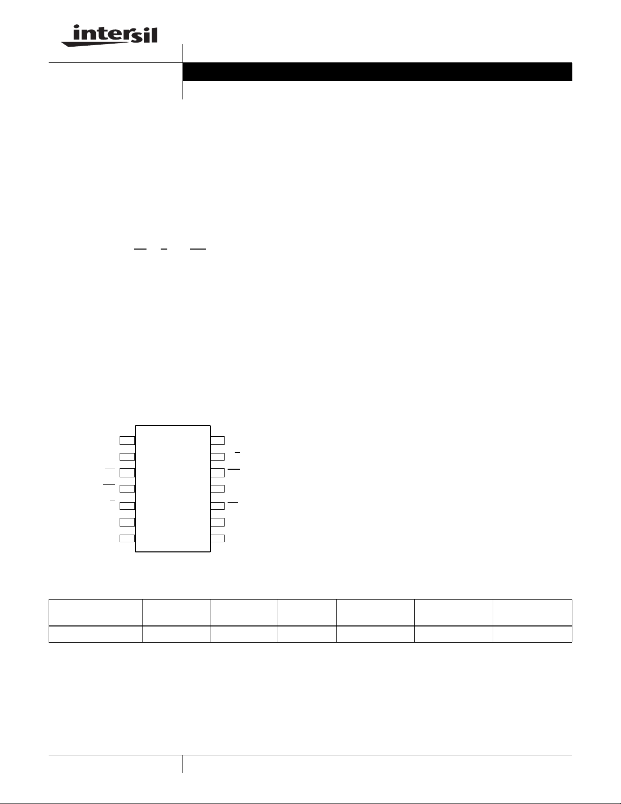
Pinout
X93254
(14 LD TSSOP)
TOP VIEW
Features
• Dual solid-state potentiometers
• Independent Up/Down interfaces
• 32 wiper tap points per potentiometer
- Wiper position stored in nonvolatile memory and
recalled on power-up
• 31 resistive elements per potentiometer
- Temperature compensated
- Maximum resistance tolerance of ± 30%
- Terminal voltage, 0 to V
• Low power CMOS
-V
= 3V ±10%
CC
- Active current, 250µA max
- Standby current, 1µA max
• High reliability
- Endurance 200,000 data changes per bit
- Register data retention, 100 years
TOTAL
value = 50kΩ
•R
• 14 Ld TSSOP package
CC
FN8186.1
DNC*
R
CS
INC
U/D
R
V
*Do not connect.
L1
H2
SS
1
2
1
3
2
4
5
2
6
7
14
13
12
11
10
R
H1
U/D
1
INC
1
V
CC
CS
2
R
9
8
L2
DNC*
Ordering Information
PART NUMBER PART MARKING VCC LIMITS (V) R
X93254UV141-3 X9325 4UVE 3 ±10% 50 -40 to +85 14 Ld TSSOP M14.173
TOTAL
(kΩ)
TEMP
RANGE (°C) PACKAGE PKG DWG. #
1
CAUTION: These devices are sensitive to electrostatic discharge; follow proper IC Handling Procedures.
1-888-INTERSIL or1-888-468-3774
XDCP is a trademark of Intersil Americas Inc. Copyright Intersil Americas Inc. 2005, 2008. All Rights Reserved
| Intersil (and design) is a registered trademark of Intersil Americas Inc.
All other trademarks mentioned are the property of their respective owners.

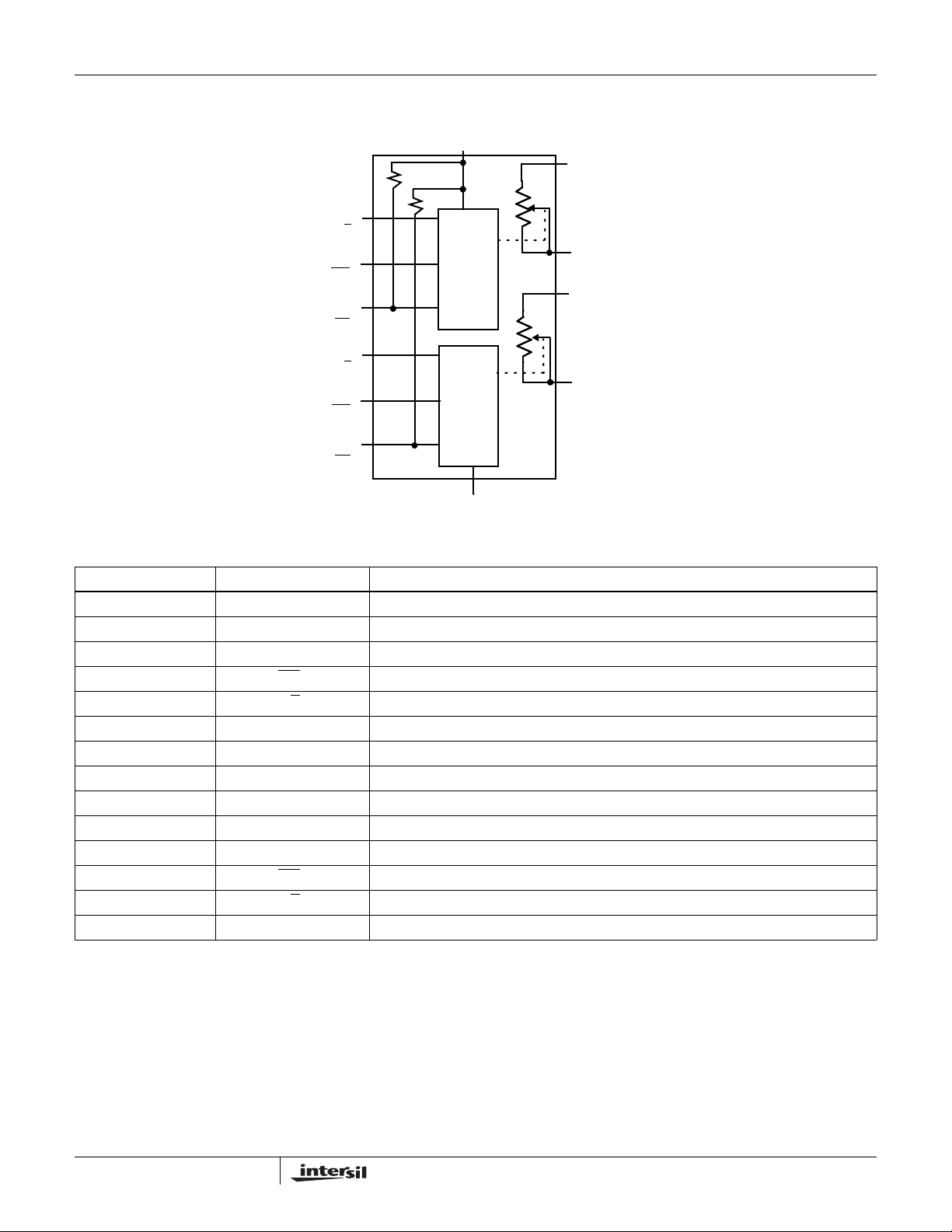
Block Diagram
www.BDTIC.com/Intersil
UP/DOWN
(U/D1)
INCREMENT
(INC
DEVICE SELECT
(CS
UP/DOWN
(U/D2)
INCREMENT
(INC
DEVICE SELECT
(CS
X93254
(SUPPLY VOLTAGE)
V
CC
R
30k
30k
CONTROL
)
1
)
1
)
2
)
2
AND
MEMORY
CONTROL
AND
MEMORY
V
(Ground)
SS
H1
R
L1
R
H2
R
L2
Pin Descriptions
TSSOP SYMBOL DESCRIPTION
1 DNC Do Not Connect
2R
3CS
4INC
5U/D
6R
7V
8 DNC Do Not Connect
9R
10 CS
11 V
12 INC
13 U/D
14 R
L1
H2
SS
L2
CC
H1
Low Terminal 1
1
2
2
Chip Select 1
Increment 2
Up/Down 2
High Terminal 2
Ground
Low Terminal 2
2
Chip Select 2
Supply Voltage
1
1
Increment 1
Up/Down 1
High Terminal 1
2
FN8186.1
February 4, 2008

X93254
www.BDTIC.com/Intersil
Absolute Maximum Ratings Thermal Information
Voltage on CS, INC, U/D, RH, RL and V
with respect to VSS . . . . . . . . . . . . . . . . . . . . . . . . . .-1V to +6.5V
Maximum resistor current . . . . . . . . . . . . . . . . . . . . . . . . . . . . . 2mA
CC
Recommended Operating Conditions
Temperature Range
Industrial. . . . . . . . . . . . . . . . . . . . . . . . . . . . . . . . .-40°C to +85°C
Supply Voltage
. . . . . . . . . . . . . . . . . . . . . . . . . . . . . . . . . .3V ±10% (Note 6)
V
CC
CAUTION: Do not operate at or near the maximum ratings listed for extended periods of time. Exposure to such conditions may adversely impact product reliability and
result in failures not covered by warranty.
NOTES:
1. Absolute linearity is utilized to determine actual wiper voltage versus expected voltage = (V
n = 1 .. 29 only
2. Relative linearity is a measure of the error in step size between taps = V
3. 1 Ml = Minimum Increment = R
4. Typical values are for T
5. Limits established by characterization and are not production tested.
6. When performing multiple write operations, V
7. Parts are 100% tested at +25°C. Over-temperature limits established by characterization and are not production tested.
= +25°C and nominal supply voltage.
A
TOT
/31.
must not decrease by more than 150mV from its initial value.
CC
Temperature under bias. . . . . . . . . . . . . . . . . . . . . .-65°C to +135°C
Storage temperature . . . . . . . . . . . . . . . . . . . . . . . .-65°C to +150°C
Lead temperature (soldering 10s) . . . . . . . . . . . . . . . . . . . . .+300°C
Maximum reflow temperature (40s). . . . . . . . . . . . . . . . . . . .+240°C
H(n+1)
- [V
(actual) - V
H(n)
+ Ml] = ±0.5 Ml, n = 1 .. 29 only.
H(n)
(expected)) = ±1 Ml Maximum.
H(n)
Potentiometer Specifications Over recommended operating conditions, unless otherwise stated.
MIN
SYMBOL PARAMETER TEST CONDITIONS/NOTES
R
TOT
V
R
I
W
C
H/CL/CW
R
W
End-to-End Resistance 37.5 50 62.5 kΩ
RH, RL Terminal Voltages 0 V
Power Rating R
Noise Ref: 1kHz -120 dBV
Wiper Resistance (Note 5) 1000 Ω
Wiper Current (Note 5) 0.6 mA
Resolution 3%
Absolute Linearity
Relative Linearity
Temperature Coefficient (Note 5) ±35 ppm/°C
R
TOTAL
Potentiometer Capacitances See “Circuit #2 SPICE Macro
(Note 1) V
(Note 2) V
= 50kΩ 1mΩ
TOTAL
- [V
H(n)+MI
- V
H(n)(expected)
H(n)(actual)
H(n+1)
Model” on page 4
(Note 7)
TYP
(Note 4)
10/10/25 pF
MAX
(Note 7) UNIT
CC
(Note 5)
(Note 5)
±1 MI
(Note 3)
±0.5 MI
(Note 3)
(Note 5)
V
3
FN8186.1
February 4, 2008
 Loading...