

®
www.BDTIC.com/Intersil
X9317
Low Noise, Low Power, 100 Taps
Data Sheet June 25, 2008
Digitally Controlled Potentiometer
(XDCP™)
The Intersil X9317 is a digitally controlled potentiometer
(XDCP™). The device consists of a resistor array, wiper
switches, a control section, and nonvolatile memory. The
wiper position is controlled by a 3-wire interface.
The potentiometer is implemented by a resistor array
composed of 99 resistive elements and a wiper switching
network. Between each element and at either end are tap
points accessible to the wiper terminal. The position of the
wiper element is controlled by the CS
, U/D, and INC inputs.
The position of the wiper can be stored in nonvolatile
memory and then be recalled upon a subsequent power-up
operation.
The device can be used as a three-terminal potentiometer
for voltage control or as a two-terminal variable resistor for
current control in a wide variety of applications.
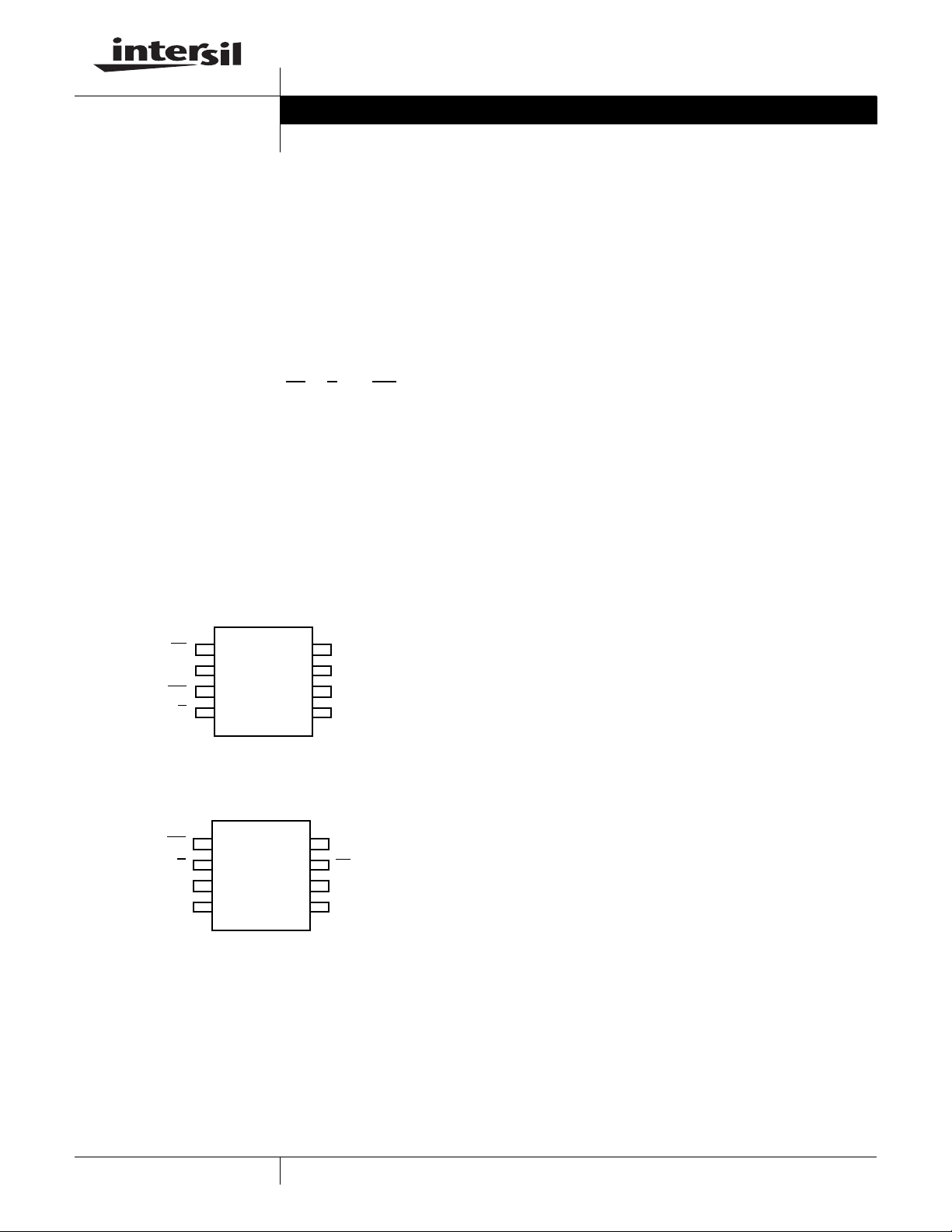
Pinouts
X9317
(8 LD TSSOP)
TOP VIEW
FN8183.4
Features
• Solid-State Potentiometer
• 3-Wire Serial Up/Down Interface
• 100 Wiper Tap Points
- Wiper Position Stored in Nonvolatile Memory and
Recalled on Power-up
• 99 Resistive Elements
- Temperature Compensated
- End-to-end Resistance Range ±20%
• Low Power CMOS
= 2.7V to 5.5V, and 5V ±10%
-V
CC
- Standby Current <1µA
• High Reliability
- Endurance, 100,000 Data Changes per Bit
- Register Data Retention, 100 years
•R
• Packages
- 8 Ld SOIC, PDIP, TSSOP, and MSOP
• Pb-Free Available (RoHS Compliant)
Values = 1kΩ, 10kΩ, 50kΩ, 100kΩ
TOTAL
CS
V
CC
INC
U/D
(8 LD PDIP, 8 LD SOIC, 8 LD MSOP)
INC
U/D
R
V
SS
1
2
X9317
3
4
X9317
TOP VIEW
1
2
X9317
3
H
4
R
8
L
R
7
W
V
SS
6
R
H
5
V
8
CC
CS
7
R
L
6
R
W
5
Applications
• LCD Bias Control
• DC Bias Adjustment
• Gain and Offset Trim
• Laser Diode Bias Control
• Voltage Regulator Output Control
1
XDCP is a trademark of Intersil Americas, Inc. Copyright Intersil Americas Inc. 2004-2005, 2008. All Rights Reserved
CAUTION: These devices are sensitive to electrostatic discharge; follow proper IC Handling Procedures.
1-888-INTERSIL or 1-888-468-3774
| Intersil (and design) is a registered trademark of Intersil Americas Inc.
All other trademarks mentioned are the property of their respective owners.
X9317
www.BDTIC.com/Intersil
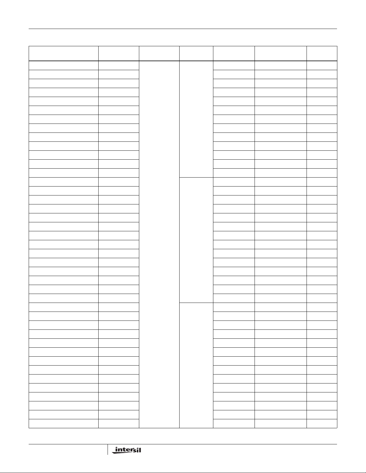
Ordering Information
LIMITS
V
CC
PART NUMBER PART MARKING
X9317ZM8* AFG 5 ±10% 1 0 to +70 8 Ld MSOP M8.118
X9317ZM8Z* (Note) DDA 0 to +70 8 Ld MSOP (Pb-free) M8.118
X9317ZM8I* AFI -40 to +85 8 Ld MSOP M8.118
X9317ZM8IZ* (Note) DCY -40 to +85 8 Ld MSOP (Pb-free) M8.118
X9317ZP X9317ZP 0 to +70 8 Ld PDIP MDP0031
X9317ZS8* X9317Z 0 to +70 8 Ld SOIC MDP0027
X9317ZS8Z* (Note) X9317Z Z 0 to +70 8 Ld SOIC (Pb-free) MDP0027
X9317ZS8I* X9317Z I -40 to +85 8 Ld SOIC MDP0027
X9317ZS8IZ* (Note) X9317Z Z I -40 to +85 8 Ld SOIC (Pb-free) MDP0027
X9317ZV8* 9317Z 0 to +70 8 Ld TSSOP M8.173
X9317ZV8Z* (Note) 9317Z Z 0 to +70 8 Ld TSSOP (Pb-free) M8.173
X9317ZV8I* 317Z I -40 to +85 8 Ld TSSOP M8.173
X9317ZV8IZ* (Note) 9317Z IZ -40 to +85 8 Ld TSSOP (Pb-free) M8.173
X9317WM8* ABF 10 0 to +70 8 Ld MSOP M8.118
X9317WM8Z* (Note) DCW 0 to +70 8 Ld MSOP (Pb-free) M8.118
X9317WM8I* ADS -40 to +85 8 Ld MSOP M8.118
X9317WM8IZ* (Note) DCT -40 to +85 8 Ld MSOP (Pb-free) M8.118
X9317WP X9317WP 0 to +70 8 Ld PDIP MDP0031
X9317WPI X9317WP I -40 to +85 8 Ld PDIP MDP0031
X9317WS8* X9317W 0 to +70 8 Ld SOIC MDP0027
X9317WS8Z* (Note) X9317W Z 0 to +70 8 Ld SOIC (Pb-free) MDP0027
X9317WS8I* X9317W I -40 to +85 8 Ld SOIC MDP0027
X9317WS8IZ* (Note) X9317W ZI -40 to +85 8 Ld SOIC (Pb-free) MDP0027
X9317WV8*, ** 9317W 0 to +70 8 Ld TSSOP M8.173
X9317WV8Z* (Note) 9317W Z 0 to +70 8 Ld TSSOP (Pb-free) M8.173
X9317WV8I* 317W I -40 to +85 8 Ld TSSOP M8.173
X9317WV8IZ* (Note) 9317W IZ -40 to +85 8 Ld TSSOP (Pb-free) M8.173
X9317UM8* AEC 50 0 to +70 8 Ld MSOP M8.118
X9317UM8Z* (Note) DCS 0 to +70 8 Ld MSOP (Pb-free) M8.118
X9317UM8I* AFE -40 to +85 8 Ld MSOP M8.118
X9317UM8IZ* (Note) DCR -40 to +85 8 Ld MSOP (Pb-free) M8.118
X9317UP X9317UP 0 to +70 8 Ld PDIP MDP0031
X9317UPI X9317UP I -40 to +85 8 Ld PDIP MDP0031
X9317US8* X9317U 0 to +70 8 Ld SOIC MDP0027
X9317US8Z* (Note) X9317U Z 0 to +70 8 Ld SOIC (Pb-free) MDP0027
X9317US8I* X9317U I -40 to +85 8 Ld SOIC MDP0027
X9317US8IZ* (Note) X9317U ZI -40 to +85 8 Ld SOIC (Pb-free) MDP0027
X9317UV8* 9317U 0 to +70 8 Ld TSSOP M8.173
X9317UV8Z* (Note) 9317U Z 0 to +70 8 Ld TSSOP (Pb-free) M8.173
X9317UV8I* 317U I -40 to +85 8 Ld TSSOP M8.173
X9317UV8IZ* (Note) 9317U IZ -40 to +85 8 Ld TSSOP (Pb-free) M8.173
(V)
R
TOTAL
(kΩ)
TEMPERATURE
RANGE (°C) PACKAGE
PKG.
DWG. #
2
FN8183.4
June 25, 2008
X9317
www.BDTIC.com/Intersil
Ordering Information (Continued)
V
LIMITS
PART NUMBER PART MARKING
X9317TM8*, ** AGD 5 ±10% 100 0 to +70 8 Ld MSOP M8.118
X9317TM8Z* (Note) DCN 0 to +70 8 Ld MSOP (Pb-free) M8.118
X9317TM8I*, ** AGF -40 to +85 8 Ld MSOP M8.118
X9317TM8IZ* (Note) DCL -40 to +85 8 Ld MSOP (Pb-free) M8.118
X9317TP X9317TP 0 to +70 8 Ld PDIP MDP0031
X9317TPI X9317TP I -40 to +85 8 Ld PDIP MDP0031
X9317TS8 X9317T 0 to +70 8 Ld SOIC MDP0027
X9317TS8Z (Note) X9317T Z 0 to +70 8 Ld SOIC (Pb-free) MDP0027
X9317TS8I X9317T I -40 to +85 8 Ld SOIC MDP0027
X9317TS8IZ (Note) X9317T ZI -40 to +85 8 Ld SOIC (Pb-free) MDP0027
X9317TV8*, ** 9317T 0 to +70 8 Ld TSSOP M8.173
X9317TV8Z* (Note) 9317T Z 0 to +70 8 Ld TSSOP (Pb-free) M8.173
X9317TV8I*, ** 317T I -40 to +85 8 Ld TSSOP M8.173
X9317TV8IZ* (Note) 9317T IZ -40 to +85 8 Ld TSSOP (Pb-free) M8.173
X9317ZM8-2.7* AFH 2.7 to 5.5 1 0 to +70 8 Ld MSOP M8.118
X9317ZM8Z-2.7* (Note) AOA 0 to +70 8 Ld MSOP (Pb-free) M8.118
X9317ZM8I-2.7* AFJ -40 to +85 8 Ld MSOP M8.118
X9317ZM8IZ-2.7* (Note) DCZ -40 to +85 8 Ld MSOP (Pb-free) M8.118
X9317ZS8-2.7* X9317Z F 0 to +70 8 Ld SOIC MDP0027
X9317ZS8Z-2.7* (Note) X9317Z ZF 0 to +70 8 Ld SOIC (Pb-free) MDP0027
X9317ZS8I-2.7* X9317Z G -40 to +85 8 Ld SOIC MDP0027
X9317ZS8IZ-2.7* (Note) X9317Z ZG -40 to +85 8 Ld SOIC (Pb-free) MDP0027
X9317ZV8-2.7* 317Z F 0 to +70 8 Ld TSSOP M8.173
X9317ZV8Z-2.7* (Note) 9317Z FZ 0 to +70 8 Ld TSSOP (Pb-free) M8.173
X9317ZV8I-2.7*, ** 317Z G -40 to +85 8 Ld TSSOP M8.173
X9317ZV8IZ-2.7* (Note) 9317Z GZ -40 to +85 8 Ld TSSOP (Pb-free) M8.173
X9317WM8-2.7* ACZ 10 0 to +70 8 Ld MSOP M8.118
X9317WM8Z-2.7* (Note) DCX 0 to +70 8 Ld MSOP (Pb-free) M8.118
X9317WM8I-2.7* ADT -40 to +85 8 Ld MSOP M8.118
X9317WM8IZ-2.7* DCU -40 to +85 8 Ld MSOP (Pb-free) M8.118
X9317WP-2.7 X9317WP F 0 to +70 8 Ld PDIP MDP0031
X9317WPI-2.7 X9317WP G -40 to +85 8 Ld PDIP MDP0031
X9317WS8-2.7* X9317W F 0 to +70 8 Ld SOIC MDP0027
X9317WS8Z-2.7* (Note) X9317W ZF 0 to +70 8 Ld SOIC (Pb-free) MDP0027
X9317WS8I-2.7*, ** X9317W G -40 to +85 8 Ld SOIC MDP0027
X9317WS8IZ-2.7*
X9317WV8-2.7* 317W F 0 to +70 8 Ld TSSOP M8.173
X9317WV8Z-2.7*
X9317WV8I-2.7*, ** 317W G -40 to +85 8 Ld TSSOP M8.173
X9317WV8IZ-2.7* (Note) AKZ -40 to +85 8 Ld TSSOP (Pb-free) M8.173
(Note) X9317W ZG -40 to +85 8 Ld SOIC (Pb-free) MDP0027
(Note) 9317W FZ 0 to +70 8 Ld TSSOP (Pb-free) M8.173
CC
(V)
R
TOTAL
(kΩ)
TEMPERATURE
RANGE (°C) PACKAGE
PKG.
DWG. #
3
FN8183.4
June 25, 2008
X9317
www.BDTIC.com/Intersil
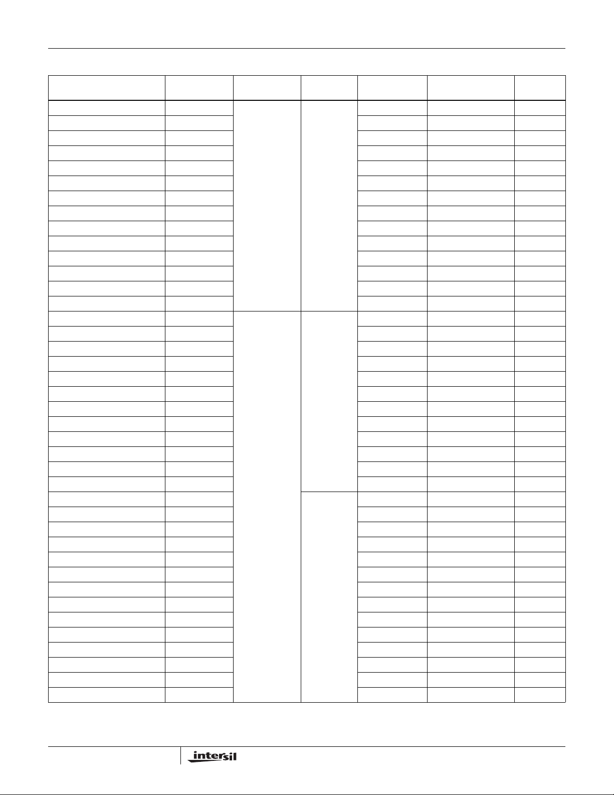
Ordering Information (Continued)
V
LIMITS
PART NUMBER PART MARKING
X9317UM8-2.7* AED 2.7 to 5.5 10 0 to +70 8 Ld MSOP M8.118
X9317UM8Z-2.7* (Note) AOB 0 to +70 8 Ld MSOP (Pb-free) M8.118
X9317UM8I-2.7*, ** AFF -40 to +85 8 Ld MSOP M8.118
X9317UM8IZ-2.7* (Note) AOH -40 to +85 8 Ld MSOP (Pb-free) M8.118
X9317US8-2.7* X9317U F 50 0 to +70 8 Ld SOIC MDP0027
X9317UP-2.7 X9317UP F 0 to +70 8 Ld PDIP MDP0031
X9317UPI-2.7 X9317UP G -40 to +85 8 Ld PDIP MDP0031
X9317US8Z-2.7* (Note) X9317U ZF 0 to +70 8 Ld SOIC (Pb-free) MDP0027
X9317US8I-2.7*, ** X9317U G -40 to +85 8 Ld SOIC MDP0027
X9317US8IZ-2.7* (Note) X9317U ZG -40 to +85 8 Ld SOIC (Pb-free) MDP0027
X9317UV8-2.7* 317U F 0 to +70 8 Ld TSSOP M8.173
X9317UV8Z-2.7* (Note) 9317U FZ 0 to +70 8 Ld TSSOP (Pb-free) M8.173
X9317UV8I-2.7*, ** 317U G -40 to +85 8 Ld TSSOP M8.173
X9317UV8IZ-2.7* (Note) 9317U GZ -40 to +85 8 Ld TSSOP (Pb-free) M8.173
X9317TM8-2.7*, ** AGE 100 0 to +70 8 Ld MSOP M8.118
X9317TM8Z-2.7* (Note) DCP 0 to +70 8 Ld MSOP (Pb-free) M8.118
X9317TM8I-2.7*, ** AGG -40 to +85 8 Ld MSOP M8.118
X9317TM8IZ-2.7* (Note) DCM -40 to +85 8 Ld MSOP (Pb-free) M8.118
X9317TP-2.7 X9317TP F 0 to +70 8 Ld PDIP MDP0031
X9317TPI-2.7 X9317TP G -40 to +85 8 Ld PDIP MDP0031
X9317TS8-2.7*, ** X9317T F 0 to +70 8 Ld SOIC MDP0027
X9317TS8Z-2.7* (Note) X9317T ZF 0 to +70 8 Ld SOIC (Pb-free) MDP0027
X9317TS8I-2.7*, ** X9317T G -40 to +85 8 Ld SOIC MDP0027
X9317TS8IZ-2.7* (Note) X9317T ZG -40 to +85 8 Ld SOIC (Pb-free) MDP0027
X9317TV8-2.7*, ** 317T F 0 to +70 8 Ld TSSOP M8.173
X9317TV8Z-2.7* (Note) 9317T FZ 0 to +70 8 Ld TSSOP (Pb-free) M8.173
X9317TV8I-2.7*, ** 317T G -40 to +85 8 Ld TSSOP M8.173
X9317TV8IZ-2.7* (Note) 9317T GZ -40 to +85 8 Ld TSSOP (Pb-free) M8.173
NOTE: These Intersil Pb-free plastic packaged products employ special Pb-free material sets, molding compounds/die attach materials, and 100%
matte tin plate plus anneal (e3 termination finish, which is RoHS compliant and compatible with both SnPb and Pb-free soldering operations). Intersil
Pb-free products are MSL classified at Pb-free peak reflow temperatures that meet or exceed the Pb-free requirements of IPC/JEDEC J STD-020.
*Add "T1" suffix for tape and reel. Please refer to TB347 for details on reel specifications.
**Add "T2" suffix for tape and reel. Please refer to TB347 for details on reel specifications.
CC
(V)
R
TOTAL
(kΩ)
TEMPERATURE
RANGE (°C) PACKAGE
PKG.
DWG. #
4
FN8183.4
June 25, 2008
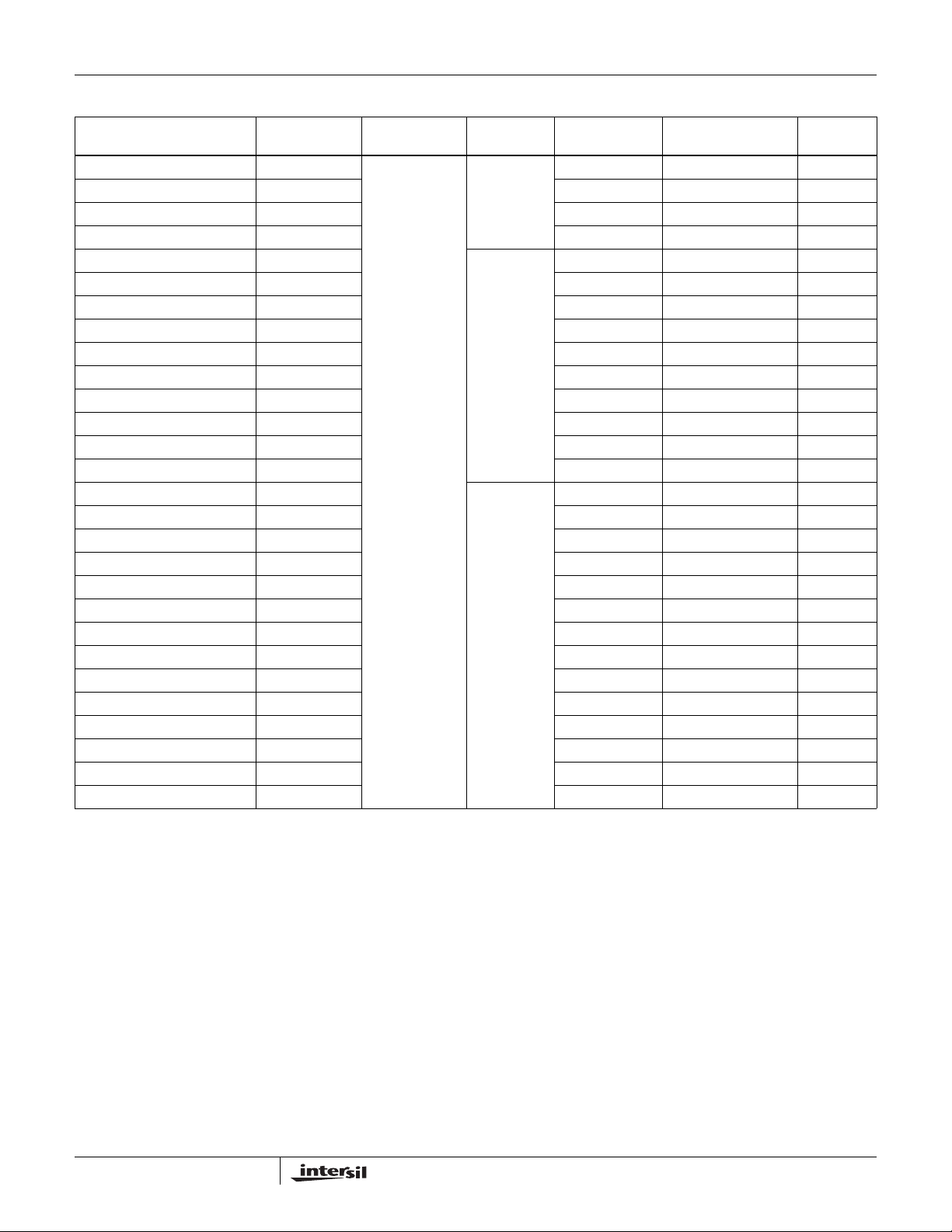
Block Diagram
www.BDTIC.com/Intersil
X9317
VCC (SUPPLY VOLTAGE)
UP/DOWN
(U/
INCREMENT
(
INC)
DEVICE SELECT
(
CS)
D)
VSS (GROUND)
CONTROL
AND
MEMORY
GENERAL
U/D
INC
CS
R
H
R
W
R
L
V
CC
V
SS
UP/DOWN
COUNTER
7-BIT
NONVOLATILE
MEMORY
STORE AND
RECALL
CONTROL
CIRCUITRY
ONE
OF
ONE
HUNDRED
DECODER
99
98
97
96
2
1
0
DETAILED
Pin Descriptions
PDIP/SOIC/MSOP TSSOP SYMBOL BRIEF DESCRIPTION
13INC
24U/DUp/Down. The U/D input controls the direction of the wiper movement.
35R
46V
SS
57R
68
R
71CS
82V
CC
Increment. Toggling INC while CS is low moves the wiper either up or down.
The high terminal is equivalent to one of the fixed terminals of a mechanical potentiometer.
H
Ground.
The wiper terminal is equivalent to the movable terminal of a mechanical potentiometer.
W
The low terminal is equivalent to one of the fixed terminals of a mechanical potentiometer.
L
Chip Select. The device is selected when the CS input is LOW, and de-selected when CS is
high.
Supply Voltage.
WIPER
SWITCHES
RESISTOR
ARRAY
R
H
R
L
R
W
5
FN8183.4
June 25, 2008

X9317
www.BDTIC.com/Intersil
Absolute Maximum Ratings Thermal Information
IW (10s) . . . . . . . . . . . . . . . . . . . . . . . . . . . . . . . . . . . . . . . . .±8.8mA
R
, RW, RL to Ground . . . . . . . . . . . . . . . . . . . . . . . . . . . . . . . . .+6V
H
Voltage on CS
with Respect to VSS. . . . . . . . . . . . . . . . . . . . . . . . . . . -1V to +7V
CAUTION: Do not operate at or near the maximum ratings listed for extended periods of time. Exposure to such conditions may adversely impact product reliability and
result in failures not covered by warranty.
, INC, U/D and V
CC
Junction Temperature Under Bias . . . . . . . . . . . . . .-65°C to +135°C
Storage Temperature. . . . . . . . . . . . . . . . . . . . . . . .-65°C to +150°C
Pb-free reflow profile . . . . . . . . . . . . . . . . . . . . . . . . . .see link below
http://www.intersil.com/pbfree/Pb-FreeReflow.asp
Potentiometer Specifications V
SYMBOL PARAMETER TEST CONDITIONS/NOTES
R
TOTAL
V
RH/RL
R
I
W
C
H/CL/CW
(Note 5)
V
CC
W
End-to-end Resistance Tolerance See “Ordering Information” beginning
RH/RL Terminal Voltage VSS = 0V V
Power Rating R
Wiper Resistance IW = 1mA, VCC = 5V 200 400 Ω
Wiper Current (Note 5) See “Test Circuit” on page 7 -4.4 +4.4 mA
(Note 7) Ref: 1kHz -120 dBV
Noise
Resolution 1%
Absolute Linearity (Note 1) V(R
Relative Linearity (Note 2) V(R
Temperature Coefficient (Note 5) V(RH) = VCC, V(RL) = 0V ±300 ppm/°C
R
TOTAL
Ratiometric Temperature Coefficient
(Notes 5, 6)
Potentiometer Capacitances See “Equivalent Circuit” on page 7 10/10/25 pF
Supply Voltage X9317 4.5 5.5 V
= Full Range, TA = Full Operating Temperature Range, unless otherwise stated.
CC
on page 2 for values
≥ 10kΩ 10 mW
TOTAL
R
= 1kΩ 25 mW
TOTAL
= 1mA, VCC = 2.7V 400 1000 Ω
I
W
) = VCC, V(RL) = 0V -1 +1 MI
H
) = VCC, V(RL) = 0V -0.2 +0.2 MI
H
) = VCC, V(RL) = 0V -20 +20 ppm/°C
V(R
H
X9317-2.7 2.7 5.5 V
MIN
(Note 8)
-20 +20 %
SS
TYP
(Note 4)
MAX
(Note 8) UNIT
V
CC
V
(Note 3)
(Note 3)
DC Electrical Specifications V
SYMBOL PARAMETER TEST CONDITIONS
I
CC1
I
CC2
I
SB
I
LI
V
IH
V
IL
C
(Note 5) CS, INC, U/D Input Capacitance V
IN
VCC Active Current (Increment) CS = VIL, U/D = VIL or VIH and
VCC Active Current (Store)
(non-volatile write)
Standby Supply Current CS ≥ VIH, U/D and INC =V
CS, INC, U/D Input Leakage Current VIN = V
CS, INC, U/D Input HIGH Voltage VCC x 0.7 VCC + 0.5 V
CS, INC, U/D Input LOW Voltage -0.5 VCC x 0.1 V
= 5V ±10%, TA = Full Operating Temperature Range, unless otherwise stated.
CC
=VIL/VIH @ min. t
INC
RL, RH, RW not connected
CS = VIH, U/D = VIL or VIH and INC = VIL
or V
. RL, RH, RW not connected
IH
RL, RH, RW not connected
to V
SS
= 5V, VIN = VSS, TA = +25°C,
CC
f=1MHz
CYC
IL
CC
6
MIN
(Note 8)
-10 +10 µA
TYP
(Note 4)
MAX
(Note 8) UNIT
50 µA
400 µA
1µA
10 pF
June 25, 2008
FN8183.4

X9317
www.BDTIC.com/Intersil
Endurance and Data Retention V
= 5V ±10%, TA = Full Operating Temperature Range.
CC
PARAMETER MIN UNIT
Minimum Endurance 100,000 Data changes per bit
Data Retention 100 Years
NOTES:
1. Absolute linearity is utilized to determine actual wiper voltage versus expected voltage = [V(R
V(R
W(n)(expected)
2. Relative linearity is a measure of the error in step size between taps = [V(R
3. 1 Ml = Minimum Increment = [V(R
4. Typical values are for T
) = n(V(RH)-V(RL))/99 + V(RL), with n from 0 to 99.
)-V(RL)]/99.
H
= +25°C and nominal supply voltage.
A
W(n+1)
)-(V(R
W(n)
W(n)(actual)
) - MI)]/MI.
)-V(R
W(n)(expected)
)]/MI
5. This parameter is not 100% tested.
6. Ratiometric temperature coefficient = (V(R
to 99.
7. Measured with wiper at tap position 99, R
-V(RW)
W)T1(n)
grounded, using test circuit.
L
T2(n)
)/[V(RW)
(T1-T2) x 106], with T1 and T2 being 2 temperatures, and n from 0
T1(n)
8. Parameters with MIN and/or MAX limits are 100% tested at +25°C, unless otherwise specified. T emperature limits established by characterization
and are not production tested.
Test Circuit Equivalent Circuit
R
TEST POINT
R
W
FORCE
CURRENT
R
H
10pF
TOTAL
C
H
R
W
C
W
25pF
C
10pF
R
L
L
AC Conditions of Test
Input pulse levels 0V to 3V
Input rise and fall times 10ns
Input reference levels 1.5V
AC Electrical Specifications V
= 5V ±10%, TA = Full Operating Temperature Range, unless otherwise stated.
CC
SYMBOL PARAMETER
t
Cl
(Note 5) INC HIGH to U/D Change 100 ns
t
lD
(Note 5) U/D to INC Setup 1 µs
t
DI
t
lL
t
lH
t
lC
t
CPHS
t
CPHNS
(Note 5)
t
IW
t
CYC
t
R, tF
(Note 5)
(Note 5) Power-up to Wiper Stable 5µs
t
PU
t
R VCC
(Note 5)
t
WR
CS to INC Setup 50 ns
INC LOW Period 960 ns
INC HIGH Period 960 ns
INC Inactive to CS Inactive 1 µs
CS Deselect Time (STORE) 10 ms
Deselect Time (NO STORE) 100 ns
CS
INC to RW Change 1 5 µs
INC Cycle Time 2 µs
Input Rise and Fall Time 500 µs
INC
VCC Power-up Rate 0.2 50 V/ms
Store Cycle 510ms
MIN
(Note 8)
TYP
(Note 4)
MAX
(Note 8) UNIT
7
FN8183.4
June 25, 2008

X9317
www.BDTIC.com/Intersil
Power-up and Down Requirements
The recommended power-up sequence is to apply VCC/VSS
first, then the potentiometer voltages. During power-up, the
data sheet parameters for the DCP do not fully apply until
AC Timing
CS
t
CYC
INC
U/D
R
t
CI
t
IW
W
t
IL
t
ID
t
IH
t
IC
t
DI
(3)
MI
Typical Performance Characteristic
0
-50
-100
-150
PPM
-200
-250
-300
-350
-45 -35 -25 -15 -5 5 15 25 35
-55
FIGURE 1. TYPICAL TOTAL RESISTANCE TEMPERATURE COEFFICIENT
1ms after V
always in effect. In order to prevent unwanted tap position
changes, or an inadvertent store, bring the CS
before or concurrently with the V
t
CPHS
45 55 65 75 85 95 105115 125
TEMPERATURE (°C)
reaches its final value. The VCC ramp spec is
CC
and INC high
pin on power-up.
CC
t
CPHNS
90% 90%
10%
t
F
t
R
8
FN8183.4
June 25, 2008

X9317
www.BDTIC.com/Intersil
Pin Descriptions
RH AND R
The high (RH) and low (RL) terminals of the X9317 are
equivalent to the fixed terminals of a mechanical
potentiometer. The terminology of R
relative position of the terminal in relation to wiper movement
direction selected by the U/D
potential on the terminal.
R
W
Rw is the wiper terminal and is equivalent to the movable
terminal of a mechanical potentiometer. The position of the
wiper within the array is determined by the control inputs.
The wiper terminal series resistance is typically 200Ω.
UP/DOWN (U/D
The U/D
and whether the counter is incremented or decremented.
INCREMENT (INC
The INC
move the wiper and either increment or decrement the
counter in the direction indicated by the logic level on the
U/D
CHIP SELECT (CS)
The device is selected when the CS
current counter value is stored in nonvolatile memory when
CS
is returned HIGH while the INC input is also HIGH. After
the store operation is complete, the X9317 will be placed in
the low power standby mode until the device is selected
once again.
L
and RH references the
L
input and not the voltage
)
input controls the direction of the wiper movement
)
input is negative-edge triggered. Toggling INC will
input.
input is LOW. The
Pin Configuration
DIP/SOIC/MSOP
INC
U/D
R
V
SS
1
2
X9317
3
H
4
V
8
CC
CS
7
R
L
6
R
W
5
Pin Names
SYMBOL DESCRIPTION
R
R
R
V
V
U/D
INC
CS
H
W
L
SS
CC
High terminal
Wiper terminal
Low terminal
Ground
Supply voltage
Up/Down control input
Increment control input
Chip select control input
Principles of Operation
There are three sections of the X9317: the control section,
the nonvolatile memory, and the resistor array. The control
section operates just like an up/down counter. The output of
this counter is decoded to turn on a single electronic switch
connecting a point on the resistor array to the wiper output.
The contents of the counter can be stored in nonvolatile
memory and retained for future use. The resistor array is
comprised of 99 individual resistors connected in series.
Electronic switches at either end of the array and between
each resistor provide an electrical connection to the wiper
pin, R
The wiper acts like its mechanical equivalent and does not
move beyond the first or last position. That is, the counter
does not wrap around when clocked to either extreme.
The electronic switches on the device operate in a “make
before break” mode when the wiper changes tap positions. If
the wiper is moved several positions, multiple taps are
connected to the wiper for t
R
a significant amount if the wiper is moved several positions.
When the device is powered-down, the last wiper position
stored will be maintained in the nonvolatile memory. When
power is restored, the contents of the memory are recalled
and the wiper is set to the value last stored.
.
W
(INC to VW change). The
value for the device can temporarily be reduced by
TOTAL
IW
Instructions and Programming
CS
V
INC
U/D
CC
1
2
3
4
TSSOP
X9317
9
R
8
L
R
7
W
V
SS
6
R
H
5
The INC, U/D and CS inputs control the movement of the
wiper along the resistor array. With CS
is selected and enabled to respond to the U/D
inputs. HIGH to LOW transitions on INC
decrement (depending on the state of the U/D
counter. The output of this counter is decoded to select one
of one hundred wiper positions along the resistive array.
The value of the counter is stored in nonvolatile memory
whenever CS
HIGH.
set LOW, the device
and INC
will increment or
input) a 7-bit
transitions HIGH while the INC input is also
FN8183.4
June 25, 2008

X9317
www.BDTIC.com/Intersil
The system may select the X9317, move the wiper and
deselect the device without having to store the latest wiper
position in nonvolatile memory. After the wiper movement is
performed as previously described and once the new
position is reached, the system must keep INC
taking CS
until changed by the system or until a power-up/down cycle
recalls the previously stored data.
This procedure allows the system to always power-up to a
preset value stored in nonvolatile memory; then during
system operation minor adjustments could be made. The
adjustments might be based on user preference, system
parameter changes due to temperature drift, etc.
The state of U/D
This allows the host system to enable the device and then
move the wiper up and down until the proper trim is attained.
HIGH. The new wiper position will be maintained
may be changed while CS remains LOW.
LOW while
Mode Selection
CS INC U/D MODE
L H Wiper up
L L Wiper down
H X Store wiper position to nonvolatile
memory
H X X Standby
L X No store, return to standby
L H Wiper Up (not recommended)
L L Wiper Down (not recommended)
Applications Information
Electronic digitally controlled (XDCP) potentiometers provide
three powerful application advantages:
1. the variability and reliability of a solid-state potentiometer,
2. the flexibility of computer-based di gital controls, and
3. the retentivity of nonvolatile memory used for the storage
of multiple potentiometer settings or data.
10
FN8183.4
June 25, 2008

Basic Configurations of Electronic Potentiometers
www.BDTIC.com/Intersil
V
REF
R
H
R
W
R
L
X9317
V
REF
I
Basic Circuits
R
+V
IN
1
V
REF
VOLTAGE REGULATOR
THREE TERMINAL POTENTIOMETER;
VARIABLE VOLTAGE DIVIDER
+5V
I
adj
317
R
W
V
R
2
OUT
R
+
-
= VW/R
1
LMC7101
TWO TERMINAL VARIABLE RESISTOR;
VARIABLE CURRENT
CASCADING TECHNIQUESBUFFERED REFERENCE VOLTAGE
+V +V
V
OUT
+V
W
R
W
(a) (b)
X
OFFSET VOLTAGE ADJUSTMENT
R
VO (REG)V
V
S
10kΩ
1
100kΩ
R
2
+5V
-
+
LMC7101
SINGLE SUPPLY INVERTING AMPLIFIER
R
R
1
2
V
S
100k
+5V
R
W
100k
VO = (R2/R1)V
COMPARATOR WITH HYSTERESIS
LT311A
V
S
V
O
}
R
-
+
}
R
2
1
+5V
-
+
LMC7101
S
V
O
V
O
10kΩ10kΩ
VO (REG) = 1.25V (1+R2/R1)+I
adj R2
+5V
11
= {R1/(R1+R2)} VO(max)
V
UL
V
= {R1/(R1+R2)} VO(min)
LL
FN8183.4
June 25, 2008

X9317
www.BDTIC.com/Intersil
Mini Small Outline Plastic Packages (MSOP)
N
EE1
INDEX
AREA
AA1A2
TOP VIEW
-H-
SIDE VIEW
12
b
e
D
NOTES:
1. These package dimensions are within allowable dimensions of
JEDEC MO-187BA.
2. Dimensioning and tolerancing per ANSI Y14.5M-1994.
3. Dimension “D” does not include mold flash, protrusions or gate
burrs and are measured at Datum Plane. Mold flash, protrusion
and gate burrs shall not exceed 0.15mm (0.006 inch) per side.
4. Dimension “E1” does not include interlead flash or protrusions
and are measured at Datum Plane. Interlead flash and
protrusions shall not exceed 0.15mm (0.006 inch) per side.
5. Formed leads shall be planar with respect to one another within
0.10mm (0.004) at seating Plane.
6. “L” is the length of terminal for soldering to a substrate.
7. “N” is the number of terminal positions.
8. Terminal numbers are shown for reference only.
9. Dimension “b” does not include dambar protrusion. Allowable
dambar protrusion shall be 0.08mm (0.003 inch) total in excess
of “b” dimension at maximum material condition. Minimum space
between protrusion and adjacent lead is 0.07mm (0.0027 inch).
- H -
-A -
.
10. Datums and to be determined at Datum plane
11. Controlling dimension: MILLIMETER. Converted inch dimensions are for reference only.
-B-
0.20 (0.008) A
GAUGE
PLANE
SEATING
PLANE
0.10 (0.004) C
-A-
0.20 (0.008) C
- B -
0.25
(0.010)
-C-
SEATING
PLANE
a
0.20 (0.008) C
- H -
B
4X θ
C
D
4X θ
L1
C
C
L
E
1
END VIEW
R1
R
L
-B-
M8.118 (JEDEC MO-187AA)
8 LEAD MINI SMALL OUTLINE PLASTIC PACKAGE
INCHES MILLIMETERS
SYMBOL
A 0.037 0.043 0.94 1.10 -
A1 0.002 0.006 0.05 0.15 -
A2 0.030 0.037 0.75 0.95 -
b 0.010 0.014 0.25 0.36 9
c 0.004 0.008 0.09 0.20 -
D 0.116 0.120 2.95 3.05 3
E1 0.116 0.120 2.95 3.05 4
e 0.026 BSC 0.65 BSC -
E 0.187 0.199 4.75 5.05 -
L 0.016 0.028 0.40 0.70 6
L1 0.037 REF 0.95 REF -
N8 87
R 0.003 - 0.07 - -
R1 0.003 - 0.07 - -
05
α
o
o
0
15
o
o
6
o
5
o
0
15
o
o
6
Rev. 2 01/03
NOTESMIN MAX MIN MAX
-
-
12
FN8183.4
June 25, 2008

X9317
www.BDTIC.com/Intersil
Thin Shrink Small Outline Plastic Packages (TSSOP)
N
INDEX
AREA
123
0.05(0.002)
-AD
e
b
0.10(0.004) C AM BS
NOTES:
1. These package dimensions are within allowable dimensions of
JEDEC MO-153-AC, Issue E.
2. Dimensioning and tolerancing per ANSI Y14.5M-1982.
3. Dimension “D” does not include mold flash, protrusions or gate burrs.
Mold flash, protrusion and gate burrs shall not exceed 0.15mm
(0.006 inch) per side.
4. Dimension “E1” does not include interlead flash or protrusions. Interlead flash and protrusions shall not exceed 0.15mm (0.006 inch) per
side.
5. The chamfer on the body is optional. If it is not present, a visual index
feature must be located within the crosshatched area.
6. “L” is the length of terminal for soldering to a substrate.
7. “N” is the number of terminal positions.
8. Terminal numbers are shown for reference only.
9. Dimension “b” does not include dambar protrusion. Allowable dambar
protrusion shall be 0.08mm (0.003 inch) total in excess of “b” dimension at maximum material condition. Minimum space between protrusion and adjacent lead is 0.07mm (0.0027 inch).
10. Controlling dimension: MILLIMETER. Converted inch dimensions
are not necessarily exact. (Angles in degrees)
E1
-B-
SEATING PLANE
A
-C-
M
0.25(0.010) BM M
E
α
A1
0.10(0.004)
GAUGE
PLANE
0.25
0.010
A2
L
c
M8.173
8 LEAD THIN SHRINK NARROW BODY SMALL OUTLINE
PLASTIC PACKAGE
INCHES MILLIMETERS
SYMBOL
A - 0.047 - 1.20 -
A1 0.002 0.006 0.05 0.15 -
A2 0.031 0.051 0.80 1.05 -
b 0.0075 0.0118 0.19 0.30 9
c 0.0035 0.0079 0.09 0.20 -
D 0.116 0.120 2.95 3.05 3
E1 0.169 0.177 4.30 4.50 4
e 0.026 BSC 0.65 BSC -
E 0.246 0.256 6.25 6.50 -
L 0.0177 0.0295 0.45 0.75 6
N8 87
o
α
0
o
8
o
0
o
8
Rev. 1 12/00
NOTESMIN MAX MIN MAX
-
13
FN8183.4
June 25, 2008
Small Outline Package Family (SO)
www.BDTIC.com/Intersil
A
D
NN
(N/2)+1
X9317
h X 45°
PIN #1
E
C
SEATING
PLANE
0.004 C
E1
B
0.010 BM CA
I.D. MARK
1
e
0.010 BM CA
(N/2)
c
SEE DETAIL “X”
L1
H
A2
GAUGE
PLANE
A1
b
DETAIL X
L
4° ±4°
MDP0027
SMALL OUTLINE PACKAGE FAMILY (SO)
INCHES
SO16
SYMBOL
A 0.068 0.068 0.068 0.104 0.104 0.104 0.104 MAX -
A1 0.006 0.006 0.006 0.007 0.007 0.007 0.007 ±0.003 -
A2 0.057 0.057 0.057 0.092 0.092 0.092 0.092 ±0.002 -
b 0.017 0.017 0.017 0.017 0.017 0.017 0.017 ±0.003 -
c 0.009 0.009 0.009 0.011 0.011 0.011 0.011 ±0.001 -
D 0.193 0.341 0.390 0.406 0.504 0.606 0.704 ±0.004 1, 3
E 0.236 0.236 0.236 0.406 0.406 0.406 0.406 ±0.008 -
E1 0.154 0.154 0.154 0.295 0.295 0.295 0.295 ±0.004 2, 3
e 0.050 0.050 0.050 0.050 0.050 0.050 0.050 Basic -
L 0.025 0.025 0.025 0.030 0.030 0.030 0.030 ±0.009 -
L1 0.041 0.041 0.041 0.056 0.056 0.056 0.056 Basic -
h 0.013 0.013 0.013 0.020 0.020 0.020 0.020 Reference -
N 8 14 16 16 20 24 28 Reference -
NOTES:
1. Plastic or metal protrusions of 0.006” maximum per side are not included.
2. Plastic interlead protrusions of 0.010” maximum per side are not included.
3. Dimensions “D” and “E1” are measured at Datum Plane “H”.
4. Dimensioning and tolerancing per ASME Y14.5M-1994
(0.150”)
SO16 (0.300”)
(SOL-16)
SO20
(SOL-20)
SO24
(SOL-24)
SO28
(SOL-28)
TOLERANCE NOTESSO-8 SO-14
A
0.010
Rev. M 2/07
14
FN8183.4
June 25, 2008

Plastic Dual-In-Line Packages (PDIP)
www.BDTIC.com/Intersil
X9317
SEATING
PLANE
D
A2
A
L
L
e
b
A1
NOTE 5
c
E
eA
eB
N
PIN #1
E1
INDEX
12 N/2
MDP0031
PLASTIC DUAL-IN-LINE PACKAGE
INCHES
SYMBOL
A 0.210 0.210 0.210 0.210 0.210 MAX
A1 0.015 0.015 0.015 0.015 0.015 MIN
A2 0.130 0.130 0.130 0.130 0.130 ±0.005
b 0.018 0.018 0.018 0.018 0.018 ±0.002
b2 0.060 0.060 0.060 0.060 0.060 +0.010/-0.015
c 0.010 0.010 0.010 0.010 0.010 +0.004/-0.002
D 0.375 0.750 0.750 0.890 1.020 ±0.010 1
E 0.310 0.310 0.310 0.310 0.310 +0.015/-0.010
E1 0.250 0.250 0.250 0.250 0.250 ±0.005 2
e 0.100 0.100 0.100 0.100 0.100 Basic
eA 0.300 0.300 0.300 0.300 0.300 Basic
eB 0.345 0.345 0.345 0.345 0.345 ±0.025
L 0.125 0.125 0.125 0.125 0.125 ±0.010
N 8 14 16 18 20 Reference
NOTES:
1. Plastic or metal protrusions of 0.010” maximum per side are not included.
2. Plastic interlead protrusions of 0.010” maximum per side are not included.
3. Dimensions E and eA are measured with the leads constrained perpendicular to the seating plane.
4. Dimension eB is measured with the lead tips unconstrained.
5. 8 and 16 lead packages have half end-leads as shown.
TOLERANCE NOTESPDIP8 PDIP14 PDIP16 PDIP18 PDIP20
b2
Rev. C 2/07
All Intersil U.S. products are manufactured, assembled and tested utilizing ISO9000 quality systems.
Intersil Corporation’s quality certifications can be viewed at www.intersil.com/design/quality
Intersil products are sold by description only. Intersil Corporation reserves the right to make changes in circuit design, software and/or specifications at any time without
notice. Accordingly, the reader is cautioned to verify that data sheets are current before placing orders. Information furnished by Intersil is believed to be accurate and
reliable. However, no responsibility is assumed by Intersil or its subsidiaries for its use; nor for any infringements of patents or other rights of third parties which may result
from its use. No license is granted by implic atio n or other wise u nde r any p a tent or patent rights of Intersil or its subsidi aries.
For information regarding Intersil Corporation and its products, see www.intersil.com
15
FN8183.4
June 25, 2008
 Loading...