®
www.BDTIC.com/Intersil
X93156
Single Digitally Controlled Potentiometer (XDCP™)
Data Sheet November 21, 2007
Low Noise, Low Power, 3 wire Up/Down,
32 Taps
The Intersil X93156 is a three-terminal digitally controlled
potentiometer (XDCP). The device consists of a resistor
array, wiper switches, a control section, and nonvolatile
memory. The wiper position is controlled by an Up/Down
interface.
The potentiometer is implemented by a resistor array
composed of 31 resistive elements and a wiper switching
network. The position of the wiper element is controlled by
the CS
, U/D, and INC inputs. The position of the wiper can
be stored in a nonvolatile memory and then be recalled upon
a subsequent power-up operation.
The device can be used as a three-terminal potentiometer or
as a two terminal variable resistor in a wide variety of
applications including the programming of bias voltages,
LCD brightness and contrast control as well as the
implementation of ladder networks.
Features
• Solid-state potentiometer
• Up/Down interface
• 32 wiper tap points
- Wiper position stored in nonvolatile memory and
recalled on power-up
• 31 resistive elements
- Temperature compensated
- Maximum resistance tolerance of ±25%
- Terminal voltage, 0 to V
• Low power CMOS
-V
= 2.7V to 5.5V
CC
- Active current, 200µA typ.
- Standby current, 2µA max.
• High reliability
- Endurance 200,000 data changes per bit
- Register data retention, 100 years
CC
FN8182.3
•R
value = 12.5kΩ, 50kΩ
TOTAL
• Package
- 8 Ld MSOP
- Pb-free Available (RoHS compliant)
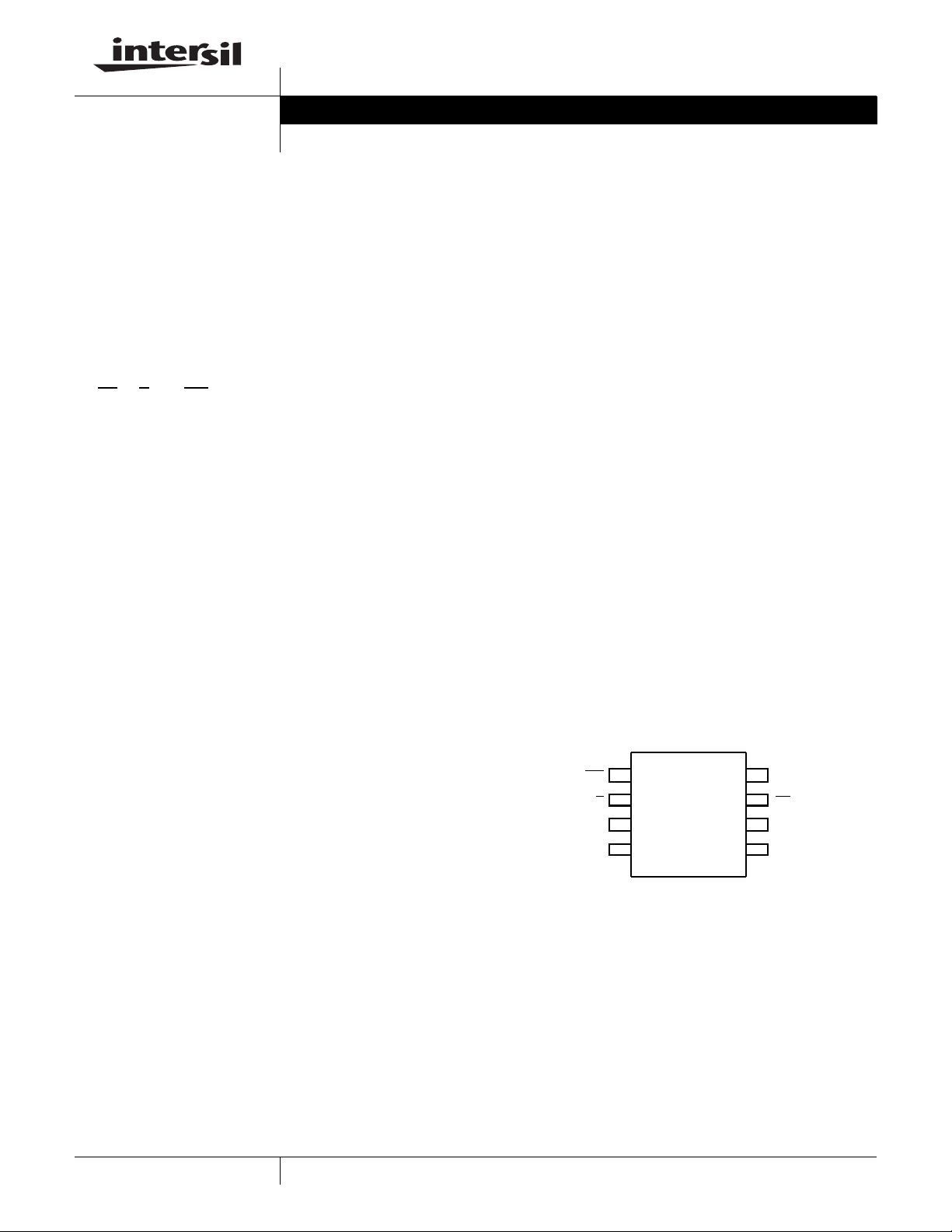
Pinout
X93156
(8 LD MSOP)
TOP VIEW
INC
U/D
V
1
2
R
H
SS
X93156
3
4
8
V
CC
7
CS
R
6
5
L
Rw
1
CAUTION: These devices are sensitive to electrostatic discharge; follow proper IC Handling Procedures.
1-888-INTERSIL or 1-888-468-3774
XDCP is a trademark of Intersil Americas Inc. Copyright Intersil Americas Inc. 2005, 2007. All Rights Reserved
| Intersil (and design) is a registered trademark of Intersil Americas Inc.
All other trademarks mentioned are the property of their respective owners.

X93156
www.BDTIC.com/Intersil
Ordering Information
PART
PART NUMBER
MARKING
X93156WM8I AGO 5 ±10% 12.5 -40 to +85 8 Ld MSOP M8.118
X93156WM8I-2.7* AGR 2.7 to 5.5 12.5 -40 to +85 8 Ld MSOP M8.118
X93156UM8I-2.7* AGP 2.7 to 5.5 50 -40 to +85 8 Ld MSOP M8.118
X93156WM8IZ-2.7* (Note) DCK 2.7 to 5.5 12.5 -40 to +85 8 Ld MSOP (Pb-free) M8.118
X93156UM8IZ-2.7* (Note) AKV 2.7 to 5.5 50 -40 to +85 8 Ld MSOP (Pb-free) M8.118
X93156WM8IZ DCJ 5 ±10% 12.5 -40 to +85 8 Ld MSOP (Pb-free) M8.118
*Add “-T1” suffix for tape and reel. Please refer to TB347 for details on reel specifications.
NOTE: These Intersil Pb-free plastic packaged products employ special Pb-free material sets; molding compounds/die attach materials and 100%
matte tin plate PLUS ANNEAL - e3 termination finish, which is RoHS compliant and compatible with both SnPb and Pb-free soldering operations.
Intersil Pb-free products are MSL classified at Pb-free peak reflow temperatures that meet or exceed the Pb-free requirements of IPC/JEDEC J
STD-020.
V
CC
RANGE (V)
R
TOTAL
(kΩ)
TEMP
RANGE (°C) PACKAGE
PKG.
DWG. #
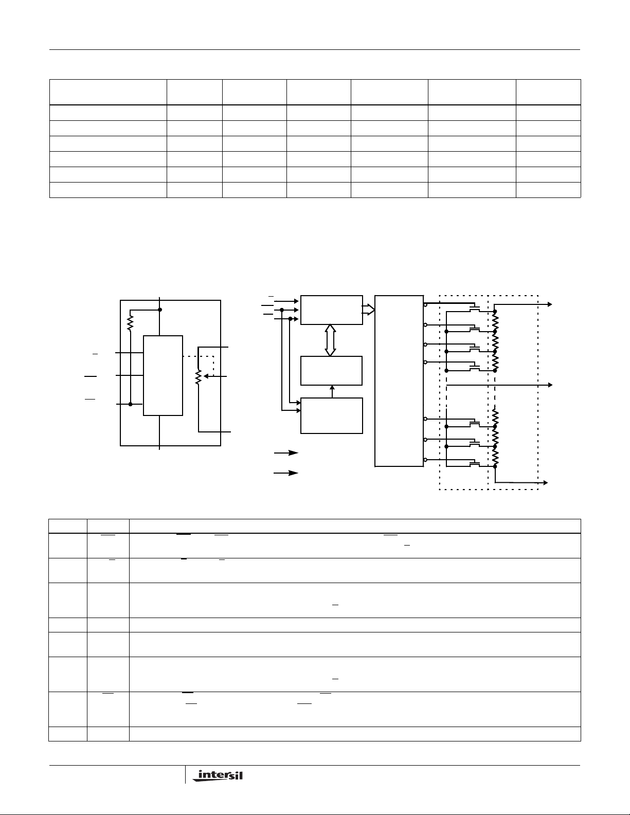
Block Diagram
(SUPPLY VOLTAGE)
V
CC
30k
U/D
INC
CS
5-BIT
UP/DOWN
COUNTER
31
30
R
H
R
UP/DOWN
)
(U/D
INCREMENT
)
(INC
DEVICE SELECT
(CS
)
CONTROL
AND
MEMORY
(GROUND)
V
SS
GENERAL
H
5-BIT
R
W
R
L
V
CC
V
SS
NONVOLATILE
MEMORY
STORE AND
CONTROL
RECALL
CIRCUITRY
Pin Descriptions
MSOP SYMBOL BRIEF DESCRIPTION
1INC
2U/D
3R
4V
5RwR
6R
7CS
8V
Increment (INC). The INC input is negative-edge triggered. Toggling INC will move the wiper and either increment or
decrement the counter in the direction indicated by the logic level on the U/D
Up/Down (U/D). The U/D input controls the direction of the wiper movement and whether the counter is incremented or
decremented.
RH. The R
H
voltage is VSS and the maximum is VCC. The terminology of RH and RL references the relative position of the terminal in
relation to wiper movement direction selected by the U/D
Ground.
SS
. The Rw pin of the X93156 is the wiper terminal of the potentiometer which is equivalent to the movable terminal of a
W
mechanical potentiometer.
RL. The R
L
voltage is VSS and the maximum is VCC. The terminology of RH and RL references the relative position of the terminal in
relation to wiper movement direction selected by the U/D
and RL pins of the X93156 are equivalent to the fixed terminals of a mechanical potentiometer. The minimum
H
input.
and RL pins of the X93156 are equivalent to the fixed terminals of a mechanical potentiometer. The minimum
H
input.
Chip Select (CS). The device is selected when the CS input is LOW. The current counter value is stored in nonvolatile
memory when CS
is returned HIGH while the INC input is also HIGH. After the store operation is complete, the X93156 will
be placed in the low power standby mode until the device is selected once again.
Supply Voltage.
CC
ONE
OF
THIRTY
TWO
DECODER
29
28
2
1
0
DETAILED
input.
TRANSFER
GATES
RESISTOR
ARRAY
R
W
R
L
2
FN8182.3
November 21, 2007

X93156
www.BDTIC.com/Intersil
Absolute Maximum Ratings Thermal Information
Temperature under bias. . . . . . . . . . . . . . . . . . . . . .-65°C to +135°C
Storage temperature . . . . . . . . . . . . . . . . . . . . . . . .-65°C to +150°C
Voltage on CS
, INC, U/D, RH, RL and V
CC
with respect to VSS. . . . . . . . . . . . . . . . . . . . . . . . . . .-1V to +6.5V
Maximum resistor current . . . . . . . . . . . . . . . . . . . . . . . . . . . . . 2mA
CAUTION: Do not operate at or near the maximum ratings listed for extended periods of time. Exposure to such conditions may adversely impact product reliability and
result in failures not covered by warranty.
NOTE:
is measured with the component mounted on a high effective thermal conductivity test board in free air. See Tech Brief TB379 for details.
1. θ
JA
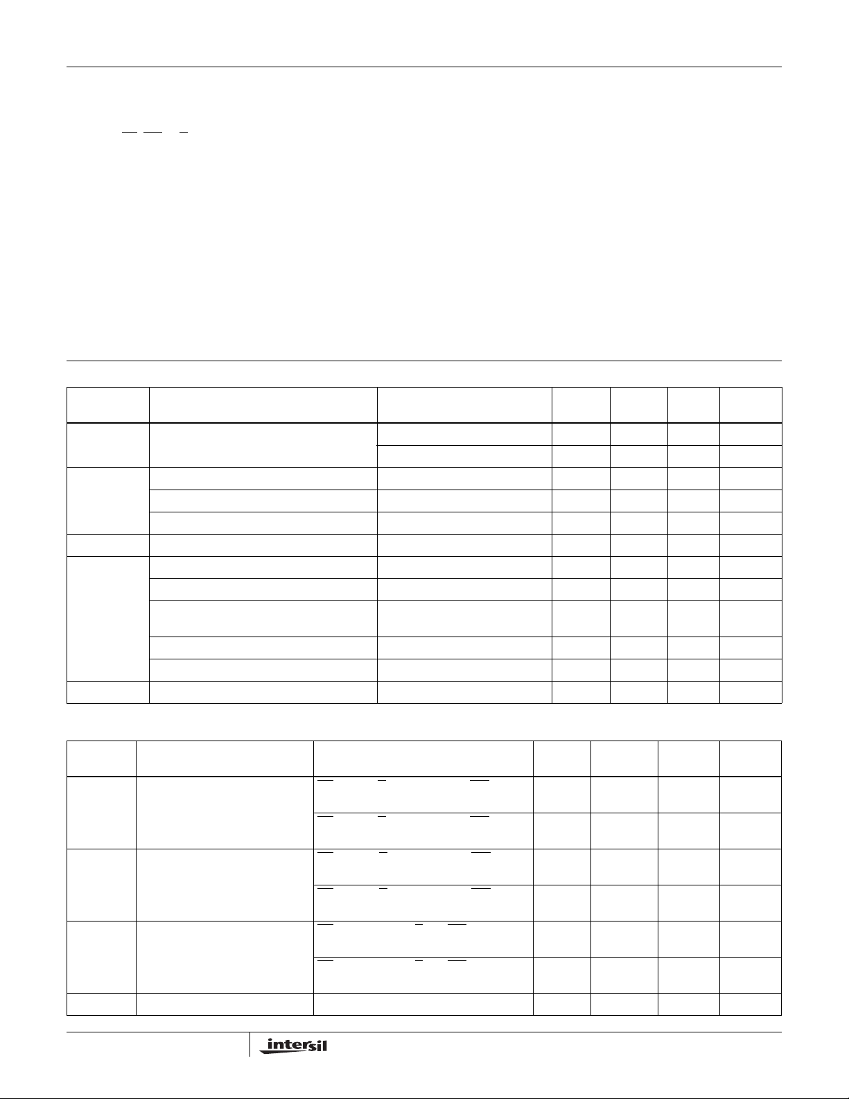
Potentiometer Specifications Over recommended operating conditions unless otherwise stated.
SYMBOL PARAMETER TEST CONDITIONS/NOTES
R
TOT
V
R
I
W
C
H/CL/CW
R
W
End to end resistance 9.375 12.5 15.625 kΩ
RH, RL terminal voltages 0 V
Power rating (Note 7) 1 mW
Noise Ref: 1kHz (Note 7) -120 dBV
Wiper Resistance 1100 Ω
Wiper Current (Note 6) ±0.6 mA
Resolution 3%
Absolute linearity (Note 2) V
H(n)(actual)
(Note 4)
Relative linearity (Note 3) V
temperature coefficient (Note 7) ±35 ppm/°C
R
TOTAL
H(n + 1)
Potentiometer capacitances See circuit #2 (Note 7) 10/10/25 pF
Thermal Resistance (Typical, Note 1) θ
8 Ld MSOP. . . . . . . . . . . . . . . . . . . . . . . . . . . . . . . . 190
Pb-free reflow profile . . . . . . . . . . . . . . . . . . . . . . . . . .see link below
http://www.intersil.com/pbfree/Pb-FreeReflow.asp
Recommended Operating Conditions
Temperature Range
Industrial. . . . . . . . . . . . . . . . . . . . . . . . . . . . . . . . .-40°C to +85°C
Supply Voltage V
X93156xxx-2.7. . . . . . . . . . . . . . . . . . . . . . . 2.7V to 5.5V (Note 8)
X93156xxx . . . . . . . . . . . . . . . . . . . . . . . . . . . . . . . . . . . .5V ±10%
- V
H(n)(expected)
- [V
] (Note 4) ±0.5 MI
H(n) + MI
CC
MIN
(Note 9) TYP
37.5 50 62.5 kΩ
MAX
(Note 9) UNIT
CC
±1 MI
(°C/W)
JA
V
DC Electrical Specifications Over recommended operating conditions unless otherwise specified.
SYMBOL PARAMETER TEST CONDITIONS
I
CC1
I
CC2
I
SB
I
VCC active current (Increment) CS = VIL, U/D = VIL or VIH and INC = 0.4V
VCC active current (Store)
(EEPROM Store)
@ max. t
CS
@ max. t
CYC VCC
= VIL, U/D = VIL or VIH and INC = 0.4V
CYC VCC
CS = VIH, U/D = VIL or VIH and INC =
@max. t
V
IH
CS
= VIH, U/D = VIL or VIH and INC =
V
@max. t
IH
= 3V
= 5V
WR VCC
WR VCC
= 3V
= 5V
Standby supply current CS = VCC - 0.3V, U/D and INC = VSS or
CS input leakage current VIN = V
LI
- 0.3V V
V
CC
= VCC - 0.3V, U/D and INC = VSS or
CS
- 0.3V V
V
CC
CC
CC
CC
= 3V
= 5V
3
MIN
(Note 9)
TYP
(Note 5)
MAX
(Note 9) UNIT
50 250 µA
200 300 µA
600 µA
1400 µA
1µA
2µA
±1 µA
November 21, 2007
FN8182.3
 Loading...