intersil X93154 DATA SHEET

®
www.BDTIC.com/Intersil
X93154
Low Noise, Low Power, 32 Taps
Data Sheet February 19, 2008
Digitally Controlled Potentiometer
(XDCP™)
The Intersil X93154 is a digitally controlled potentiometer
(XDCP). The device consists of a resistor array, wiper
switches, a control section, and nonvolatile memory. The
wiper position is controlled by a 3-wire interface.
The potentiometer is implemented by a resistor array
composed of 31 resistive elements and a wiper switching
network. The position of the wiper element is controlled by
the CS
, U/D, and INC inputs. The position of the wiper can
be stored in nonvolatile memory and then be recalled upon
during a subsequent power-up operation.
The device is connected as a two-terminal variable resistor
and can be used in a wide variety of applications including:
- Bias and Gain Control
- LCD Contrast Adjustment
FN8180.3
Features
• Solid-State Potentiometer
• 3-Wire Serial Interface
• 32 Wiper Tap Points
- Wiper Position Stored in Nonvolatile Memory and
Recalled on Power-up
• 31 Resistive Elements
- Temperature Compensated
- Maximum Resistance Tolerance of ±30%
- Terminal V oltage, 0 to V
• Low Power CMOS
-V
= 3V±10%
CC
- Active Current, 250µA max.
- Standby Current, 1µA max.
• High Reliability
- Endurance 200,000 Data Changes Per Bit
- Register Data Retention, 100 years
CC
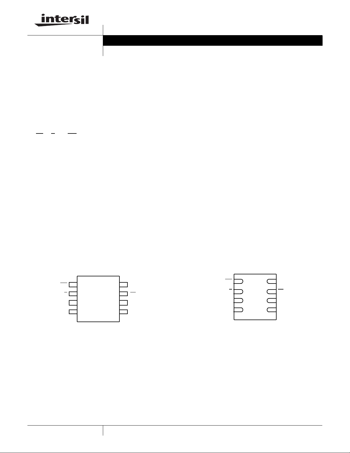
Pinouts
INC
U/D
V
TOTAL
Value = 50kΩ
•R
• Packages
- 8 Ld MSOP, TDFN
• Pb-free Available (RoHS Compliant)
X93154
(8 LD MSOP)
TOP VIEW
8
1
2
R
H
3
SS
4
V
CC
7
CS
R
6
5
NC
L
*
*
NC can be left unconnected, or connected to any voltage between VSS
and V
CC
INC
U/D
V
R
SS
1
2
3
H
4
X93154
(8 LD TDFN)
TOP VIEW
8
V
CC
7
CS
6
R
L
*
5
NC
1
XDCP is a trademark of Intersil Americas Inc. Copyright Intersil Americas Inc. 2004, 2005, 2008. All Rights Reserved
CAUTION: These devices are sensitive to electrostatic discharge; follow proper IC Handling Procedures.
1-888-INTERSIL or 1-888-468-3774
| Intersil (and design) is a registered trademark of Intersil Americas Inc.
All other trademarks mentioned are the property of their respective owners.

X93154
www.BDTIC.com/Intersil
Ordering Information
PKG.
PART NUMBER PART MARKING VCC LIMITS (V) R
(kΩ) TEMP RANGE (°C) PACKAGE
TOTAL
DWG. #
X93154UM8I-3* AGK 3 ±10% 50 -40 to +85 8 Ld MSOP M8.118
X93154UM8IZ-3* (Note) AIW -40 to +85 8 Ld MSOP (Pb-free) M8.118
X93154UU8IZ-3* (Note) AKH -40 to +85 8 Ld TDFN (Pb-free) L8.2.5x2
*Add "T1" suffix for tape and reel. Please refer to TB347 for details on reel specifications.
NOTE: These Intersil Pb-free plastic packaged products employ special Pb-free material sets; molding compounds/die attach materials and 100%
matte tin plate PLUS ANNEAL - e3 termination finish, which is RoHS compliant and compatible with both SnPb and Pb-free soldering operations.
Intersil Pb-free products are MSL classified at Pb-free peak reflow temperatures that meet or exceed the Pb-free requirements of IPC/JEDEC J
STD-020.
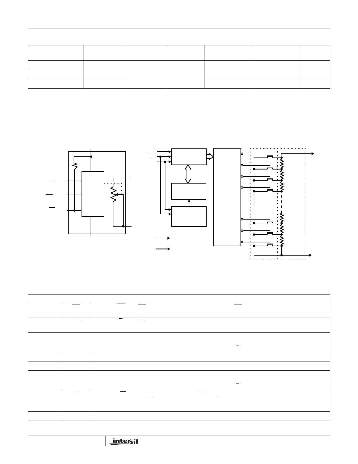
Block Diagram
V
(SUPPLY VOLTAGE)
CC
30k
U/D
INC
CS
5-BIT
UP/DOWN
COUNTER
31
30
R
H
R
UP/DOWN
)
(U/D
INCREMENT
(INC
)
DEVICE SELECT
(CS
)
CONTROL
AND
MEMORY
V
(Ground)
SS
H
5-BIT
NONVOLATILE
MEMORY
STORE AND
CONTROL
RECALL
R
L
V
CC
V
SS
CIRCUITRY
ONE
THIRTY
TWO
DECODER
GENERAL
Pin Descriptions
MSOP, TDFN SYMBOL BRIEF DESCRIPTION
1INC
2U/D
3R
4V
5NCNo Connection (or can be connected to any voltage between V
6R
7CS
8V
Increment (INC). The INC input is negative-edge triggered. Toggling INC will move the wiper and either increment
or decrement the counter in the direction indicated by the logic level on the U/D
Up/Down (U/D). The U/D input controls the direction of the wiper movement and whether the counter is incremented
or decremented.
RH. The R
H
minimum voltage is V
and RL pins of the X93154 are equivalent to the fixed terminals of a mechanical potentiometer. The
H
and the maximum is VCC. The terminology of RH and RL references the relative position of
SS
the terminal in relation to wiper movement direction selected by the U/D
Ground.
SS
RL. The R
L
minimum voltage is V
the terminal in relation to wiper movement direction selected by the U/D
and RL pins of the X93154 are equivalent to the fixed terminals of a mechanical potentiometer. The
H
and the maximum is VCC. The terminology of RH and RL references the relative position of
SS
Chip Select (CS). The device is selected when the CS input is LOW. The current counter value is stored in
nonvolatile memory when CS
is returned HIGH while the INC input is also HIGH. After the store operation is
complete, the X93154 will be placed in the low power standby mode until the device is selected once again.
Supply Voltage.
CC
29
28
OF
and VCC.)
SS
2
1
0
DETAILED
input.
input.
TRANSFER
GATES
input.
RESISTOR
ARRAY
R
L
2
FN8180.3
February 19, 2008

X93154
www.BDTIC.com/Intersil
Absolute Maximum Ratings Thermal Information
Voltage on CS, INC, U/D, RH, RL and V
with respect to VSS . . . . . . . . . . . . . . . . . . . . . . . . . .-1V to +6.5V
Maximum Resistor Current . . . . . . . . . . . . . . . . . . . . . . . . . . . . 2mA
CC
Recommended Operating Conditions
Temperature Range
Industrial. . . . . . . . . . . . . . . . . . . . . . . . . . . . . . . . .-40°C to +85°C
Supply Voltage
. . . . . . . . . . . . . . . . . . . . . . . . . . . . . . . . . .3V ±10% (Note 6)
V
CC
CAUTION: Do not operate at or near the maximum ratings listed for extended periods of time. Exposure to such conditions may adversely impact product reliability and
result in failures not covered by warranty.
NOTES:
1. Absolute linearity is utilized to determine actual wiper voltage versus expected voltage = (V
n = 1.. 29 only
2. Relative linearity is a measure of the error in step size between taps = V
3. 1 Ml = Minimum Increment = R
4. Typical values are for T
5. Limits established by characterization and are not production tested.
6. When performing multiple write operations, V
7. Parts are 100% tested at +25°C. Over-temperature limits established by characterization and are not production tested.
= +25°C and nominal supply voltage.
A
TOT
/31.
must not decrease by more than 150mV from its initial value.
CC
Storage Temperature. . . . . . . . . . . . . . . . . . . . . . . .-65°C to +150°C
Temperature Under Bias . . . . . . . . . . . . . . . . . . . . .-65°C to +135°C
Pb-free Reflow Profile . . . . . . . . . . . . . . . . . . . . . . . . .see link below
http://www.intersil.com/pbfree/Pb-FreeReflow.asp
H(n+1)
(actual)-V
H(n)
-[V
+ Ml] = ±0.5 Ml, n = 1 .. 29 only.
H(n)
(expected)) = ±1 Ml Maximum.
H(n)
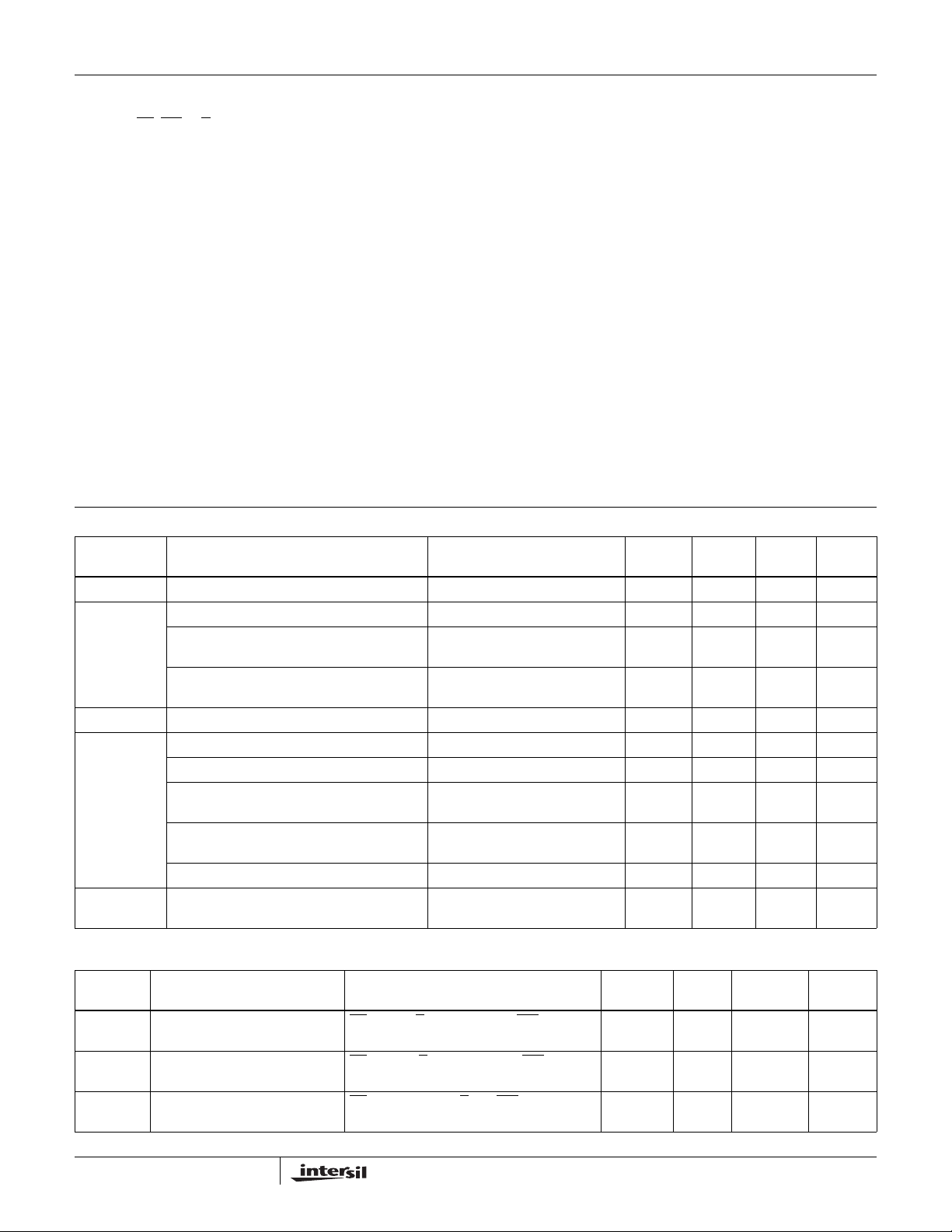
Potentiometer Specifications Over recommended operating conditions unless otherwise stated.
MIN
SYMBOL PARAMETER TEST CONDITIONS/NOTES
R
TOT
V
R
W
I
W
C
H/CL/CW
R
End-to-End Resistance 35 50 65 kΩ
RH, RL Terminal Voltages 0 V
Power Rating R
Noise Ref: 1kHz -120 dBV
Wiper Resistance (Note 5) 1000 Ω
Wiper Current (Note 5) 0.6 mA
Resolution 3%
Absolute Linearity
Relative Linearity (Note 2) V
Temperature Coefficient (Note 5) ±35 ppm/°C
R
TOTAL
Potentiometer Capacitances See “Circuit #2 SPICE Macro
(Note 1) V
= 50kΩ 1mW
TOTAL
H(n)(actual)-VH(n)(expected)
-[V
H(n+1)
Model” on page 4
]±0.5MI
H(n)+MI
(Note 7)
DC Electrical Specifications Over recommended operating conditions, unless otherwise specified.
MIN
SYMBOL PARAMETER TEST CONDITIONS
I
CC1
I
CC2
I
SB
VCC Active Current (Increment) CS = VIL, U/D = VIL or VIH and INC =0.4V @
VCC Active Current (Store)
(EEPROM Store)
Standby Supply Current CS = VCC - 0.3V, U/D and INC = VSS or
max. t
CYC
CS = VIH, U/D = VIL or VIH and INC =V
max. t
WR
- 0.3V
V
CC
IH
(Note 7)
@
TYP
(Note 4)
10/10/25 pF
TYP
(Note 4)
50 250 µA
MAX
(Note 7) UNIT
CC
±1 MI
MAX
(Note 7) UNIT
600 µA
1µA
V
(Note 5)
(Note 5)
(Note 3)
(Note 3)
(Note 5)
3
FN8180.3
February 19, 2008
 Loading...