


®
www.BDTIC.com/Intersil
X9314
Terminal Voltages ±5V, 32 Taps, Log Taper
Data Sheet September 5, 2006
Single Digitally Controlled Potentiometer
(XDCP™)
The Intersil X9314 is a solid state nonvolatile potentiometer and
is ideal for digitally controlled resistance trimming.
The X9314 is a resistor array composed of 31 resistive
elements. Between each element and at either end are tap
points accessible to the wiper element. The position of the
wiper element is controlled by the CS
, U/D, and INC inputs.
The position of the wiper can be stored in nonvolatile
memory and then be recalled upon a subsequent power-up
operation.
The XDCP can be used as a three-terminal potentiometer or
as a two-terminal variable resistor in a wide variety of
applications including control, parameter adjustments, and
signal processing.
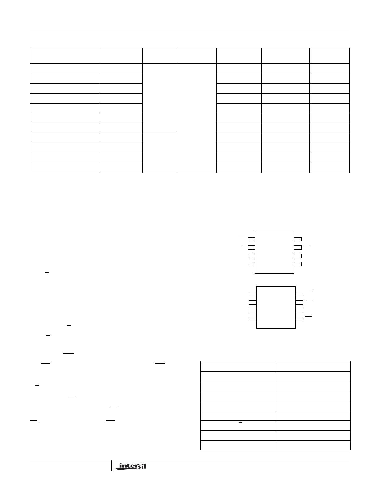
Block Diagram
U/D
INC
CS
5-Bit
Up/Down
Counter
FN8178.2
Features
• Solid State Potentiometer
•32 Taps
•10kΩ End to End Resistance
• Three-Wire Up/Down Serial Interface
• Wiper Resistance, 40Ω Typical
• Nonvolatile Storage and Recall on Power-up of Wiper
Position Standby Current < 500µA Max (Total Package)
•VCC = 3V to 5.5V Operation
• 100 Year Data Retention
• Offered in 8 Ld MSOP, SOIC and PDIP Packages
• Pb-Free Plus Anneal Available (RoHS Compliant)
31
30
VH/R
H
29
One
of
28
Transfer
Gates
2
1
0
Resistor
Array
V
L/RL
VW/R
W
5-Bit
Nonvolatile
Memory
Thirty-Two
Decoder
Store and
Recall
Control
Circuitry
V
CC
V
SS
1
CAUTION: These devices are sensitive to electrostatic discharge; follow proper IC Handling Procedures.
1-888-INTERSIL or 1-888-468-3774
XDCP is a trademark of Intersil Americas Inc. Copyright Intersil Americas Inc. 2005, 2006. All Rights Reserved
| Intersil (and design) is a registered trademark of Intersil Americas Inc.
All other trademarks mentioned are the property of their respective owners.
Ordering Information
www.BDTIC.com/Intersil
X9314
V
RANGE
PART NUMBER PART MARKING
X9314WMI* 14WI 5 ±10% 10 -40 to +85 8 Ld MSOP M8.118
X9314WP X9314WP 0 to +70 8 Ld PDIP MDP0031
X9314WPI X9314WP I -40 to +85 8 Ld PDIP MDP0031
X9314WS* X9314W 0 to +70 8 Ld SOIC M8.15
X9314WSI* X9314W I -40 to +85 8 Ld SOIC M8.15
X9314WSIZ (Note) X9314W ZI -40 to +85 8 Ld SOIC (Pb-free) M8.15
X9314WSZ* (Note) X9314W Z 0 to +70 8 Ld SOIC (Pb-free) M8.15
X9314WMI-3* AAY 3 to 5.5 -40 to +85 8 Ld MSOP M8.118
X9314WMIZ-3* (Note) DEX -40 to +85 8 Ld MSOP (Pb-free) M8.118
X9314WS-3* X9314W D 0 to +70 8 Ld SOIC M8.15
X9314WSZ-3* (Note) X9314W ZD 0 to +70 8 Ld SOIC (Pb-free) M8.15
*Add "T1" suffix for tape and reel.
NOTE: Intersil Pb-free plus anneal products employ special Pb-free material sets; molding compounds/die attach materials and 100% matte tin plate
termination finish, which are RoHS compliant and compatible with both SnPb and Pb-free soldering operations. Intersil Pb-free products are MSL
classified at Pb-free peak reflow temperatures that meet or exceed the Pb-free requirements of IPC/JEDEC J STD-020.
CC
(V)
Pin Descriptions
VH/RH and VL/R
The high (V
L
) and low (VL/RL) terminals of the X9314
H/RH
R
TOTAL
(kΩ)
Pin Configuration
are equivalent to the fixed terminals of a mechanical
potentiometer. The minimum voltage is –5V and the
maximum is +5V. It should be noted that the terminology of
V
and VH/RH references the relative position of the
L/RL
terminal in relation to wiper movement direction selected by
the U/D
VW/R
V
input and not the voltage potential on the terminal.
W
is the wiper terminal, equivalent to the movable
W/RW
terminal of a mechanical potentiometer. The position of the
wiper within the array is determined by the control inputs.
The wiper terminal series resistance is typically 40Ω.
TEMP RANGE
(°C) PACKAGE
8 LD PDIP/SOIC
INC
U/D
VH/R
V
VH/R
V
VW/R
VL/R
SS
SS
1
2
X9314
3
H
4
8 LD MSOP
H
1
2
3
W
4
L
X9314
PKG.
DWG. #
V
CC
CS
V
L/RL
V
W/RW
U/D
INC
V
CC
CS
8
7
6
5
8
7
6
5
Up/Down (U/D)
The U/D input controls the direction of the wiper movement
and whether the counter is incremented or decremented.
Increment (INC)
The INC input is negative-edge triggered. Toggling INC will
move the wiper and either increment or decrement the
counter in the direction indicated by the logic level on the
U/D
input.
Chip Select (CS)
The device is selected when the CS input is LOW. The
current counter value is stored in nonvolatile memory when
CS
is returned HIGH while the INC input is also HIGH. After
the store operation is complete the X9314 will be placed in
the low power standby mode until the device is selected
once again.
Pin Names
SYMBOL DESCRIPTION
V
V
W/RW
VL/R
V
V
H/RH
L
SS
CC
U/D
INC Increment Input
CS Chip Select Input
High Terminal
Wiper Terminal
Low Terminal
Ground
Supply Voltage
Up/Down Input
2
FN8178.2
September 5, 2006
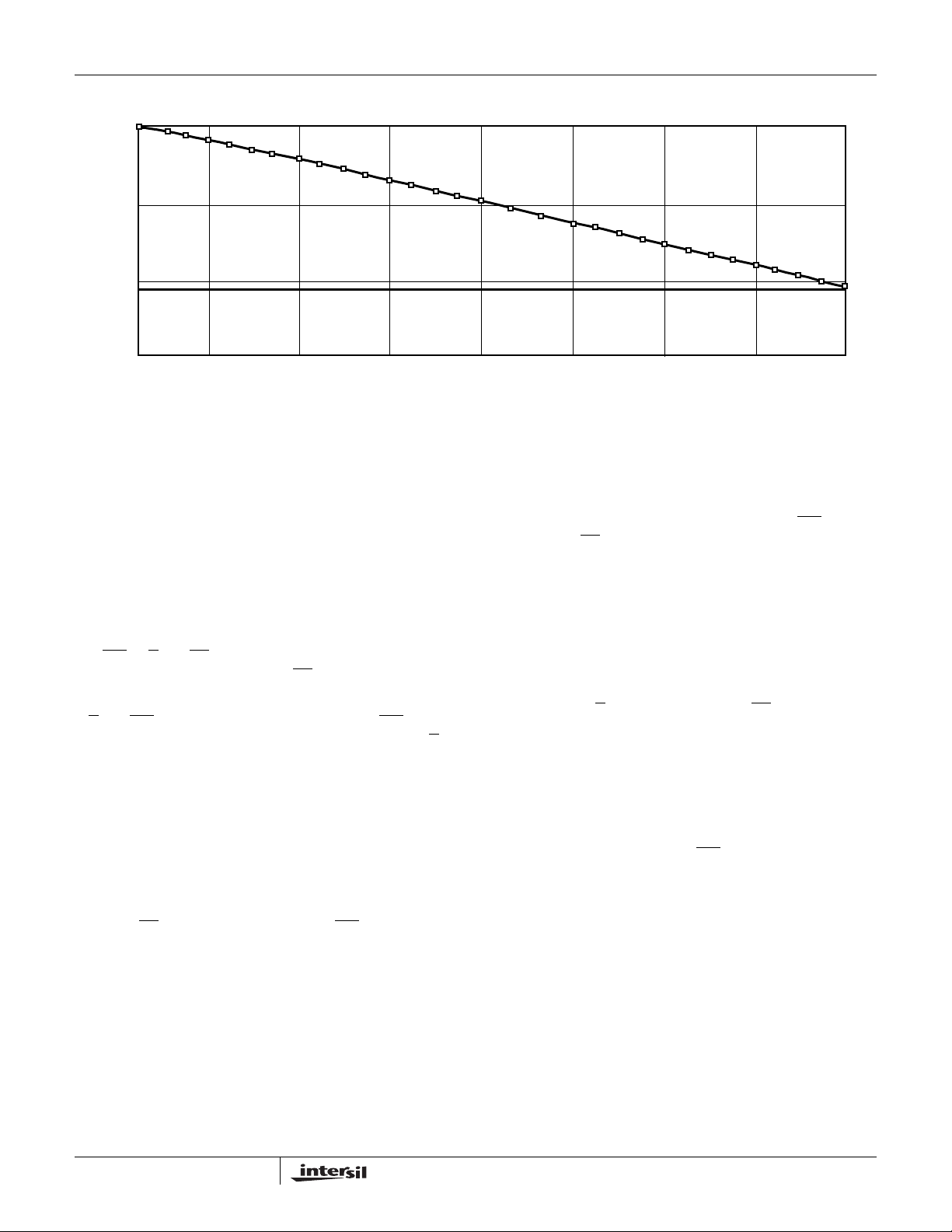
Typical Attenuation Characteristics (dB)
www.BDTIC.com/Intersil
0
-20
-40
Attenuation (dB)
-43.5
X9314
-60
Principles of Operation
There are three sections of the X9314: the input control,
counter and decode section; the nonvolatile memory; and the
resistor array. The input control section operates just like an
up/down counter. The output of this counter is decoded to turn
on a single electronic switch connecting a point on the resistor
array to the wiper output. Under the proper conditions the
contents of the counter can be stored in nonvolatile memory
and retained for future use. The resistor array is comprised of
31 individual resistors connected in series. At either end of the
array and between each resistor is an electronic switch that
transfers the potential at that point to the wiper.
The INC
wiper along the resistor array. With CS
is selected and enabled to respond to the
U/D
increment or decrement (depending on the state of the U/D
input) a five bit counter. The output of this counter is
decoded to select one of thirty-two wiper positions along the
resistive array.
The wiper, when at either fixed terminal, acts like its
mechanical equivalent and does not move beyond the last
position. That is, the counter does not wrap around when
clocked to either extreme.
The value of the counter is stored in nonvolatile memory
whenever CS
HIGH.
When the X9314 is powered-down, the last counter position
stored will be maintained in the nonvolatile memory. When
power is restored, the contents of the memory are recalled
and the counter is reset to the value last stored.
, U/D and CS inputs control the movement of the
set LOW the X9314
and INC inputs. HIGH to LOW transitions on INC will
transistions HIGH while the INC input is also
1620242831
Tap Position
12
48
0
Operation Notes
The system may select the X9314, move the wiper and
deselect the device without having to store the latest wiper
position in nonvolatile memory. The wiper
movement is performed as described above; once the new
position is reached, the system would keep the INC
while taking CS HIGH. The new wiper position would be
maintained until changed by the system or until a powerup/down cycle recalled the previously stored data.
This would allow the system to always power-up to a preset
value stored in nonvolatile memory; then during system
operation minor adjustments could be made. The
adjustments might be based on user preference, system
parameter changes due to temperature drift, etc.
The state of U/D
This allows the host system to enable the X9314 and then
move the wiper up and down until the proper trim is attained.
tIW/R
TOTAL
The electronic switches on the X9314 operate in a “make
before break” mode when the wiper changes tap positions. If
the wiper is moved several positions multiple taps are
connected to the wiper for t
R
a significant amount if the wiper is moved several positions.
value for the device can temporarily be reduced by
TOTAL
may be changed while CS remains LOW.
(INC to VW change). The
IW
LOW
Power-up and Down Requirement
The are no restrictions on the sequencing of VCC and the
voltages applied to the potentiometer pins during power-up
or power-down conditions. During power-up, the data sheet
parameters for the DCP do not fully apply until 1 millisecond
after V
always in effect.
reaches its final value. The VCC ramp rate spec is
CC
3
FN8178.2
September 5, 2006

X9314
www.BDTIC.com/Intersil
Absolute Maximum Ratings Recommended Operating Conditions
Temperature under bias. . . . . . . . . . . . . . . . . . . . . .-65°C to +135°C
Storage temperature . . . . . . . . . . . . . . . . . . . . . . . .-65°C to +150°C
Voltage on CS
V
CC
Voltage on V
to V
∆V = |V
Lead temperature (soldering 10s) . . . . . . . . . . . . . . . . . . . . .+300°C
Wiper current . . . . . . . . . . . . . . . . . . . . . . . . . . . . . . . . . . . . . . ±1mA
(10s) . . . . . . . . . . . . . . . . . . . . . . . . . . . . . . . . . . . . . . . . .±8.8mA
I
W
CAUTION: Stresses above those listed under “Absolute Maximum Ratings” may cause permanent damage to the device. This is a stress rating only; the functional
operation of the device (at these or any other conditions above those listed in the operational sections of this specification) is not implied. Exposure to absolute maximum
rating conditions for extended periods may a ffe ct d evice reli abi lit y.
, INC, U/D, and
with respect to VSS . . . . . . . . . . . . . . . . . . . . . . . -1V to +7V
. . . . . . . . . . . . . . . . . . . . . . . . . . . . . . . . . . . . . . -8V to +8V
SS
H
and VL/RL referenced
H/RH
/RH - VL/RL| . . . . . . . . . . . . . . . . . . . . . . . . . . . . . . . . .10V
Potentiometer Characteristics (Over recommended operating conditions unless otherwise stated.)
SYMBOL PARAMETER TEST CONDITIONS/NOTES
R
TOTAL
V
VL/RL
R
I
W
C
H/CL/CW
End to End Resistance Tolerance ±20 %
Terminal Voltage -5 +5 V
V
H/RH
VL/RL Terminal Voltage -5 +5 V
Power Rating at +25°C 10 mW
Wiper Resistance IW = ±1mA, VCC = 5V 40 100 Ω
W
Wiper Current ±4.4 mA
Noise Ref: 1kHz -120 dBV
Relative variation. Error in step size
between taps.
Temperature Coefficient for -40°C to +85°C ±600 ppm/°C
R
TOTAL
Ratiometric Temperature Coefficient ±20 ppm/°C
Potentiometer Capacitance See Circuit #3 10/10/25 pF
log (R
w(n)
Temperature (Commercial) . . . . . . . . . . . . . . . . . . . . . 0°C to +70°C
Temperature (Industrial). . . . . . . . . . . . . . . . . . . . . . .-40°C to +85°C
) Limits
CC
LIMITS
MIN TYP MAX UNITS
0.07 + 0.003
0.003
) - log R
Supply Voltage (V
X9314. . . . . . . . . . . . . . . . . . . . . . . . . . . . . . . . . . . . . . . 5V ± 10%
X9314-2.7. . . . . . . . . . . . . . . . . . . . . . . . . . . . . . . . . . . 3V to 5.5V
) 0.07-
w(n - 1)
NOTE:
1. This parameter is periodically sampled and not 100% tested.
4
FN8178.2
September 5, 2006

X9314
www.BDTIC.com/Intersil
DC Electrical Specifications
(Over recommended operating conditions unless otherwise specified.)
SYMBOL PARAMETER TEST CONDITIONS
I
CC
I
SB
I
V
V
C
IN
VCC Active Current CS = VIL, U/D = VIL or VIH and
= 0.4V/2.4V @ max. t
INC
Standby Supply Current CS = VCC - 0.3V, U/D and INC =VSS or
V
- 0.3V
CC
CS, INC, U/D Input Leakage Current VIN = VSS to V
LI
CS, INC, U/D Input HIGH Voltage 2 VCC + 1 V
IH
CS, INC, U/D Input LOW Voltage -1 0.8 V
IL
(3)
CS, INC, U/D Input Capacitance VCC = 5V, VIN = VSS, TA = +25°C, f = 1MHz 10 pF
CC
Standard Parts
PART NUMBER MAXIMUM RESISTANCE WIPER INCREMENTS MINIMUM RESISTANCE
X9314W 10kΩ Log Taper 40Ω
NOTES:
2. Typical values are for T
3. This parameter is periodically sampled and not 100% tested.
= +25°C and nominal supply voltage.
A
CYC
LIMITS
(2)
MAX
UNITSMIN TYP
13mA
500 µA
±10 µA
Test Circuit #1 Test Circuit #2 Circuit #3 SPICE Macromodel
10pF
Macro Model
R
TOTAL
C
H
R
C
W
25pF
W
Will be
steady
Will change
from Low to
High
Will change
from High to
Low
Changing:
State Not
Known
is High
Impedance
C
VH/R
H
Test Point
VW/R
W
VL/R
L
A.C. Conditions of Test
INPUT PULSE LEVELS 0V to 3V
Input rise and fall times 10ns
Input reference levels 1.5V
Mode Selection
CS INC U/D MODE
L H Wiper up
L L Wiper down
H X Store wiper position
H X X Standby
L X No store, return to standby
VH/R
VL/R
H
VW/R
L
Test Point
W
Force
Current
SYMBOL TABLE
WAVEFORM INPUTS OUTPUTS
R
H
Must be
steady
May change
from Low to
High
May change
from High to
Low
Don’t Care:
Changes
Allowed
N/A Center Line
L
10pF
R
L
5
FN8178.2
September 5, 2006

X9314
www.BDTIC.com/Intersil
AC Electrical Specifications (Over recommended operating conditions unless otherwise specified)
LIMITS
SYMBOL PARAMETER
t
Cl
t
lD
t
DI
t
t
lH
t
lC
t
CPH
t
IW
t
CYC
tR, t
t
PU
t
R VCC
lL
(5)
F
(5)
CS to INC Setup 100 ns
INC HIGH to U/D Change 100 ns
U/D to INC Setup 2.9 µs
INC LOW Period 1 µs
INC HIGH Period 1 µs
INC Inactive to CS Inactive 1 µs
CS Deselect Time 20 ms
INC to VW Change 100 500 µs
INC Cycle Time 4 µs
INC Input Rise and Fall Time 500 µs
Power-up to Wiper Stable 500 µs
VCC Power-up Rate 0.2 50 mV/µs
A.C. Timing
(4)
MAX
UNITSMIN TYP
CS
t
CYC
t
t
CI
INC
U/D
V
W
NOTES:
4. Typical values are for T
5. This parameter is periodically sampled and not 100% tested.
6. MI in the A.C. timing diagram refers to the minimum incremental change in the V
= +25°C and nominal supply voltage.
A
IL
t
IW
t
IH
t
IDtDI
MI
(6)
t
IC
t
CPH
90% 90%
10%
t
F
output due to a change in the wiper position.
W
t
R
6
FN8178.2
September 5, 2006

X9314
www.BDTIC.com/Intersil
Mini Small Outline Plastic Packages (MSOP)
N
EE1
INDEX
AREA
AA1A2
TOP VIEW
-H-
SIDE VIEW
12
b
e
D
NOTES:
1. These package dimensions are within allowable dimensions of
JEDEC MO-187BA.
2. Dimensioning and tolerancing per ANSI Y14.5M-1994.
3. Dimension “D” does not include mold flash, protrusions or gate
burrs and are measured at Datum Plane. Mold flash, protrusion
and gate burrs shall not exceed 0.15mm (0.006 inch) per side.
4. Dimension “E1” does not include interlead flash or protrusions
and are measured at Datum Plane. Interlead flash and
protrusions shall not exceed 0.15mm (0.006 inch) per side.
5. Formed leads shall be planar with respect to one another within
0.10mm (0.004) at seating Plane.
6. “L” is the length of terminal for soldering to a substrate.
7. “N” is the number of terminal positions.
8. Terminal numbers are shown for reference only.
9. Dimension “b” does not include dambar protrusion. Allowable
dambar protrusion shall be 0.08mm (0.003 inch) total in excess
of “b” dimension at maximum material condition. Minimum space
between protrusion and adjacent lead is 0.07mm (0.0027 inch).
- H -
-A -
.
10. Datums and to be determined at Datum plane
11. Controlling dimension: MILLIMETER. Converted inch dimensions are for reference only.
-B-
0.20 (0.008) A
GAUGE
PLANE
SEATING
PLANE
0.10 (0.004) C
-A-
0.20 (0.008) C
- B -
0.25
(0.010)
-C-
SEATING
PLANE
a
0.20 (0.008) C
- H -
B
4X θ
C
D
4X θ
L1
C
L
E
1
END VIEW
R1
R
L
C
-B-
M8.118 (JEDEC MO-187AA)
8 LEAD MINI SMALL OUTLINE PLASTIC PACKAGE
INCHES MILLIMETERS
SYMBOL
A 0.037 0.043 0.94 1.10 -
A1 0.002 0.006 0.05 0.15 -
A2 0.030 0.037 0.75 0.95 -
b 0.010 0.014 0.25 0.36 9
c 0.004 0.008 0.09 0.20 -
D 0.116 0.120 2.95 3.05 3
E1 0.116 0.120 2.95 3.05 4
e 0.026 BSC 0.65 BSC -
E 0.187 0.199 4.75 5.05 -
L 0.016 0.028 0.40 0.70 6
L1 0.037 REF 0.95 REF -
N8 87
R 0.003 - 0.07 - -
R1 0.003 - 0.07 - -
05
α
o
o
0
15
o
o
6
o
5
o
0
15
o
o
6
Rev. 2 01/03
NOTESMIN MAX MIN MAX
-
-
7
FN8178.2
September 5, 2006

Small Outline Plastic Packages (SOIC)
www.BDTIC.com/Intersil
X9314
N
INDEX
AREA
123
-A-
E
-B-
SEATING PLANE
D
A
-C-
0.25(0.010) BM M
H
L
h x 45°
α
e
B
0.25(0.010) C AM BS
NOTES:
1. Symbols are defined in the “MO Series Symbol List” in Section 2.2 of
Publication Number 95.
2. Dimensioning and tolerancing per ANSI Y14.5M-1982.
3. Dimension “D” does not include mold flash, protrusions or gate burrs.
Mold flash, protrusion and gate burrs shall not exceed 0.15mm (0.006
inch) per side.
4. Dimension “E” does not include interlead flash or protrusions. Interlead flash and protrusions shall not exceed 0.25mm (0.010 inch) per
side.
5. The chamfer on the body is optional. If it is not present, a visual index
feature must be located within the crosshatched area.
6. “L” is the length of terminal for soldering to a substrate.
7. “N” is the number of terminal positions.
8. Terminal numbers are shown for reference only.
9. The lead width “B”, as measured 0.36mm (0.014 inch) or greater
above the seating plane, shall not exceed a maximum value of
0.61mm (0.024 inch).
10. Controlling dimension: MILLIMETER. Converted inch dimensions
are not necessarily exact.
M
A1
C
0.10(0.004)
M8.15 (JEDEC MS-012-AA ISSUE C)
8 LEAD NARROW BODY SMALL OUTLINE PLASTIC PACKAGE
INCHES MILLIMETERS
SYMBOL
A 0.0532 0.0688 1.35 1.75 -
A1 0.0040 0.0098 0.10 0.25 -
B 0.013 0.020 0.33 0.51 9
C 0.0075 0.0098 0.19 0.25 -
D 0.1890 0.1968 4.80 5.00 3
E 0.1497 0.1574 3.80 4.00 4
e 0.050 BSC 1.27 BSC -
H 0.2284 0.2440 5.80 6.20 -
h 0.0099 0.0196 0.25 0.50 5
L 0.016 0.050 0.40 1.27 6
N8 87
α
0° 8° 0° 8° -
NOTESMIN MAX MIN MAX
Rev. 1 6/05
8
FN8178.2
September 5, 2006

Plastic Dual-In-Line Packages (PDIP)
www.BDTIC.com/Intersil
X9314
SEATING
PLANE
D
A2
A
L
L
e
b
A1
NOTE 5
c
E
eA
eB
N
PIN #1
E1
INDEX
12 N/2
b2
MDP0031
PLASTIC DUAL-IN-LINE PACKAGE
SYMBOL PDIP8 PDIP14 PDIP16 PDIP18 PDIP20 TOLERANCE NOTES
A 0.210 0.210 0.210 0.210 0.210 MAX
A1 0.015 0.015 0.015 0.015 0.015 MIN
A2 0.130 0.130 0.130 0.130 0.130 ±0.005
b 0.018 0.018 0.018 0.018 0.018 ±0.002
b2 0.060 0.060 0.060 0.060 0.060 +0.010/-0.015
c 0.010 0.010 0.010 0.010 0.010 +0.004/-0.002
D 0.375 0.750 0.750 0.890 1.020 ±0.010 1
E 0.310 0.310 0.310 0.310 0.310 +0.015/-0.010
E1 0.250 0.250 0.250 0.250 0.250 ±0.005 2
e 0.100 0.100 0.100 0.100 0.100 Basic
eA 0.300 0.300 0.300 0.300 0.300 Basic
eB 0.345 0.345 0.345 0.345 0.345 ±0.025
L 0.125 0.125 0.125 0.125 0.125 ±0.010
N 8 14 16 18 20 Reference
NOTES:
1. Plastic or metal protrusions of 0.010” maximum per side are not included.
2. Plastic interlead protrusions of 0.010” maximum per side are not included.
3. Dimensions E and eA are measured with the leads constrained perpendicular to the seating plane.
4. Dimension eB is measured with the lead tips unconstrained.
5. 8 and 16 lead packages have half end-leads as shown.
Rev. B 2/99
All Intersil U.S. products are manufactured, assembled and tested utilizing ISO9000 quality systems.
Intersil Corporation’s quality certifications can be viewed at www.intersil.com/design/quality
Intersil products are sold by description only. Intersil Corporation reserves the right to make changes in circuit design, software and/or specifications at any time without
notice. Accordingly, the reader is cautioned to verify that data sheets are current before placing orders. Information furnished by Intersil is believed to be accurate and
reliable. However, no responsibility is assumed by Intersil or its subsidiaries for its use; nor for any infringements of patents or other rights of third parties which may result
from its use. No license is granted by implic atio n or other wise u nde r any p a tent or patent rights of Intersil or its subsidi aries.
For information regarding Intersil Corporation and its products, see www.intersil.com
9
FN8178.2
September 5, 2006
 Loading...