

®
www.BDTIC.com/Intersil
X9241A
Quad Digital Controlled Potentionmeters (XDCP™)
Data Sheet FN8164.6August 31, 2007
Non-Volatile/Low Power/2-Wire/64 Taps
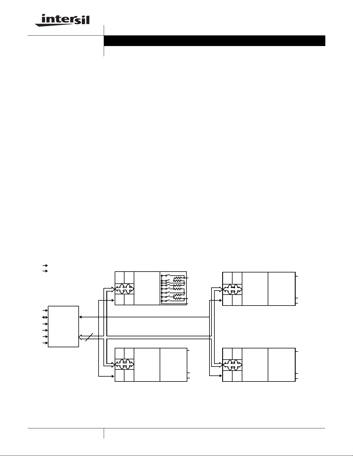
The X9241A integrates four digitally controlled
potentiometers (XDCP) on a monolithic CMOS integrated
microcircuit.
The digitally controlled potentiometer is implemented using
63 resistive elements in a series array. Between each
element are tap points connected to the wiper terminal
through switches. The position of the wiper on the array is
controlled by the user through the 2-wire bus interface. Each
potentiometer has associated with it a volatile Wiper Counter
Register (WCR) and 4 nonvolatile Data Registers
(DR0:DR3) that can be directly written to and read by the
user. The contents of the WCR controls the position of the
wiper on the resistor array through the switches. Power up
recalls the contents of DR0 to the WCR.
The XDCP can be used as a three-terminal potentiometer or
as a two-terminal variable resistor in a wide variety of
applications including control, parameter adjustments, and
signal processing.
Features
• Four potentiometers in one package
• 2-wire serial interface
• Register oriented format
- Direct read/write/transfer of wiper positions
- Store as many as four positions per potentiometer
• Terminal Voltages: +5V, -3.0V
• Cascade resistor arrays
• Low power CMOS
• High Reliability
- Endurance–100,000 data changes per bit per register
- Register data retention–100 years
• 16-bytes of nonvolatile memory
• 3 resistor array values
-2kΩ, 10kΩ, 50kΩ or combination
- Cascadable for values of 4kΩ to 200kΩ
• Resolution: 64 taps each pot
• 20 Ld plastic DIP, 20 Ld TSSOP and 20 Ld SOIC
packages
• Pb-free available (RoHS compliant)
Block Diagram
V
CC
V
SS
SCL
SDA
A0
A1
A2
A3
INTERFACE
AND
CONTROL
CIRCUITRY
DATA
/
V
R0
R1
WIPER
COUNTER
REGISTER
R3
R1
R3
(WCR)
WIPER
COUNTER
REGISTER
(WCR)
REGISTER
ARRAY
POT 1
R2
8
R0
R2
V
H0/RH0
VL0/R
VW0/R
V
H1/RH1
VL1/R
VW1/R
R0
R1
WIPER
COUNTER
REGISTER
L0
W0
L1
W1
R2
R0
R2
R3
R1
R3
(WCR)
WIPER
COUNTER
REGISTER
(WCR)
REGISTER
ARRAY
POT 2
REGISTER
ARRAY
POT 3
H2
R
H2
V
L2/RL2
VW2/R
VH3/R
VL3/R
VW3/R
W2
H3
L3
W3
1
XDCP is a trademark of Intersil Americas Inc. Copyright Intersil Americas Inc. 2005, 2006, 2007. All Rights Reserved
CAUTION: These devices are sensitive to electrostatic discharge; follow proper IC Handling Procedures.
1-888-INTERSIL or 1-888-468-3774
| Intersil (and design) is a registered trademark of Intersil Americas Inc.
All other trademarks mentioned are the property of their respective owners.
X9241A
www.BDTIC.com/Intersil
Ordering Information
POTENTIOMETER
LIMITS
V
CC
PART NUMBER PART MARKING
X9241AMP X9241AMP 5 ±10% 2/10/50
X9241AMPZ (Note) X9241AMPZ 0 to +70 20 Ld PDIP*** (Pb-free)
X9241AMPI X9241AMPI -40 to +85 20 Ld PDIP
X9241AMPIZ (Note) X9241AMPIZ -40 to +85 20 Ld PDIP*** (Pb-free)
X9241AMS* X9241AMS 0 to +70 20 Ld SOIC
X9241AMSZ* (Note) X9241AMS Z 0 to +70 20 Ld SOIC (Pb-free)
X9241AMSI*
X9241AMSIZ* (Note) X9241AMSI Z -40 to +85 20 Ld SOIC (Pb-free)
X9241AMV X9241AM V 0 to +70 20 Ld TSSOP
X9241AMVZ (Note) X9241AM VZ 0 to +70 20 Ld TSSOP (Pb-free)
X9241AMVI*
X9241AMVIZ* (Note) X9241AM VIZ -40 to +85 20 Ld TSSOP (Pb-free)
X9241AWP X9241AWP 10
X9241AWPI X9241AWPI -40 to +85 20 Ld PDIP
X9241AWPIZ (Note) X9241AWPIZ -40 to +85 20 Ld PDIP*** (Pb-free)
X9241AWS*
X9241AWSZ* (Note) X9241AWS Z 0 to +70 20 Ld SOIC (Pb-free)
X9241AWSI*
X9241AWSIZ* (Note) X9241AWSI Z -40 to +85 20 Ld SOIC (Pb-free)
X9241AWV*
X9241AWVZ* (Note) X9241AW VZ 0 to +70 20 Ld TSSOP (Pb-free)
X9241AWVI*
X9241AWVIZ*
X9241AYP X9241AYP 2
X9241AYPZ (Note) X9241AYPZ 0 to +70 20 Ld PDIP*** (Pb-free)
X9241AYS* X9241AYS 0 to +70 20 Ld SOIC
X9241AYSZ* (Note) X9241AYS Z 0 to +70 20 Ld SOIC (Pb-free)
X9241AYSI* X9241AYSI -40 to +85 20 Ld SOIC
X9241AYSIZ* (Note) X9241AYSI Z -40 to +85 20 Ld SOIC (Pb-free)
X9241AYV X9241AY V 0 to +70 20 Ld TSSOP
X9241AYVZ (Note) X9241AY VZ 0 to +70 20 Ld TSSOP (Pb-free)
X9241AYVI*
X9241AYVIZ* (Note) X9241AY VIZ -40 to +85 20 Ld TSSOP (Pb-free)
,
** X9241AMSI -40 to +85 20 Ld SOIC
,
** X9241AM VI -40 to +85 20 Ld TSSOP
,
** X9241AWS 0 to +70 20 Ld SOIC
,
** X9241AWSI -40 to +85 20 Ld SOIC
,
** X9241AW V 0 to +70 20 Ld TSSOP
,
** X9241AW VI -40 to +85 20 Ld TSSOP
(Note) X9241AW VIZ -40 to +85 20 Ld TSSOP (Pb-free)
,
** X9241AY VI -40 to +85 20 Ld TSSOP
(V)
ORGANIZATION
Pot 0 = 2k
Pot 1 = 10k
Pot 2 = 10k
Pot 3 = 50k
Pot 0 = 10k
Pot 1 = 10k
Pot 2 = 10k
Pot 3 = 10k
Pot 0 = 2k
Pot 1 = 2k
Pot 2 = 2k
Pot 3 = 2k
(k)
TEMP RANGE
(°C) PACKAGE
0 to +70 20 Ld PDIP
0 to +70 20 Ld PDIP
0 to +70 20 Ld PDIP
2
FN8164.6
August 31, 2007
X9241A
www.BDTIC.com/Intersil
Ordering Information (Continued)
V
LIMITS
PART NUMBER PART MARKING
X9241AUP X9241AUP 5 ±10% 50
X9241AUPZ (Note) X9241AUPZ 0 to +70 20 Ld PDIP*** (Pb-free)
X9241AUPI X9241AUPI -40 to +85 20 Ld PDIP
X9241AUPIZ (Note) X9241AUPIZ -40 to +85 20 Ld PDIP*** (Pb-free)
X9241AUS X9241AUS 0 to +70 20 Ld SOIC
X9241AUSZ* (Note) X9241AUS Z 0 to +70 20 Ld SOIC (Pb-free)
X9241AUSI*
X9241AUSIZ* (Note) X9241AUSI Z -40 to +85 20 Ld SOIC (Pb-free)
X9241AUV* X9241AU V 0 to +70 20 Ld TSSOP
X9241AUVZ* (Note) X9241AU VZ 0 to +70 20 Ld TSSOP (Pb-free)
X9241AUVI*
X9241AUVIZ* (Note) X9241AU VIZ -40 to +85 20 Ld TSSOP (Pb-free)
*Add "T1" suffix for tape and reel.
**Add “T2” suffix for tape and reel.
***Pb-free PDIPs can be used for through hole wave solder processing only. They are not intended for use in Reflow solder processing applications.
NOTE: These Intersil Pb-free plastic packaged products employ special Pb-free material sets; molding compounds/die attach materials and 100%
matte tin plate PLUS ANNEAL - e3 termination finish, which is RoHS compliant and compatible with both SnPb and Pb-free soldering operations.
Intersil Pb-free products are MSL classified at Pb-free peak reflow temperatures that meet or exceed the Pb-free requirements of IPC/JEDEC J
STD-020.
,
** X9241AUSI -40 to +85 20 Ld SOIC
,
** X9241AU VI -40 to +85 20 Ld TSSOP
CC
(V)
POTENTIOMETER
ORGANIZATION
(k)
Pot 0 = 50k
Pot 1 = 50k
Pot 2 = 50k
Pot 3 = 50k
TEMP RANGE
(°C) PACKAGE
0 to +70 20 Ld PDIP
Pin Descriptions
Host Interface Pins
Serial Clock (SCL)
The SCL input is used to clock data into and out of the
X9241A.
Serial Data (SDA)
SDA is a bidirectional pin used to transfer data into and out
of the device. It is an open drain output and may be wireORed with any number of open drain or open collector
outputs. An open drain output requires the use of a pull-up
resistor. For selecting typical values, refer to the guidelines
for calculating typical values on the bus pull-up resistors
graph.
Address
The Address inputs are used to set the least significant
4-bits of the 8-bit slave address. A match in the slave
address serial data stream must be made with the Address
input in order to initiate communication with the X9241A.
Potentiometer Pins
VH/RH(VH0/RH0 TO VH3/RH3), VL/RL (VL0/RL0 TO VL3/RL3)
The R
connections on either end of a mechanical potentiometer.
V
The wiper outputs are equivalent to the wiper output of a
mechanical potentiometer.
and RL inputs are equivalent to the terminal
H
(VW0/RW0 TO VW3/RW3)
W/RW
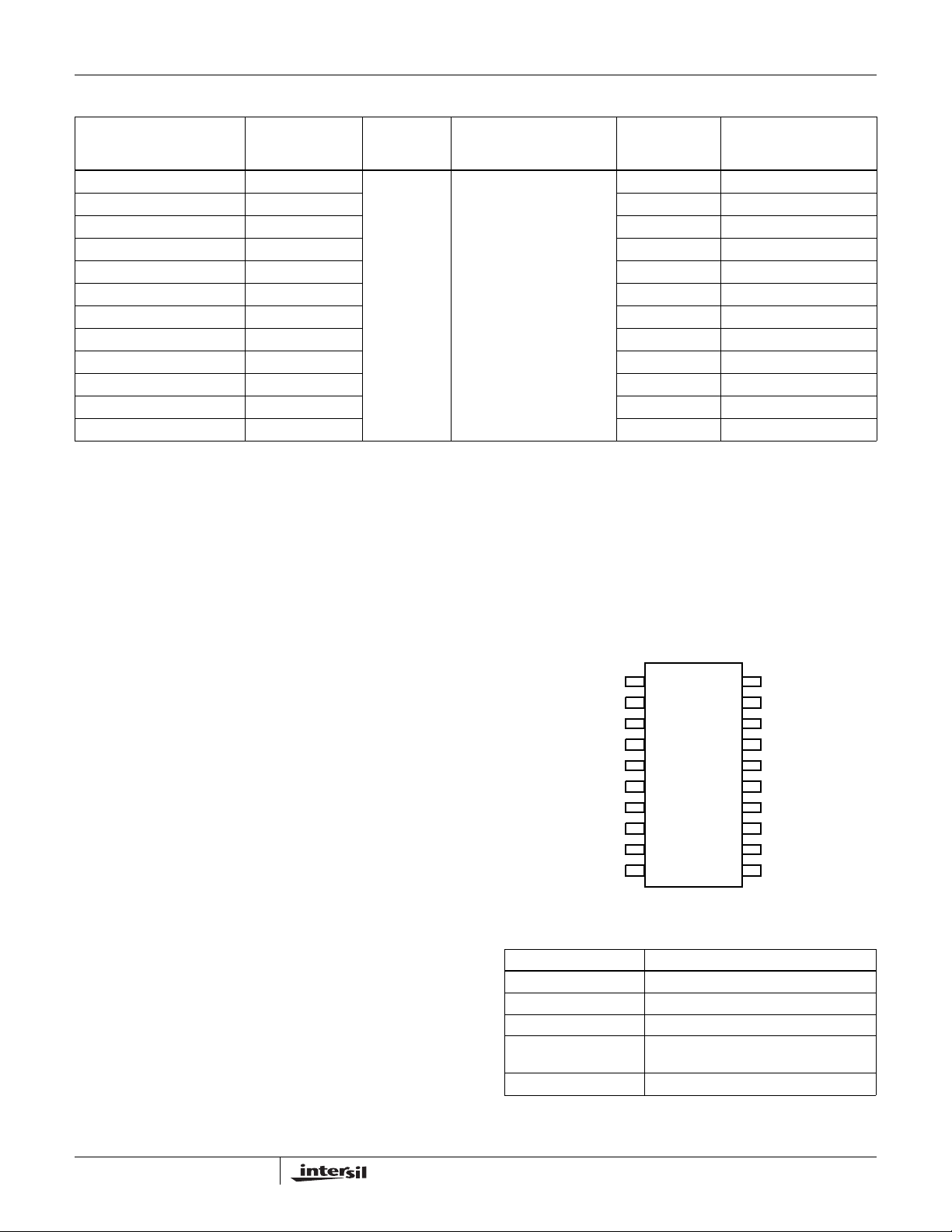
Pinout
X9241A
TOP VIEW
1
2
3
4
5
X9241A
6
7
8
9
10
(20 LD DIP, SOIC, TSSOP)
VW0/RW0
VL0/RL0
V
H0/RH0
A0
A2
VW1/RW1
V
L1/RL1
V
H1/RH1
SDA
V
SS
Pin Names
SYMBOL DESCRIPTION
SCL Serial Clock
SDA Serial Data
A0 to A3 Address
V
V
to VH3/RH3,
H0/RH0
V
to VL3/R
L0/RL0
to VW3/RW3Potentiometer Pins (wiper equivalent)
W0/RW0
Potentiometer Pins (terminal equivalent)
L3
20
19
18
17
16
15
14
13
12
11
V
CC
V
W3/RW3
V
L3/RL3
V
H3/RH3
A1
A3
SCL
VW2/RW2
V
L2/RL2
V
H2/RH2
3
FN8164.6
August 31, 2007
X9241A
www.BDTIC.com/Intersil
Principles of Operation
The X9241A is a highly integrated microcircuit incorporating
four resistor arrays, their associated registers and counters
and the serial interface logic providing direct communication
between the host and the XDCP potentiometers.
Serial Interface
The X9241A supports a bidirectional bus oriented protocol.
The protocol defines any device that sends data onto the
bus as a transmitter and the receiving device as the receiver.
The device controlling the transfer is a master and the
device being controlled is the slave. The master will always
initiate data transfers and provide the clock for both transmit
and receive operations. Therefore, the X9241A will be
considered a slave device in all applications.
Clock and Data Conventions
Data states on the SDA line can change only during SCL
LOW periods (t
are reserved for indicating start and stop conditions.
Start Condition
All commands to the X9241A are preceded by the start
condition, which is a HIGH to LOW transition of SDA while
SCL is HIGH (t
SDA and SCL lines for the start condition and will not
respond to any command until this condition is met.
). SDA state changes during SCL HIGH
LOW
). The X9241A continuously monitors the
HIGH
At both ends of each array and between each resistor
segment is a FET switch connected to the wiper (V
output. Within each individual array only one switch may be
turned on at a time. These switches are controlled by the
Wiper Counter Register (WCR). The 6 least significant bits of
the WCR are decoded to select, and enable, 1 of 64
switches.
The WCR may be written directly, or it can be changed by
transferring the contents of one of four associated Data
Registers into the WCR. These Data Registers and the WCR
can be read and written by the host system.
W/RW
)
Device Addressing
Following a start condition the master must output the
address of the slave it is accessing. The most significant
4-bits of the slave address are the device type identifier
(refer to Figure 1). For the X9241A, this is fixed as 0101[B].
DEVICE TYPE
IDENTIFIER
10 0 A3 A2 A1 A0
FIGURE 1. SLAVE ADDRESS
1
DEVICE ADDRESS
Stop Condition
All communications must be terminated by a stop condition,
which is a LOW to HIGH transition of SDA while SCL is
HIGH.
Acknowledge
Acknowledge is a software convention used to provide a
positive handshake between the master and slave devices
on the bus to indicate the successful receipt of data. The
transmitting device, either the master or the slave, will
release the SDA bus after transmitting 8-bits. The master
generates a ninth clock cycle and during this period the
receiver pulls the SDA line LOW to acknowledge that it
successfully received the 8-bits of data. See Figure 7.
The X9241A will respond with an acknowledge after
recognition of a start condition and its slave address and
once again after successful receipt of the command byte. If
the command is followed by a data byte the X9241A will
respond with a final acknowledge.
Array Description
The X9241A is comprised of four resistor arrays. Each array
contains 63 discrete resistive segments that are connected
in series. The physical ends of each array are equivalent to
the fixed terminals of a mechanical potentiometer (V
and V
L/RL
inputs).
H/RH
The next 4-bits of the slave address are the device address.
The physical device address is defined by the state of the A0
to A3 inputs. The X9241A compares the serial data stream
with the address input state; a successful compare of all 4
address bits is required for the X9241A to respond with an
acknowledge.
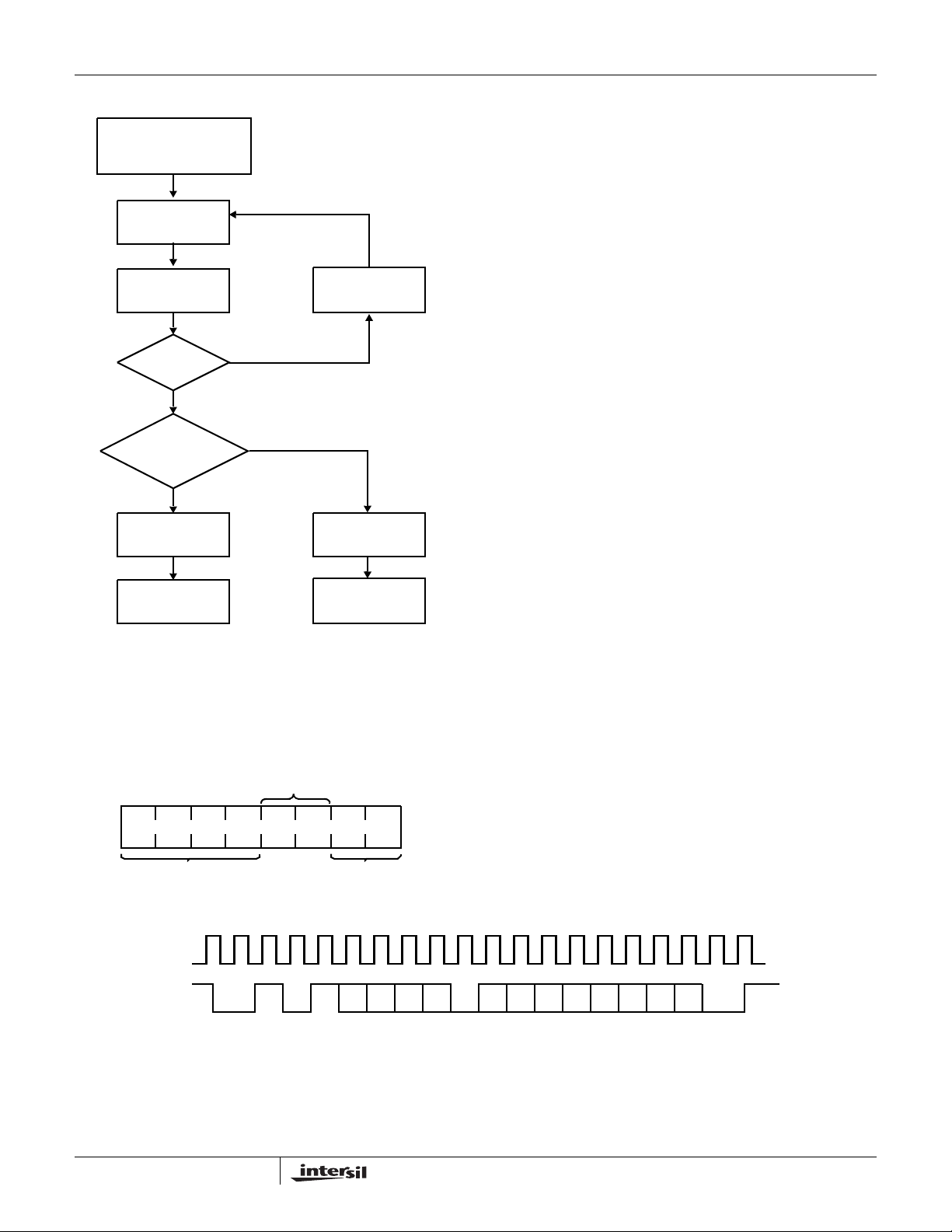
Acknowledge Polling
The disabling of the inputs, during the internal nonvolatile
write operation, can be used to take advantage of the typical
5ms EEPROM write cycle time. Once the stop condition is
issued to indicate the end of the nonvolatile write command,
the X9241A initiates the internal write cycle. ACK polling can
be initiated immediately. This involves issuing the start
condition followed by the device slave address. If the
X9241A is still busy with the write operation, no ACK will be
returned. If the X9241A has completed the write operation,
an ACK will be returned and the master can then proceed
with the next operation.
4
FN8164.6
August 31, 2007
X9241A
www.BDTIC.com/Intersil
Flow 1. ACK Polling Sequence
NONVOLATILE WRITE
COMMAND COMPLETED
ENTER ACK POLLING
ISSUE
START
ISSUE SLAVE
ADDRESS
ACK
RETURNED?
YES
FURTHER
OPERATION?
YES
ISSUE
INSTRUCTION
PROCEED
NO
NO
ISSUE STOP
ISSUE STOP
PROCEED
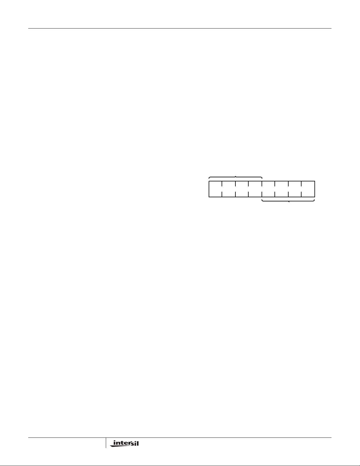
The 4 high order bits define the instruction. The next 2-bits
(P1 and P0) select which one of the four potentiometers is to
be affected by the instruction. The last 2-bits (R1 and R0)
select one of the four registers that are to be acted upon
when a register oriented instruction is issued.
Four of the nine instructions end with the transmission of the
instruction byte. The basic sequence is illustrated in Figure 3.
These two-byte instructions exchange data between the WCR
and one of the data registers. A transfer from a Data R egister
to a WCR is essentially a write to a static RAM. The response
of the wiper to this action will be delayed t
STPWV
. A transfer
from WCR current wiper position to a Data Register is a write
to nonvolatile memory and takes a minimum of t
WR
to
complete. The transfer can occur between one of the four
potentiometers and one of its associated registers; or it may
occur globally , wherein the transfer occurs be tween all four of
the potentiometers and one of their associated registers.
Four instructions require a three-byte sequence to complete.
These instructions transfer data between the host and the
X9241A; either between the host and one of the Data
Registers or directly between the host and the WCR. These
instructions are: Read WCR, read the current wiper position
of the selected pot; Write WCR, change current wiper
position of the selected pot; Read Data Register, read the
contents of the selected nonvolatile register; Write Data
Register, write a new value to the selected Data Register.
The sequence of operations is shown in Figure 4.
Instruction Structure
The next byte sent to the X9241A contains the instruction
and register pointer information. The 4 most significant bits
are the instruction. The next 4-bits point to one of four pots
and when applicable they point to one of four associated
registers. The format is in Figure 2.
POTENTIOMETER
SELECT
I1I2I3 I0 P1 P0 R1 R0
INSTRUCTIONS
FIGURE 2. INSTRUCTION BYTE FORMAT
SCL
SDA
S
0101A3A2A1A0
T
A
R
T
REGISTER
SELECT
The Increment/Decrement command is different from the
other commands. Once the command is issued and the
X9241A has responded with an acknowledge, the master
can clock the selected wiper up and/or down in one segment
steps; thereby, providing a fine tuning capability to the host.
For each SCL clock pulse (t
) while SDA is HIGH, the
HIGH
selected wiper will move one resistor segment towards the
V
terminal. Similarly, for each SCL clock pulse while
H/RH
SDA is LOW, the selected wiper will move one resistor
segment towards the V
terminal. A detailed illustration
L/RL
of the sequence and timing for this operation is shown in
Figures 5 and 6 respectively.
I3 I2 I1 I0 P1 P0 R1 R0
A
C
K
S
A
T
C
O
K
P
FIGURE 3. TWO-BYTE INSTRUCTION SEQUENCE
5
FN8164.6
August 31, 2007

SCL
www.BDTIC.com/Intersil
SDA
X9241A
SCL
SDA
INC/DEC
ISSUED
S
0 1 0 1 A3 A2 A1 A0
T
A
R
T
S
0 1 0 1 A3A2A1A0 I3 I2 I1 I0 P1 P0 R1 R0
T
A
R
T
CMD
SCL
I3 I2 I1 I0 P1 P0 R1 R0
A
C
K
DW D5 D4 D3 D2
A
CM
C
K
FIGURE 4. THREE-BYTE INSTRUCTION SEQUENCE
XX
A
C
K
A
I
C
N
K
C
1
FIGURE 5. INCREMENT/DECREMENT INSTRUCTION SEQUENCE
t
CLWV
S
D1 D0
I
N
C
2
I
D
N
E
C
C
n
1
A
T
C
O
K
P
S
D
T
E
O
C
P
n
SDA
VW/R
W
VOLTAGE OUT
FIGURE 6. INCREMENT/DECREMENT TIMING LIMITS
TABLE 1. INSTRUCTION SET
INSTRUCTION FORMAT
P
P
R
INSTRUCTION
Read WCR 1 0 0 1 1/0
3I2I1I0
(Note 1)
1
0
1/0 X
(Note 2)
R
1
0
OPERATIONI
X Read the contents of the Wiper Counter Register pointed to by P1 to P
Write WCR 1 0 1 0 1/0 1/0 X X Write new value to the Wiper Counter Register pointed to by P1 to P
Read Data
1 0 1 1 1/0 1/0 1/0 1/0 Read the contents of the Register pointed to by P1 to P0 and R1 to R
Register
Write Data
1 1 0 0 1/0 1/0 1/0 1/0 Write new value to the Register pointed to by P1 to P0 and R1 to R
Register
0
0
0
0
6
FN8164.6
August 31, 2007

X9241A
www.BDTIC.com/Intersil
TABLE 1. INSTRUCTION SET (Continued)
INSTRUCTION FORMAT
P
P
R
INSTRUCTION
XFR Data
Register to WCR
XFR WCR to
Data Register
Global XFR
Data Register to
WCR
Global XFR
WCR to Data
Register
Increment/
Decrement
Wiper
NOTES:
1. 1/0 = data is one or zero
2. X = Not applicable or don’t care; that is, a data register is not involved in the operation and need not be addressed (typical).
3I2I1I0
1 1 0 1 1/0 1/0 1/0 1/0 Transfer the contents of the Register pointed to by P
1 1 1 0 1/0 1/0 1/0 1/0 Transfer the contents of the WCR pointed to by P
0 0 0 1 X X 1/0 1/0 Transfer the contents of the Data Registers pointed to by R
1 0 0 0 X X 1/0 1/0 Transfer the contents of all WCRs to their respective data Registers
0 0 1 0 1/0 1/0 X X Enable Increment/decrement of the WCR pointed to by P
1
0
R
1
0
R
to its associated WCR
0
pointed to by R
four pots to their respective WCR
pointed to by R
to R
1
to R0 of all four pots
1
OPERATIONI
0
to P0 and R1 to
1
to P0 to the Register
1
to R0 of all
1
to P
1
0
SCL FROM
MASTER
DATA OUTPUT
FROM TRANSMITTER
DATA OUTPUT
FROM RECEIVER
STAR T
1
FIGURE 7. ACKNOWLEDGE RESPONSE FROM RECEIVER
89
ACKNOWLEDGE
7
FN8164.6
August 31, 2007

X9241A
www.BDTIC.com/Intersil
Detailed Operation
All four XDCP potentiometers share the serial interface and
share a common architecture. Each potentiometer is
comprised of a resistor array, a Wiper Counter Register and
four Data Registers. A detailed discussion of the register
organization and array operation follows.
Wiper Counter Register
The X9241A contains four volatile Wiper Counter Registers
(WCR), one for each XDCP potentiometer. The WCR can be
envisioned as a 6-bit parallel and serial load counter with its
outputs decoded to select one of sixty-four switches along its
resistor array. The contents of the WCR can be altered in
four ways: it may be written directly by the host via the Write
WCR instruction (serial load); it may be written indirectly by
transferring the contents of one of four associated Data
Registers via the XFR Data Register instruction (parallel
load); it can be modified one step at a time by the
increment/decrement instruction; finally, it is loaded with the
contents of its Data Register zero (DR0) upon power-up.
The WCR is a volatile register; that is, its contents are lost
when the X9241A is powered-down. Although the register is
automatically loaded with the value in DR0 upon power-up, it
should be noted this may be different from the value present
at power-down.
Data Registers
Each potentiometer has four nonvolatile Data Registers.
These can be read or written directly by the host and data
can be transferred between any of the four Data Registers
and the WCR. It should be noted all operations changing
data in one of these registers is a nonvolatile operation and
will take a maximum of 10ms.
If the application does not require storage of multiple
settings for the potentiometer, these registers can be used
as regular memory locations that could possibly store
system parameters or user preference data.
SERIAL DATA PATH
FROM INTERFACE
CIRCUITRY
IF WCR = 00[H] THEN VW/RW = VL/RL
IF WCR = 3F[H] THEN V
W/RW
= VH/R
REGISTER 0
8 6
REGISTER 2 REGISTER 3
H
REGISTER 1
2
MODIFIED SCL
UP/DN
SERIAL
BUS
INPUT
PARALLEL
BUS
INPUT
WIPER
COUNTER
REGISTER
INC/DEC
LOGIC
UP/DN
CLK
DW
CASCADE
CONTROL
LOGIC
CM
VH/R
H
C
O
U
N
T
E
R
D
E
C
O
D
E
V
L/RL
VW/R
W
FIGURE 8. DETAILED POTENTIOMETER BLOCK DIAGRAM
8
FN8164.6
August 31, 2007

X9241A
www.BDTIC.com/Intersil
Cascade Mode
The X9241A provides a mechanism for cascading the
arrays. That is, the sixty-three resistor elements of one array
may be cascaded (linked) with the resistor elements of an
adjacent array. The V
connected to the V
of the higher order array must be
L/RL
of the lower order array (See
H/RH
Figure 9).
Cascade Control Bits
The data byte, for the three-byte commands, contains 6-bits
(LSBs) for defining the wiper position plus 2 high order bits,
CM (Cascade Mode) and DW (Disable Wiper, normal
operation).
The state of the CM bit (bit 7 of WCR) enables or disables
cascade mode. When the CM bit of the WCR is set to “0” the
potentiometer is in the normal operation mode. When the
CM bit of the WCR is set to “1” the potentiometer is
cascaded with its adjacent higher order potentiometer. For
example; if bit 7 of WCR2 is set to “1”, pot 2 will be cascaded
to pot 3.
The state of DW enables or disables the wiper. When the
DW bit (bit 6 of the WCR) is set to “0” the wiper is enabled;
when set to “1” the wiper is disabled. If the wiper is disabled,
the wiper terminal will be electrically isolated and float.
When operating in cascade mode V
, VL/RL and the
H/RH
wiper terminals of the cascaded arrays must be electrically
connected externally. All but one of the wipers must be
disabled. The user can alter the wiper position by writing
directly to the WCR or indirectly by transferring the contents
of the Data Registers to the WCR or by using the
Increment/Decrement command.
When using the Increment/Decrement command the wiper
position will automatically transition between arrays. The
current position of the wiper can be determined by reading
the WCR registers; if the DW bit is “0”, the wiper in that array
is active. If the current wiper position is to be maintained on
power-down a global XFR WCR to Data Register command
must be issued to store the position in NV memory before
power-down.
It is possible to connect three or all four potentiometers in
cascade mode. It is also possible to connect POT 3 to POT 0
as a cascade. The requirements for external connections of
V
, VH/RH and the wipers are the same in these cases.
L/RL
EXTERNAL
=
CONNECTION
POT 0
WCR0
POT 1
WCR1
POT 2
WCR2
POT 3
WCR3
FIGURE 9. CASCADING ARRAYS
VL0/R
VH0/R
VW0/R
VL1/R
VH1/R
VW1/R
VL2/R
VH2/R
VW2/R
VL3/R
VH3/R
VW3/R
L0
H0
W0
L1
H1
W1
L2
H2
W2
L3
H3
W3
9
FN8164.6
August 31, 2007

X9241A
www.BDTIC.com/Intersil
Absolute Maximum Ratings Thermal Information
Supply Voltage (VCC) Limits
X9241A. . . . . . . . . . . . . . . . . . . . . . . . . . . . . . . . . . . . . . 5V ±10%
Max Wiper Current for 2k R
Max Wiper Current for 10k and 50k R
Voltage on SCK, SCL or any address
input with respect to V
Voltage on any V
referenced to V
ΔV = |V
(10s) . . . . . . . . . . . . . . . . . . . . . . . . . . . . . . . . . . . . . . . . . . ±6mA
I
W
Power rating (each pot) . . . . . . . . . . . . . . . . . . . . . . . . . . . . . .50mW
CAUTION: Do not operate at or near the maximum ratings listed for extended periods of time. Exposure to such conditions may adversely impact product reliability and
result in failures not covered by warranty.
- VL/RL|. . . . . . . . . . . . . . . . . . . . . . . . . . . . . . . . . .10V
H/RH
SS
, VW/RW or VL/RL
H/RH
. . . . . . . . . . . . . . . . . . . . . . . . . . . . . . +6V/-4V
SS
. . . . . . . . . . . . . . . . . . . . . . ±4mA
TOTAL
. . . . . . . . . . . . . . . . . . . . . . . -1V to +7V
. . . . . . . . . . . . . . ±3mA
TOTAL
Analog Specifications (Over recommended operating conditions unless otherwise stated).
SYMBOL PARAMETER TEST CONDITION
R
TOTAL
R
V
TERM
C
H/CL/CW
End to end resistance -20 +20 %
Wiper resistance Wiper Current = (VH - VL)/R
W
Voltage on any VH/RH, VW/RW or VL/RL Pin -3.0 +5 V
Noise Ref: 1kHz (Note 7) ≤120 dBV
Resolution (Note 7) 1.6 %
Absolute linearity (Note 3) R
Relative linearity
Temperature coefficient of R
Ratiometric temperature coefficient (Note 7) ±20 ppm/C
Potentiometer capacitances See Circuit #3 and (Note 7) 15/15/25 pF
RH, RI, RW leakage current VIN = V
l
AL
(Note 4) R
TOTAL
w(n)(actual)
- [R
w(n + 1)
(Note 7) ±300 ppm/°C
TERM
Temperature under bias. . . . . . . . . . . . . . . . . . . . . . . .-65 to +135°C
Storage temperature . . . . . . . . . . . . . . . . . . . . . . . . . .-65 to +150°C
Pb-free reflow profile . . . . . . . . . . . . . . . . . . . . . . . . . .see link below
http://www.intersil.com/pbfree/Pb-FreeReflow.asp
Recommended Operating Conditions
Temperature (Commercial) . . . . . . . . . . . . . . . . . . . . . 0°C to +70°C
Temperature (Industrial). . . . . . . . . . . . . . . . . . . . . . .-40°C to +85°C
LIMITS
MIN
(Note 11) TYP
TOTAL
- R
w(n)(expected)
w(n) + MI
. Device is in stand-by mode. 0.1 1 µA
] ±0.2 MI (Note 5)
40 130 Ω
MAX
(Note 11)
±1 MI (Note 5)
UNIT
DC Electrical Specifications (Over recommended operating conditions unless otherwise stated.)
LIMITS
MIN
SYMBOL PARAMETER TEST CONDITION
l
CC
I
SB
I
I
LO
V
V
V
NOTES:
3. Absolute Linearity is utilized to determine actual wiper voltage versus expected voltage as determined by wiper position when used as a
potentiometer.
4. Relative Linearity is utilized to determine the actual change in voltage between two successive tap positions when used as a potentiometer. It is
a measure of the error in step size.
5. MI = RTOT/63 or (R
6. Max = all four arrays cascaded together, Typical = individual array resolutions.
Supply current (active) f
VCC current (standby) SCL = SDA = VCC, Addr. = V
Input leakage current VIN = VSS to V
LI
Output leakage current V
Input HIGH voltage 2 V
IH
Input LOW voltage 0.8 V
IL
Output LOW voltage IOL = 3mA 0.4 V
OL
– RL)/63, single pot
H
= 100kHz, Write/Read to WCR,
SCL
Other Inputs = V
= VSS to V
OUT
SS
CC
CC
SS
(Note 11) TYP
200 500 µA
10
MAX
(Note 11)
3mA
10 µA
10 µA
UNIT
FN8164.6
August 31, 2007

X9241A
www.BDTIC.com/Intersil
Endurance and Data Retention
PARAMETER MIN UNIT
Minimum endurance 100,000 Data changes per bit per register
Data retention 100 Years
Capacitance
SYMBOL PARAMETER TEST CONDITION TYP UNIT
(Note 7) Input/output capacitance (SDA) V
C
I/O
C
(Note 7) Input capacitance (A0, A1, A2, A3 and SCL) VIN = 0V 12 pF
IN
Power-up Timing
MIN
SYMBOL PARAMETER
t
(Note 8) Power-up to initiation of read operation 1 ms
PUR
(Note 8) Power-up to initiation of write operation 5 ms
t
PUW
t
RVCC
VCC Power up ramp rate 0.2 50 V/ms
(Note 11) TYP
Power-up Requirements (Power Up sequencing can affect correct recall of the wiper registers)
The preferred power-on sequence is as follows: First VCC, then the potentiometer pins. It is suggested that Vcc reach 90% of its
final value before power is applied to the potentiometer pins. The V
slope changes in the V
NOTES:
7. Limits should be considered typical and are not production tested.
8. Limits established by characterization and are not production tested.
9. Maximum Wiper Current is derated over temperature. See the Wiper Current Derating Curve.
value denotes the maximum noise glitch pulse width that the device will ignore on either SCL or SDA pins. Any noise glitch pulse width that
10. T
i
is greater than this maximum value will be considered as a valid clock or data pulse and may cause communication failure to the device.
11. Parts are 100% tested at either +70°C or +85°C. Over temperature limits established by characterization and are not production tested.
line should be held to <100mV if possible. Also, VCC should not reverse polarity by more than 0.5V.
CC
ramp rate specification should be met, and any glitches or
CC
= 0V 19 pF
I/O
MAX
(Note 11) UNIT
AC Conditions of Test
Input pulse levels VCC x 0.1 to VCC x 0.9
Input rise and fall times 10ns
Input and output timing levels V
Input pulse levels VCC x 0.1 to VCC x 0.9
11
CC
x 0.5
Symbol Table
WAVEFORM INPUTS OUTPUTS
Must be
steady
May change
from LOW
to HIGH
May change
from HIGH
to LOW
Don’t Care:
Changes
Allowed
N/A Center Line
Will be
steady
Will change
from LOW
to HIGH
Will change
from HIGH
to LOW
Changing:
State Not
Known
is High
Impedance
FN8164.6
August 31, 2007

X9241A
www.BDTIC.com/Intersil
Equivalent AC Test Circuit
SDA OUTPUT
Circuit #3 SPICE Macro Model
MACRO MODEL
R
15pF
C
TOTAL
H
R
C
25pF
W
W
R
H
5V
1533Ω
100pF
15pF
Guidelines for Calculating
Typical Values of Bus Pull-Up Resistors
120
100
80
60
40
RESISTANCE (kΩ)
20
MIN.
RESISTANCE
0
0
R
MAXIMUM
RESISTANCE
20 40 60 80 100 120
V
CC MAX
=
MIN
I
R
=
MAX
BUS CAPACITANCE (pF)
OL MIN
T
R
C
BUS
=1.8kΩ
DCP Wiper Current De-rating Curve
7
6
R
L
C
L
5
4
3
2
1
0
MAXIMUM DCP WIPER CURRENT
0
20 40 60 70 80 90
AMBIENT TEMPERATURE (°C)
5010 30
SCL
SDA
(DATA IN)
t
SU:STA
t
HD:STA
t
HIGH
t
HD:DAT
t
LOW
t
SU:DAT
t
F
t
R
t
SU:STO
t
BUF
FIGURE 10. INPUT BUS TIMING
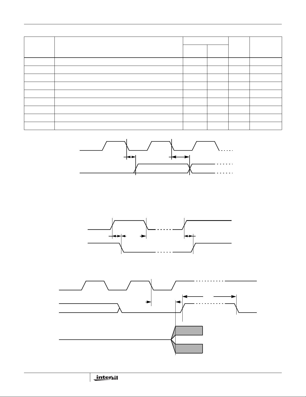
AC Electrical Specifications (Over recommended operating conditions unless otherwise stated).
LIMITS
MIN
SYMBOL PARAMETER
f
SCL
t
LOW
t
HIGH
t
R
t
F
,
(Note 11) Noise suppression time constant (glitch filter) 20 ns 10
T
i
t
SU:STA
t
HD:STA
SCL clock frequency 0 100 kHz 10
Clock LOW period 4700 ns 10
Clock HIGH period 4000 ns 10
SCL and SDA rise time 1000 ns 10
SCL and SDA fall time 300 ns 10
Start condition setup time (for a repeated start condition) 4000 ns 10 and 12
Start condition hold time 4000 ns 10 and 12
(Note 11)
MAX
(Note 11)
UNIT
REFERENCE
FIGURE
NUMBER(S)
12
FN8164.6
August 31, 2007
X9241A
www.BDTIC.com/Intersil
AC Electrical Specifications (Over recommended operating conditions unless otherwise stated). (Continued)
LIMITS
SYMBOL PARAMETER
t
SU:DAT
t
HD:DAT
t
AA
t
DH
t
SU:STO
t
BUF
t
WR
t
STPWV
t
CLWV
Data in setup time 250 ns 10
Data in hold time 0 ns 10
SCL LOW to SDA data out valid 3500 ns 11
Data out hold time 30 ns 11
Stop condition setup time 4000 ns 10 and 12
Bus free time prior to new transmission 4700 ns 10
Write cycle time (nonvolatile write operation) 10 ms 13
Wiper response time from stop generation 500 µs 13
Wiper response from SCL LOW 1000 µs 6
SCL
MIN
(Note 11)
MAX
(Note 11)
UNIT
REFERENCE
FIGURE
NUMBER(S)
SCL
SDA
SDA
SCL
SDA
(DATA IN)
SDA
SDA
OUT
t
SU:STA
CLOCK 8
IN
t
AA
(ACK) SDA
FIGURE 11. OUTPUT BUS TIMING
t
HD:STA
FIGURE 12. START STOP TIMING
CLOCK 9
t
STPWV
ACK
t
DH
OUT
STOP
SDA
STOP CONDITIONSTART CONDITION
t
SU:STO
OUT
t
WR
START
WIPER
OUTPUT
FIGURE 13. WRITE CYCLE AND WIPER RESPONSE TIMING
13
FN8164.6
August 31, 2007

X9241A
www.BDTIC.com/Intersil
Thin Shrink Small Outline Package Family (TSSOP)
0.25 CAB
C
SEATING
PLANE
N LEADS
E
0.10 C
M
E1
B
N
1
TOP VIEW
e
b
SEE DETAIL “X”
(N/2)+1
SIDE VIEW
(N/2)
0.10 CABM
AD
PIN #1 I.D.
0.20 C2XB A
N/2 LEAD TIPS
0.05
H
MDP0044
THIN SHRINK SMALL OUTLINE PACKAGE FAMILY
SYMBOL
NOTES:
1. Dimension “D” does not include mold flash, protrusions or gate
2. Dimension “E1” does not include interlead flash or protrusions.
3. Dimensions “D” and “E1” are measured at dAtum Plane H.
4. Dimensioning and tolerancing per ASME Y14.5M-1994.
MILLIMETERS
TOLERANCE14 LD 16 LD 20 LD 24 LD 28 LD
A 1.20 1.20 1.20 1.20 1.20 Max
A1 0.10 0.10 0.10 0.10 0.10 ±0.05
A2 0.90 0.90 0.90 0.90 0.90 ±0.05
b 0.25 0.25 0.25 0.25 0.25 +0.05/-0.06
c 0.15 0.15 0.15 0.15 0.15 +0.05/-0.06
D 5.00 5.00 6.50 7.80 9.70 ±0.10
E 6.40 6.40 6.40 6.40 6.40 Basic
E1 4.40 4.40 4.40 4.40 4.40 ±0.10
e 0.65 0.65 0.65 0.65 0.65 Basic
L 0.60 0.60 0.60 0.60 0.60 ±0.15
L1 1.00 1.00 1.00 1.00 1.00 Reference
Rev. F 2/07
burrs. Mold flash, protrusions or gate burrs shall not exceed
0.15mm per side.
Interlead flash and protrusions shall not exceed 0.25mm per
side.
c
A2
A
A1
END VIEW
DETAIL X
L1
GAUGE
PLANE
0.25
L
0° - 8°
14
FN8164.6
August 31, 2007

Small Outline Package Family (SO)
www.BDTIC.com/Intersil
A
D
NN
(N/2)+1
X9241A
h X 45°
PIN #1
E
C
SEATING
PLANE
0.004 C
E1
B
0.010 BM CA
I.D. MARK
1
e
0.010 BM CA
(N/2)
c
SEE DETAIL “X”
L1
H
A2
GAUGE
PLANE
A1
b
DETAIL X
L
4° ±4°
MDP0027
SMALL OUTLINE PACKAGE FAMILY (SO)
INCHES
SO16
SYMBOL
A 0.068 0.068 0.068 0.104 0.104 0.104 0.104 MAX -
A1 0.006 0.006 0.006 0.007 0.007 0.007 0.007 ±0.003 -
A2 0.057 0.057 0.057 0.092 0.092 0.092 0.092 ±0.002 -
b 0.017 0.017 0.017 0.017 0.017 0.017 0.017 ±0.003 -
c 0.009 0.009 0.009 0.011 0.011 0.011 0.011 ±0.001 -
D 0.193 0.341 0.390 0.406 0.504 0.606 0.704 ±0.004 1, 3
E 0.236 0.236 0.236 0.406 0.406 0.406 0.406 ±0.008 -
E1 0.154 0.154 0.154 0.295 0.295 0.295 0.295 ±0.004 2, 3
e 0.050 0.050 0.050 0.050 0.050 0.050 0.050 Basic -
L 0.025 0.025 0.025 0.030 0.030 0.030 0.030 ±0.009 -
L1 0.041 0.041 0.041 0.056 0.056 0.056 0.056 Basic -
h 0.013 0.013 0.013 0.020 0.020 0.020 0.020 Reference -
N 8 14 16 16 20 24 28 Reference -
NOTES:
1. Plastic or metal protrusions of 0.006” maximum per side are not included.
2. Plastic interlead protrusions of 0.010” maximum per side are not included.
3. Dimensions “D” and “E1” are measured at Datum Plane “H”.
4. Dimensioning and tolerancing per ASME Y14.5M-1994
(0.150”)
SO16 (0.300”)
(SOL-16)
SO20
(SOL-20)
SO24
(SOL-24)
SO28
(SOL-28)
TOLERANCE NOTESSO-8 SO-14
A
0.010
Rev. M 2/07
15
FN8164.6
August 31, 2007

Plastic Dual-In-Line Packages (PDIP)
www.BDTIC.com/Intersil
X9241A
SEATING
PLANE
D
A2
A
L
L
e
b
A1
NOTE 5
c
E
eA
eB
N
PIN #1
E1
INDEX
12 N/2
MDP0031
PLASTIC DUAL-IN-LINE PACKAGE
INCHES
SYMBOL
A 0.210 0.210 0.210 0.210 0.210 MAX
A1 0.015 0.015 0.015 0.015 0.015 MIN
A2 0.130 0.130 0.130 0.130 0.130 ±0.005
b 0.018 0.018 0.018 0.018 0.018 ±0.002
b2 0.060 0.060 0.060 0.060 0.060 +0.010/-0.015
c 0.010 0.010 0.010 0.010 0.010 +0.004/-0.002
D 0.375 0.750 0.750 0.890 1.020 ±0.010 1
E 0.310 0.310 0.310 0.310 0.310 +0.015/-0.010
E1 0.250 0.250 0.250 0.250 0.250 ±0.005 2
e 0.100 0.100 0.100 0.100 0.100 Basic
eA 0.300 0.300 0.300 0.300 0.300 Basic
eB 0.345 0.345 0.345 0.345 0.345 ±0.025
L 0.125 0.125 0.125 0.125 0.125 ±0.010
N 8 14 16 18 20 Reference
NOTES:
1. Plastic or metal protrusions of 0.010” maximum per side are not included.
2. Plastic interlead protrusions of 0.010” maximum per side are not included.
3. Dimensions E and eA are measured with the leads constrained perpendicular to the seating plane.
4. Dimension eB is measured with the lead tips unconstrained.
5. 8 and 16 lead packages have half end-leads as shown.
TOLERANCE NOTESPDIP8 PDIP14 PDIP16 PDIP18 PDIP20
b2
Rev. C 2/07
All Intersil U.S. products are manufactured, assembled and tested utilizing ISO9000 quality systems.
Intersil Corporation’s quality certifications can be viewed at www.intersil.com/design/quality
Intersil products are sold by description only. Intersil Corporation reserves the right to make changes in circuit design, software and/or specifications at any time without
notice. Accordingly, the reader is cautioned to verify that data sheets are current before placing orders. Information furnished by Intersil is believed to be accurate and
reliable. However, no responsibility is assumed by Intersil or its subsidiaries for its use; nor for any infringements of patents or other rights of third parties which may result
from its use. No license is granted by implic atio n or other wise u nde r any p a tent or patent rights of Intersil or its subsidiaries.
For information regarding Intersil Corporation and its products, see www.intersil.com
16
FN8164.6
August 31, 2007
 Loading...