

Page 1
®
www.BDTIC.com/Intersil
X90100
Data Sheet February 2, 2005
NV Electronically Programmable
Capacitor
The Intersil X90100 is a non-volatile electronically
programmable capacitor. The device is programmed through
a simple digital interface. After programming, the chosen
setting for the device is retained by internal EEPROM
storage whether or not DC power is maintained. There are
32 programmable capacitance values selectable, ranging
from 7.5pF to 14.5pF in 0.23pF increments, in single-ended
mode. The dielectric is highly stable, and the capacitance
exhibits a very low voltage coefficient. It has virtually no
dielectric absorbtion and has a very low temperature drift
coefficient in differential mode (<50ppm/°C).
The X90100 is programmed through three digital interface
pins, which have Schmitt triggers and pullup resistors to
secure code retention. The three pins, INC
, U/D, and CS,
are identical in operation to other Intersil chips with up/down
interface, such as the X9315 5-bit Digitally Controlled
Potentiometer (DCP).
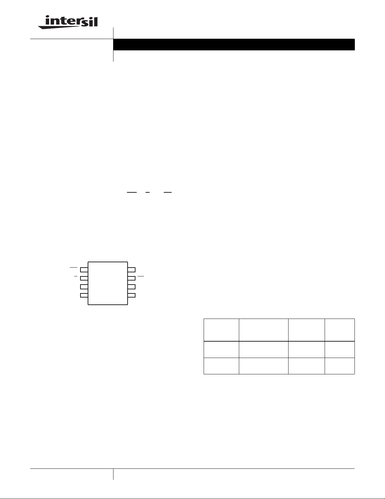
Pinout
X90100
(8 LD MSOP)
TOP VIEW
INC
U/D
Vss
Cp
1
2
3
4
V
8
CC
CS
7
N/C
6
Cm
5
FN8156.0
Features
• Non-volatile EEPROM storage of programmed trim codes
• Power On Recall of capacitance setting
• High-Performance Electronically Trimmable Capacitance
• Excellent linearity: <0.5 LSB error
• Very Simple Digital Interface
• Fast adjustments: 5µs max incremental change
• Eliminates the need for mechanical tuning
• Capacitance trimmable from 7.5pF to 14.5pF (singleended mode)
• Packages:
- MSOP (1.1mm x 3.0mm x 3.0mm)
Applications
• Post-trim of low-cost regenerative receivers
• Tunable RF stages
• Low-cost, Low temperature drift oscillators
• Garage door openers
• Keyless entry
• Industrial wireless control
• Capacitive sensor trimming
• RFID tags
Ordering Information
ORDERING
NUMBER C
X90100M8I 7.5pF to 14.5pF,
X90100M8IT1 7.5pF to 14.5pF,
1
CAUTION: These devices are sensitive to electrostatic discharge; follow proper IC Handling Procedures.
1-888-INTERSIL or 321-724-7143
| Intersil (and design) is a registered trademark of Intersil Americas Inc.
All other trademarks mentioned are the property of their respective owners.
TOTAL
Single Ended
Single Ended
Copyright Intersil Americas Inc. 2005. All Rights Reserved
PACKAGE
8 Ld MSOP -40 to +85
8 Ld MSOP
Tape and Reel
TEMP
RANGE
(°C)
-40 to +85
Page 2

Block Diagram
www.BDTIC.com/Intersil
X90100
Cm
U/D
INC
V
CC
1*C
U
2*C
4*C
8*C
16*C
2
U
U
U
U
C
PAD
Logic and E
Power On Reset
Cp
C
PAD
V
SS
CS
Pin Descriptions
MSOP SYMBOL BRIEF DESCRIPTION
1INC
2U/D
3V
4CpCp. The high (Cp) and low (Cm) terminals of the X90100 are equivalent to the fixed terminals of a mechanical
5CmCm. The high (Cp) and low (Cm) terminals of the X90100 are equivalent to the fixed terminals of a mechanical
6N/CNot Connected. Must be floating.
7CS
8V
SS
CC
Increment (INC). The INC input is negative-edge triggered. Toggling INC will move the capacitance value and
either increment or decrement the counter in the direction indicated by the logic level on the U/D
Up/Down (U/D). The U/D input controls the direction of the trimmed capacitor value and whether the counter
is incremented or decremented.
Ground.
trimmable capacitor. The minimum dc voltage is VSS and the maximum is VCC. The value of capacitance
across the terminals is determined by digital inputs INC
trimmable capacitor. The minimum dc voltage is VSS and the maximum is VCC. The value of capacitance
across the terminals is determined by digital inputs INC
Chip Select (CS). The device is selected when the CS input is LOW. The current counter value is stored in
nonvolatile memory when CS
complete the X90100 will be placed in the low power standby mode until the device is selected once again.
Positive Supply Voltage.
is returned HIGH while the INC input is also HIGH. After the store operation is
, U/D, and CS.
, U/D, and CS.
input.
2
FN8156.0
February 2, 2005
Page 3
X90100
www.BDTIC.com/Intersil
Absolute Maximum Ratings
Temperature under bias . . . . . . . . . . . . . . . . . . . . . .-65°C to +135°C
Storage temperature . . . . . . . . . . . . . . . . . . . . . . . .-65°C to +150°C
Voltage on CS
C
M
CAUTION: Stresses above those listed under “Absolute Maximum Ratings” may cause permanent damage to the device. This is a stress rating only; the functional
operation of the device (at these or any other conditions above those listed in the operational sections of this specification) is not implied. Exposure to absolute
maximum rating conditions for extended periods may affect device reliability.
, INC, U/D, CP, and
with respect to VSS. . . . . . . . . . . . . . . . . . . . . . . . -1V to +7V
∆V = |V
Lead temperature (soldering 10 seconds) . . . . . . . . . . . . . . . . 300°C
|. . . . . . . . . . . . . . . . . . . . . . . . . . . . . . . . . . . . . . . 5V
CP-VCM
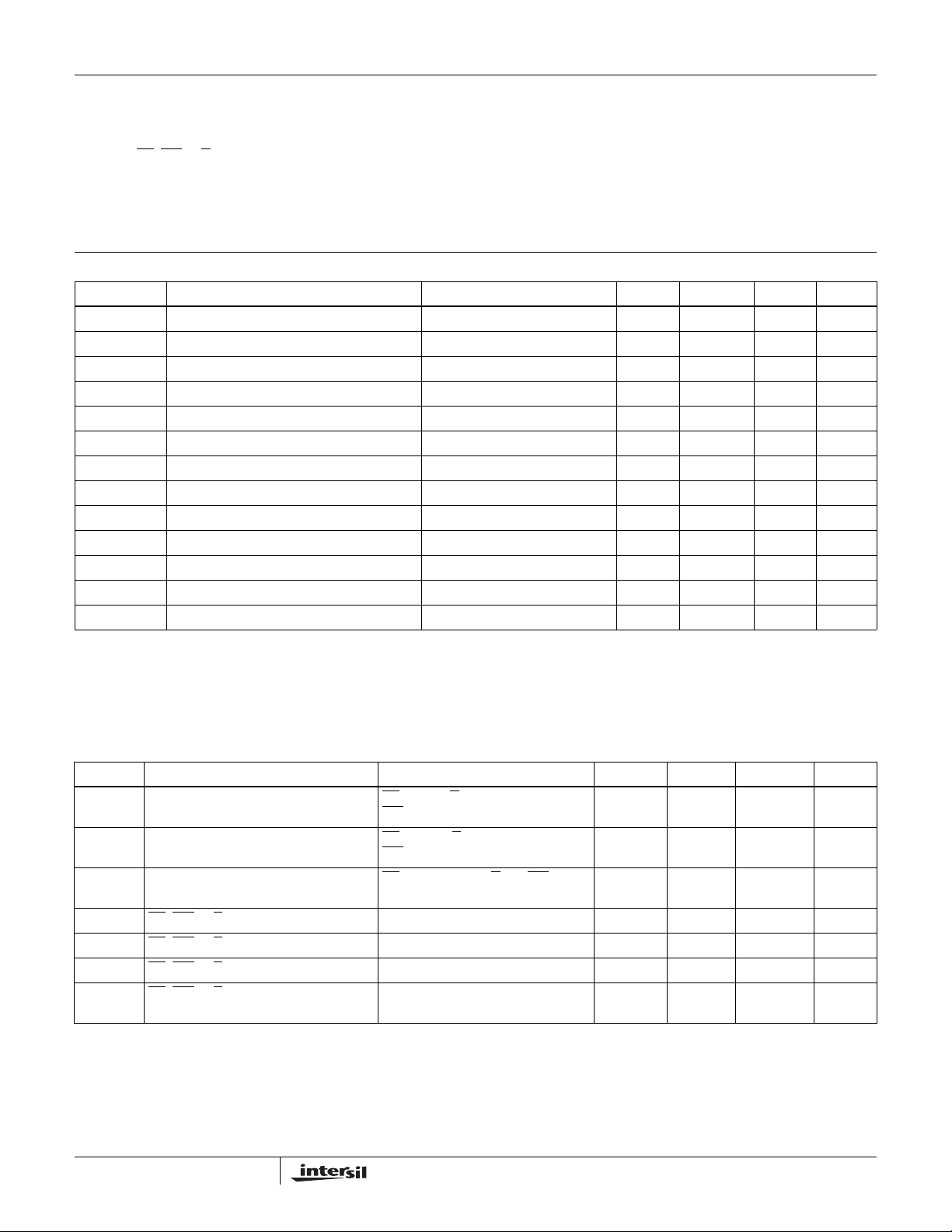
Capacitor Specifications V
SYMBOL PARAMETER TEST CONDITIONS/NOTES MIN TYP
Absolute accuracy ±15 %
V
Cp
V
Cm
∆C Capacitance increments 0.23 pF
∆C Capacitance range 7pF
C
TOTAL
C
TOTAL
Q Quality factor
INL Absolute linearity error
DNL Relative linearity error
TC
V
CC
Notes: (1) Absolute linearity is used to determine actual capacitance versus expected capacitance = C
(2) Relative linearity is a measure of the error in step size between settings = C
(3) lsb = least significant bit = C
(4) Typical v alues are f or T
(5) This parameter is not 100% tested.
Cp terminal voltage 0 V
Cm terminal voltage 0 V
Capacitance at Code=0 7.5 pF
Capacitance at Code=31 14.5 pF
(5)
Resolution 5bits
C
1
Temperature Coefficient
TOTAL
Supply Voltage 2.7 5.5 V
= +5V, TA = 25°C, single ended mode, CM = 0V, unless otherwise stated.
CC
f = 315MHz 7
(1)
(2)
(5)
/31.
TOT
= 25°C and nominal supply voltage.
A
Differential Mode ±50 ppm/°C
-[C
(n+1)
+ Ml] = ±0.15 Ml.
(n)
(actual) - C
(n)
(4)
±0.15 lsb
±0.15 lsb
(n)
MAX UNIT
CC
CC
(expected) = ±0.15 Ml.
V
V
DC Electrical Specifications V
SYMBOL PARAMETER TEST CONDITIONS MIN TYP
VCC active current (Increment) CS = VIL, U/D = VIL or VIH and
VCC active current (Store) (EEPROM
Store)
Standby supply current CS = VCC - 0.3V, U/D and INC = VSS
SB
I
CS, INC, U/D input leakage current VIN = V
LI
CS, INC, U/D input HIGH voltage V
IH
CS, INC, U/D input LOW voltage -0.5 V
IL
(5)
, INC, U/D input capacitance VCC = 5V, VIN = VSS, TA= 25°C,
CS
C
I
CC1
I
CC2
I
V
V
IN
= 5V, TA = 25°C unless otherwise specified.
CC
INC
= 0.4V @ max. t
CS = VIH, U/D = VIL or VIH and
=V
CC
@ max. t
IH
- 0.3V
SS
INC
or V
f=1MHz
CYC
WR
x 0.7 VCC + 0.5 V
CC
3
(4)
50 100 µA
250 500 µA
0.5 2 µA
-15 µA
MAX UNIT
x 0.1 V
CC
10 pF
FN8156.0
February 2, 2005
Page 4
www.BDTIC.com/Intersil
Endurance and Data Retention V
PARAMETER MIN UNIT
Minimum endurance 100,000 Data changes per bit
Data retention 100 Years
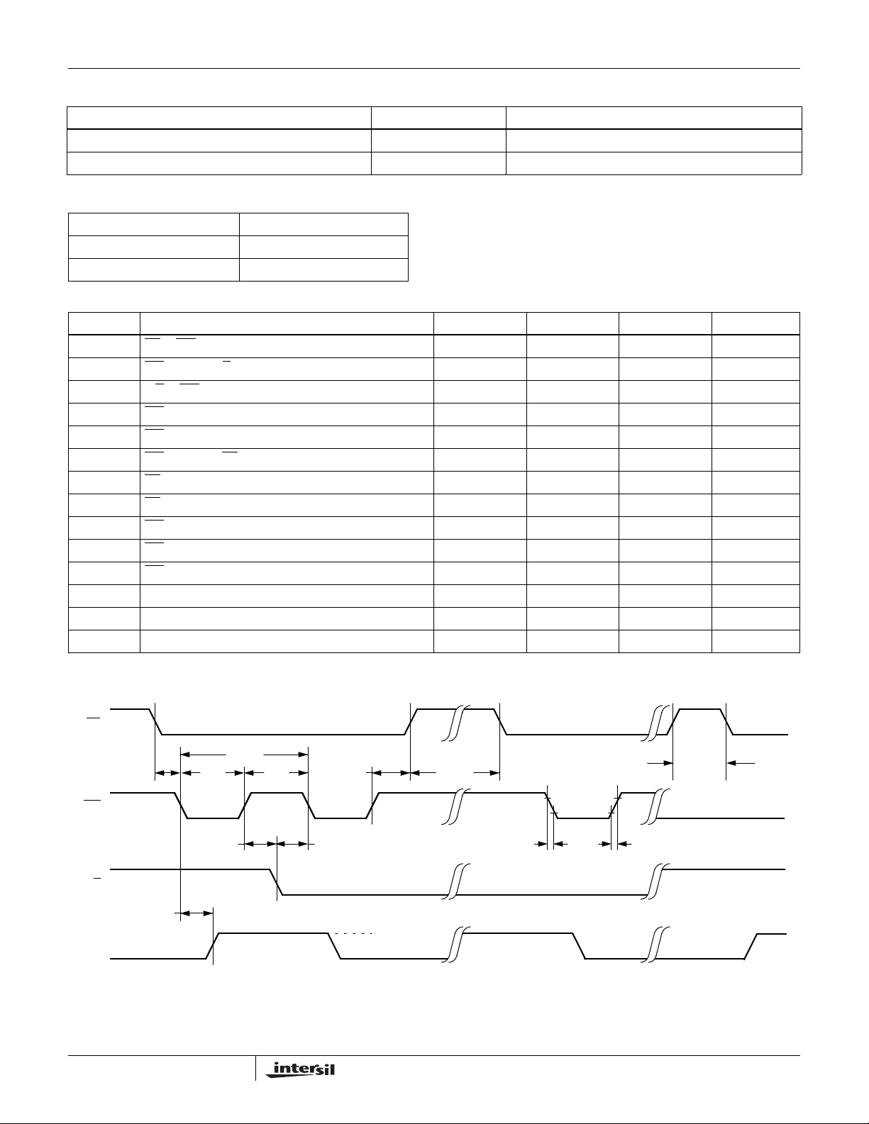
AC Conditions of Test
Input pulse levels 0V to 3V
Input rise and fall times 10ns
Input reference levels 1.5V
X90100
= 5V, TA = 25°C unless otherwise specified
CC
AC Electrical Specifications V
= 5V, TA = 25°C unless otherwise specified.
CC
SYMBOL PARAMETER MIN TYP
t
t
t
t
lL
t
lH
t
t
CPHNS
t
CPHS
t
t
CYC
t
R, tF
t
PU
t
R VCC
t
WR
DI
IW
CS to INC setup 100 ns
Cl
INC HIGH to U/D change 100 ns
lD
U/D to INC setup 100 ns
(7)
INC
LOW period 1 µs
(7)
INC
HIGH period 1 µs
INC Inactive to CS inactive 1 µs
lC
(5)
(5)
Deselect time (NO STORE) 1 µs
CS
CS
Deselect time (STORE) 10 ms
INC to C
change 1 5 µs
TOTAL
INC cycle time 4 µs
(5)
INC
input rise and fall time 500 µs
(5)
Power up to capacitance stable 5 µs
(5)
VCC power-up rate 0.2 50 V/ms
(5)
Store cycle 510ms
AC Timing
(4)
MAX UNIT
CS
t
CYC
t
IC
t
DI
(6)
MI
INC
U/D
C
TOTAL
t
CI
t
IW
t
IL
t
ID
t
IH
Notes: (6) MI in the A.C. timing diagram refers to the minimum incremental change in the C
+ tIL ≥ 4µs
(7) t
IH
(Store)
t
CPHS
t
F
TOTAL
4
t
CPHNS
90% 90%
10%
t
R
output due to a change in the counter value.
February 2, 2005
FN8156.0
Page 5
X90100
www.BDTIC.com/Intersil
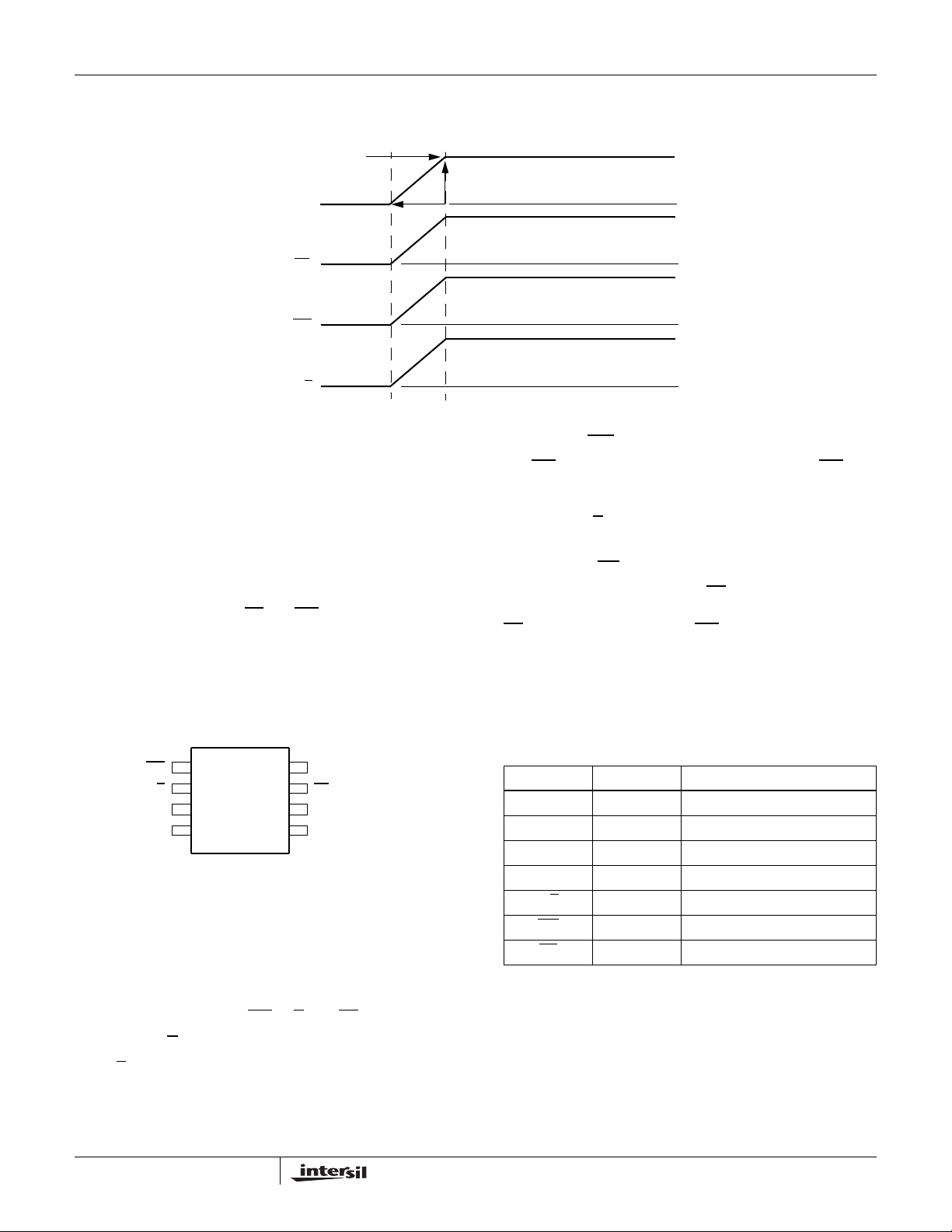
Power Up Timing (Digital Inputs Floating, Internal Pullup Action Shown)
VCC = 3.3 or 5.0V
tRV
V
CC
CS
INC
U/D
CC
Power Up and Down Requirements
There are no restrictions on the power-up or power-down
conditions of V
pins provided that V
to V
, VCm, i.e., VCC ≥ VCp, VCm. The VCC ramp rate spec
Cp
and the voltages applied to the Cp, Cm
CC
is always more positive than or equal
CC
is always in effect.
Powerup Requirements
In order to prevent unwanted tap position changes or an
inadvertant store, bring the CS
concurrently with the V
CC
active pullups to provide reliable powerup operation. See
powerup timing diagram.
and INC high before or
pin. The logic inputs have internal
Pin Configuration
MSOP
INC
U/D
Vss
Cp
1
2
X90100
3
4
V
8
CC
CS
7
N/C (leave floating)
6
Cm
5
Detailed Pin Descriptions
Cp and Cm
The high (Cp) and low (Cm) terminals of the X90100 are
equivalent to the fixed terminals of a mechanical trimmable
capacitor. The minimum dc voltage is V
is V
. The value of capacitance across the terminals is
CC
determined by digital inputs INC
, U/D, and CS.
Up/Down (U/D)
The U/D input controls the direction of the trimmed capacitor
value and whether the counter is incremented or
decremented. This pin has an active current source pullup.
and the maximum
SS
Increment (INC)
The INC input is negative-edge triggered. Toggling INC will
move the capacitance value and either increment or
decrement the counter in the direction indicated by the logic
level on the U/D
input. This pin has an active current source
pullup.
Chip Select (CS)
The device is selected when the CS input is LOW. The
current counter value is stored in nonvolatile memory when
CS
is returned HIGH while the INC input is also HIGH. After
the store operation is complete the X90100 will be placed in
the low power standby mode until the device is selected
once again. This pin has active circuit source pullup.
N/C - This pin should be left floating.
Pin Names
SYMBOL DEFAULT DESCRIPTION
Cp output Positive capacitor terminal
Cm output Negative capacitor terminal
V
V
U/D
INC
CS
SS
CC
supply Ground
supply Positive supply voltage
pull up Up/Down control input
pull up Increment control input
pull up Chip Select control input
Principles of Operation
There are three sections of the X90100: the input control,
counter and decode section; the nonvolatile memory; and
the capacitor array. The input control section operates just
like an up/down counter. The output of this counter is
decoded to turn on electronic switches connecting internal
units to the sum capacitor. Under the proper conditions the
contents of the counter can be stored in nonvolatile memory
5
FN8156.0
February 2, 2005
Page 6

X90100
www.BDTIC.com/Intersil
and retained for future use. The capacitor array is comprised
of 31 individual capacitors connected in parallel. At one end
of each element is an electronic switch that connects it to the
sum.
The capacitor, when at either end of the range, acts like its
mechanical equivalent and does not move beyond the last
position. That is, the counter does not wrap around when
clocked to either extreme.
The electronic switches on the device operate in a “make
before break” mode when the counter changes positions. If
the counter is moved several positions, multiple units are
connected to the total for t
C
value for the device can temporarily be increased by
TOTAL
(INC to C
IW
TOTAL
change). The
a significant amount if the counter is moved several
positions.
When the device is powered-down, the last counter position
stored will be maintained in the nonvolatile memory. When
power is restored, the contents of the memory are recalled
and the capacitor is set to the value last stored.
Instructions and Programming
The INC, U/D and CS inputs control the movement of the
capacitor total value. With CS
selected and enabled to respond to the U/D
HIGH to LOW transitions on INC
(depending on the state of the U/D
The output of this counter is decoded to select one of thirty
two capacitor combinations for the capacitor array.
The value of the counter is stored in nonvolatile memory
whenever CS
transitions HIGH while the INC input is also
HIGH.
set LOW the device is
and INC inputs.
will increment or decrement
input) a five bit counter.
The system may select the X90100, move the capacitor
value and deselect the device without having to store the
latest count total in nonvolatile memory. After the count
movement is performed as described above and once the
new position is reached, the system must keep INC
while taking CS
HIGH. The new C
TOTAL
value will be
LOW
maintained until changed by the system or until a powerup/down cycle recalled the previously stored data.
This procedure allows the system to always power-up to a
preset value stored in nonvolatile memory; then during
system operation minor adjustments can be made. The
adjustments might be based on user preference, system
parameter changes due to temperature drift, etc.
The state of U/D
may be changed while CS remains LOW.
This allows the host system to enable the device and then
move the counter up and down until the proper trim is
attained.
Mode Selection
CS INC U/D MODE
L H Cap Value Up
L L Cap Value Down
H X Store Cap Position
H X X Standby Current
L X No Store, Return To Standby
L H Cap Value Up (not recommended)
L L Cap Value Down (not recommended)
Table of Values
X90100
Example of a single-ended circuit Example of a differential mode circuit
C
OUT
Differential Mode
Code
=
• 0.35 + 1.00 (pF)
0 ≤ Code ≤ 31
C
m
C
p
X90100
C
p
C
s
Oscillator
Circuit
FN8156.0
February 2, 2005
Single-Ended Mode
OUT
=
Code
• 7.0 + 7.5 (pF)
31
0 ≤ Code ≤ 31
X1
Oscillator
Circuit
X2
C
C
p
C
m
6
Page 7
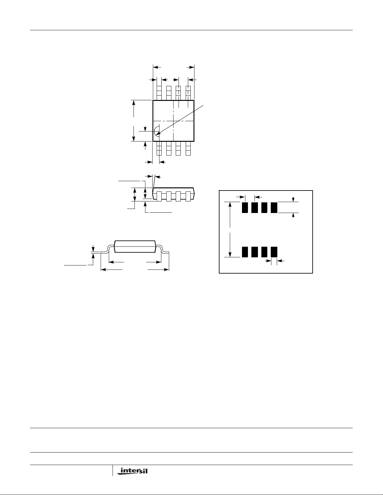
Packaging Information
www.BDTIC.com/Intersil
8-Lead Miniature Small Outline Gull Wing Package Type M
0.012 + 0.006 / -0.002
(0.30 + 0.15 / -0.05)
0.118 ± 0.002
(3.00 ± 0.05)
0.030 (0.76)
X90100
0.118 ± 0.002
(3.00 ± 0.05)
0.0216 (0.55)
0.0256 (0.65) Typ.
R 0.014 (0.36)
0.007 (0.18)
0.005 (0.13)
0.036 (0.91)
0.032 (0.81)
0.040 ± 0.002
(1.02 ± 0.05)
7° Typ.
0.008 (0.20)
0.004 (0.10)
0.150 (3.81)
Ref.
0.193 (4.90)
Ref.
NOTE:
1. ALL DIMENSIONS IN INCHES AND (MILLIMETERS)
0.220"
FOOTPRINT
0.0256" Typical
0.025"
Typical
0.020"
Typical
8 Places
All Intersil U.S. products are manufactured, assembled and tested utilizing ISO9000 quality systems.
Intersil Corporation’s quality certifications can be viewed at www.intersil.com/design/quality
Intersil products are sold by description only. Intersil Corporation reserves the right to make changes in circuit design, software and/or specifications at any time without
notice. Accordingly, the reader is cautioned to verify that data sheets are current before placing orders. Information furnished by Intersil is believed to be accurate and
reliable. However, no responsibility is assumed by Intersil or its subsidiaries for its use; nor for any infringements of patents or other rights of third parties which may result
from its use. No license is granted by implication or otherwise under any patent or patent rights of Intersil or its subsidiaries.
For information regarding Intersil Corporation and its products, see www.intersil.com
7
FN8156.0
February 2, 2005
 Loading...