intersil X80000, X80001 DATA SHEET

查询X80000供应商
®
X80000, X80001
Data Sheet March 18, 2005
Smart Power Plug™ Penta-Power
Sequence Controller with Hot Swap
The X80000 contains three major functions: a power
communications controller, a power sequencing controller,
and a hotswap controller.
The power communications controller allows smart power
supply control via the backplane using the SMBus protocol.
The system can check for voltage, current, and
manufacturing ID compliance before board insertion. The
power distribution network can monitor the status of the
negative voltage supply, DC voltage supplies, and hardshort
events by accessing the Fault Detection Register and
General Purpose EEPROM of the device. Each device has a
unique slave address for identification.
The power sequencer controller time sequences up to five
DC-DC modules. The X80000 allows for various hardwired
configurations, either parallel or relay sequencing modes.
The power good, enable and voltage good signals provide
for flexible DC-DC timing configurations. Each voltage
enable signal has a programmable delay. In addition, the
voltage good signals can be monitored remotely via the fault
detection register (thru the SMBus).
The hot swap controller allows a board to be safely inserted
and removed from a live backplane without turning off the
main power supply. The X80000 family of devices offers a
modular, power distribution approach by providing flexibility
to solve the hotswap and power sequencing issues for
insertion, operations, and extraction. Hardshort Detection
and Retry with Delay, Noise filtering, Insertion Overcurrent
Bypass, and Gate Current selection are some of the
programmable features of the device.
During insertion, the gate of an external power MOSFET is
clamped low to suppress contact bounce. The
undervoltage/overvoltage circuits and the power on reset
circuitry suppress the gate turn on until the mechanical
bounce has ended. The X80000 turns on the gate with a
user set slew rate to limit the inrush current and incorporates
an electronic circuit breaker set by a sense resistor. After the
load is successfully charged, the PWRGD signal is asserted;
indicating that the device is ready to power sequence the
DC-DC power bricks.
FN8148.0
Features
• Integrates Three Major Functions
- Smart Power Plug communications
- Programmable power sequencing
- Programmable Hot Swap controller
• Smart Power Plug™
- Intelligent board insertion allows verification of board
and power supply resources prior to system insertion.
- Fault detection register records the cause of the faults
- Soft extraction
- Soft re-insertion
- Remote gate shutdown/turn on
- Power ID/manufacturing ID memory (2kb of EEPROM)
• Programmable Power Sequencing
- Sequence up to 5 DC/DC converters.
- Four independent voltage enable pins
- Four programmable time delay circuits
- Soft Power Sequencing - restart sequence without
power cycling.
• Hot Swap Controller
- Programmable overvoltage and undervoltage protection
- Undervoltage lockout for battery/redundant supplies
- Programmable slew rate for external FET gate control
- Electronic circuit breaker - overcurrent detection and
gate shut-off
- Programmable overcurrent limit during Insertion
- Programmable hardshort retry with retry failure flag
- Typically operates from -30V to -80V. Tolerates
transients to -200V (limited by external components)
• Available Packages
- 32-lead Quad No-Lead Frame (QFN)
Applications
• -48V Hot Swap Power Backplane/Distribution Central
Office, Ethernet for VOIP
• Card Insertion Detection
• Power Sequencing DC-DC/Power Bricks
• IP Phone Applications
• Databus Power Interfacing
• Custom Industrial Power Backplanes
• Distributed Power Systems
1
CAUTION: These devices are sensitive to electrostatic discharge; follow proper IC Handling Procedures.
1-888-INTERSIL or 321-724-7143
| Intersil (and design) is a registered trademark of Intersil Americas Inc.
All other trademarks mentioned are the property of their respective owners.
Copyright Intersil Americas Inc. 2005. All Rights Reserved
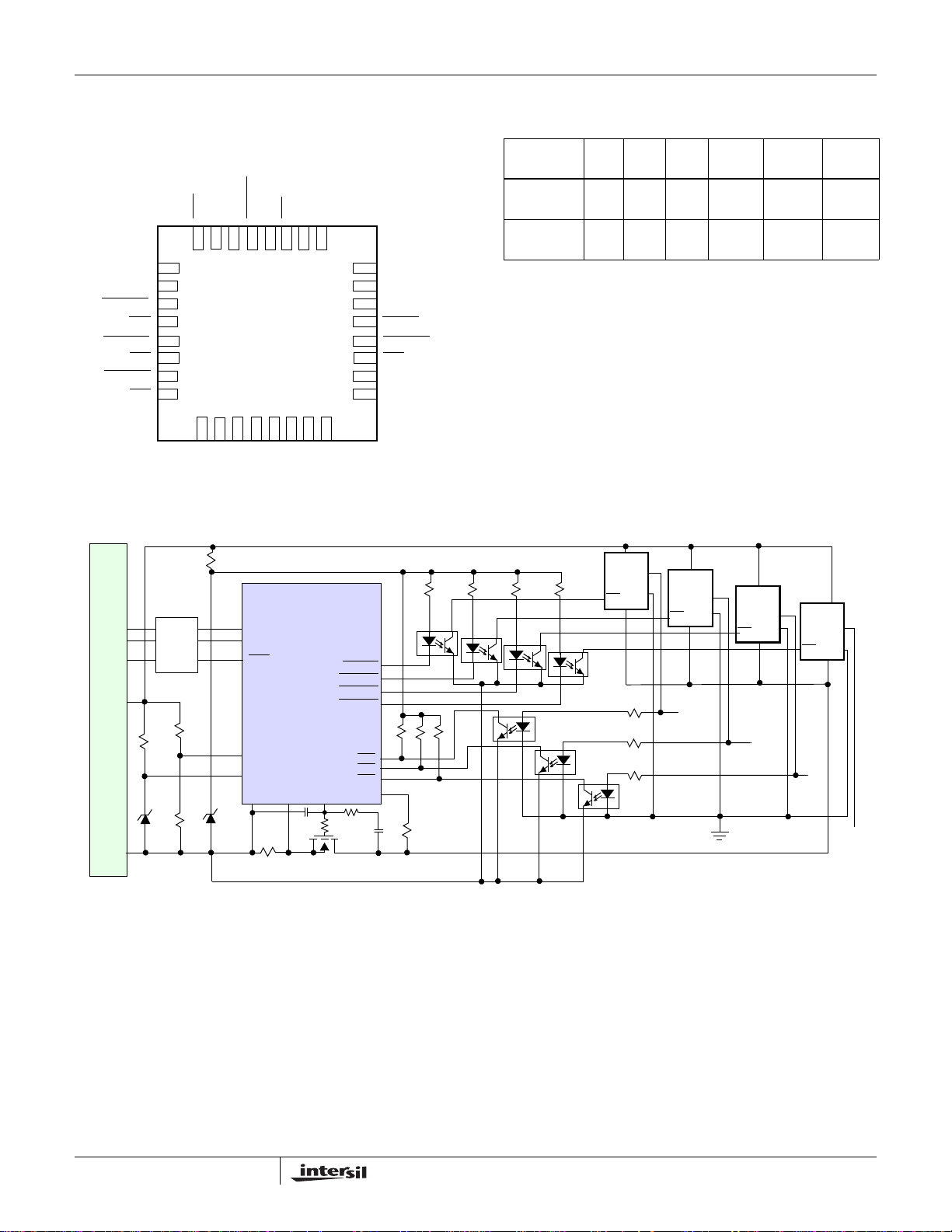
Pinout
V4GOOD
V3GOOD
V2GOOD
V
RGO
A0
EN4
EN3
EN2
X80000, X80001
X80000, X80001
(7X7 QFN)
TOP VIEW
GQ0
GQ1
PWRGD
I
MRH
32
1
BATT-ON
I
2
3
4
(7mm x 7mm)
5
6
7
817
910111213 14
EE
FAR
NC
V
262728293031
25
NC
24
MRC
23
WP
22
RESET
21
20
V1GOOD
EN1
19
SCL
18
SDA
15
16
Ordering Information
PAR T
NUMBER OV UV1 UV2
X80000Q32I 74.9 42.4 33.2 I 32 Ld
X80001Q32I 68.0 42.4 33.2 I 32 Ld
TEMP
RANGE PKG
QFN
QFN
PART
MARK
80000I
80001I
EE
DD
V
V
Typical Application
BackPlane
SCL
SDA
Insert
Control
-48V
RTN
-48V
Opto-
Isolation
R5
30K
1%
12V
R4
182K
1%
R6
10K
1%
4.7V
V
UV/OV
V
V
SCL
SDA
MRH
UV/OV
DD
V
EE
0.02Ω
SENSE
Rs
5%
GATE
OV=71V
UV=37V
SENSE
NC
DRAIN
X80000
X80001
GATE
0.1µF
IRFR120
Q1
A1
PWRGD
V1GOOD
V2GOOD
V3GOOD
DRAIN
100
EN1
EN2
EN3
4.7K
3.3n
100K
DC-DC
Module
1
ON/OFF
DC-DC
Module
2
ON/OFF
V1
DC-DC
Module
3
ON/OFF
V2
DC-DC
Module
4
ON/OFF
V3
V4
2
FN8148.0
March 18, 2005

X80000, X80001
Absolute Maximum Ratings Recommended Operating Conditions
Temperature under bias . . . . . . . . . . . . . . . . . . . . . –65°C to +135°C
Storage temperature . . . . . . . . . . . . . . . . . . . . . . . –65°C to +150°C
Voltage on given pin (Hot Side Functions):
V
ov/uv pin
SENSE pin . . . . . . . . . . . . . . . . . . . . . . . . . . . . . . . . 400mV + V
VEE pin. . . . . . . . . . . . . . . . . . . . . . . . . . . . . . . . . . . . . . . . . . -80V
DRAIN pin . . . . . . . . . . . . . . . . . . . . . . . . . . . . . . . . . . 48V + V
PWRGD pin . . . . . . . . . . . . . . . . . . . . . . . . . . . . . . . . . . 7V + V
GATE pin . . . . . . . . . . . . . . . . . . . . . . . . . . . . . . . . . . . VDD + V
FAR pin . . . . . . . . . . . . . . . . . . . . . . . . . . . . . . . . . . . . . 7V + V
MRH pin . . . . . . . . . . . . . . . . . . . . . . . . . . . . . . . . . . . . 5.5V + V
BATT_ON pin. . . . . . . . . . . . . . . . . . . . . . . . . . . . . . . .5.5V + V
. . . . . . . . . . . . . . . . . . . . . . . . . . . . . . . . . . . 5.5V + V
EE
EE
EE
EE
EE
EE
EE
EE
Voltage on given pin (Cold Side Functions):
ENi
pins (i = 1 to 4) . . . . . . . . . . . . . . . . . . . . . . . . . . . . . . . . . .5V
ViGOOD
RESET pin . . . . . . . . . . . . . . . . . . . . . . . . . . . . . . . . . .5.5V + V
SDA, SCL, WP, A0, A1 pins . . . . . . . . . . . . . . . . . . . . . 5.5V + V
MRC pin . . . . . . . . . . . . . . . . . . . . . . . . . . . . . . . . . . . . 5.5V + V
IGQ1 and IGQ0 pins . . . . . . . . . . . . . . . . . . . . . . . . . .5.5V + V
VDD pin . . . . . . . . . . . . . . . . . . . . . . . . . . . . . . . . . . . . 14V + V
D.C. output current. . . . . . . . . . . . . . . . . . . . . . . . . . . . . . . . . . . 5mA
pins (i = 1 to 4) . . . . . . . . . . . . . . . . . . . . . . .5.5V + V
EE
EE
EE
EE
EE
EE
Lead temperature (soldering, 10 seconds) . . . . . . . . . . . . . . .300°C
CAUTION: Stresses above those listed under “Absolute Maximum Ratings” may cause permanent damage to the device. This is a stress rating only; functional
operation of the device (at these or any other conditions above those listed in the operational sections of this specification) is not implied. Exposure to absolute maximum
rating conditions for extended periods may affect device reliability.
Temperature Range (Industrial) . . . . . . . . . . . . . . . . . . -40°C to 85°C
Supply Voltage (V
) . . . . . . . . . . . . . . . . . . . . . . . . . . . . . . . . .12V
DD
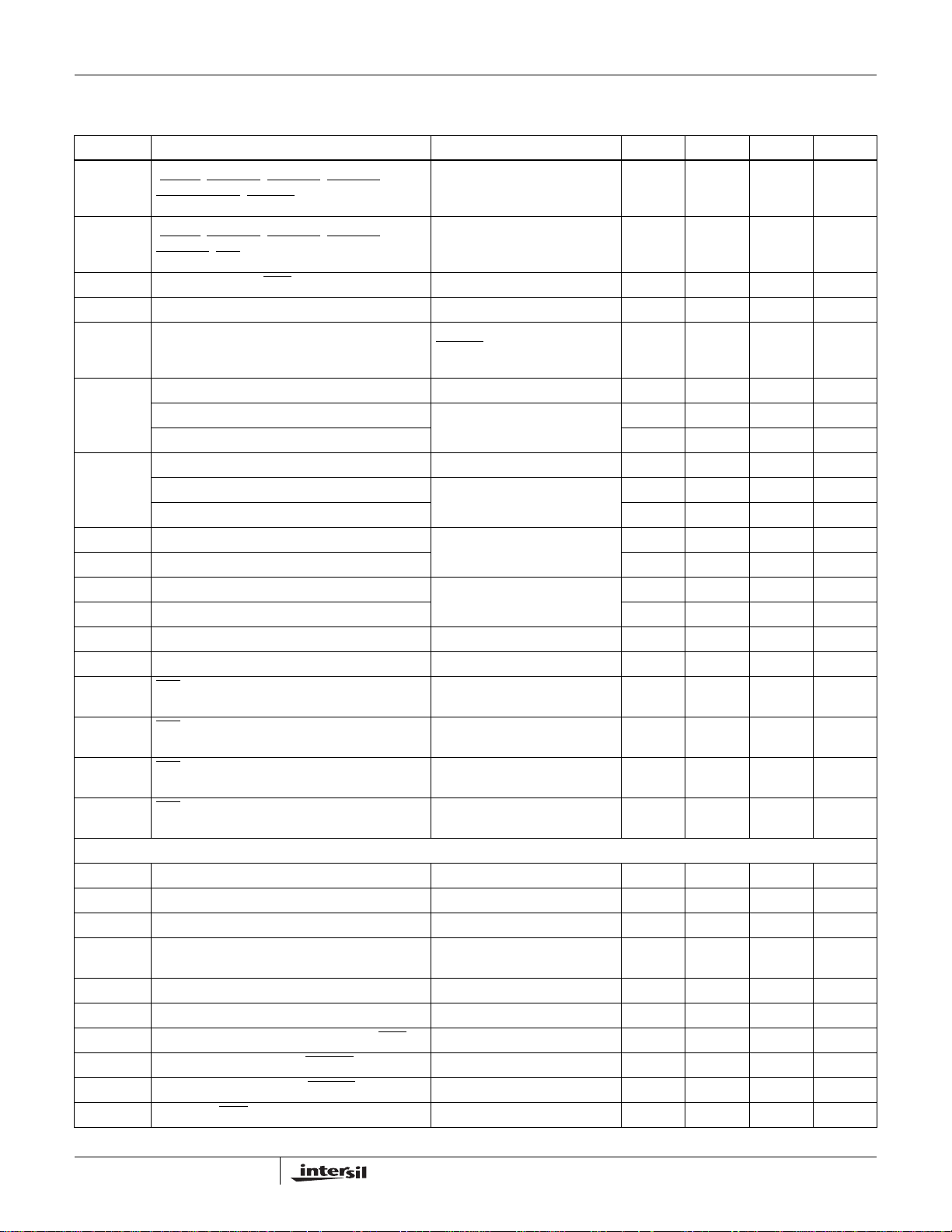
Electrical Specifications Standard Settings
Over the recommended operating conditions unless otherwise specified.
SYMBOL PARAMETER TEST CONDITIONS MIN TYP MAX UNIT
DC CHARACTERISTICS
V
I
DD
V
RGO
I
RGO
I
GATE
V
GATE
V
PGA
V
V
I
I
LO
V
V
DD
IHB
ILB
Supply Operating Range 10 12 14 V
Supply Current 2.5 5 mA
Regulated 5V output I
V
current output 50 µA
RGO
Gate Pin Current Gate Drive On,
External Gate Drive (Slew Rate Control) I
Power Good Threshold (PWRGD High to Low) Referenced to V
= 10µA 4.5 5.5
RGO
46.2 52.5 58.8 µA
V
= VEE,
GATE
V
= V
SENSE
- VEE = 3V
V
GATE
V
SENSE-VEE
= 50µA VDD-0.01 V
GATE
V
< V
UV1
(sourcing)
EE
= 0.1V (sinking)
EE
< V
UV/OV
0.9 1 1.1 V
OV
9mA
Voltage Input High (BATT_ON) VEE + 4 VEE + 5 V
Voltage Input Low (BATT_ON) VEE + 2 V
Input Leakage Current (MRH, MRC) VIL = GND to V
LI
Output Leakage Current
(V1GOOD
RESET
Input LOW Voltage (MRH, MRC, IGQ0, IGQ1) -0.5 +
IL
Input HIGH Voltage (MRH, MRC, IGQ0, IGQ1) (VEE + 5)
IH
, V2GOOD, V3GOOD, V4GOOD,
)
All ENi
= V
CC
for i = 1 to 4 10 µA
RGO
V
EE
x 0.7
DD
10 µA
(VEE + 5)
x 0.3
+ 5)
(V
EE
+ 0.5
V
V
V
3
FN8148.0
March 18, 2005
X80000, X80001
Electrical Specifications Standard Settings
Over the recommended operating conditions unless otherwise specified. (Continued)
SYMBOL PARAMETER TEST CONDITIONS MIN TYP MAX UNIT
V
C
OUT
(Note 1)
(Note 1) Input Capacitance (MRH, MRC) VIN = 0V 6 pF
C
IN
V
OC
V
OCI
V
OVR
Output LOW Voltage
OL
(RESET
, V1GOOD, V2GOOD, V3GOOD,
V4GOOD, FAR
, PWRGD)
Output Capacitance
(RESET, V1GOOD, V2GOOD, V3GOOD,
V4GOOD
, FAR)
Overcurrent threshold VOC = V
Overcurrent threshold (Insertion) VOC = V
Overvoltage threshold (rising)
X80000 Referenced to V
X80001 3.49 3.54 3.59 V
V
OVF
Overvoltage threshold (falling)
X80000 Referenced to V
X80001 3.46 3.51 3.56 V
V
UV1R
V
UV1F
V
UV2R
V
UV2F
V
DRAINF
V
DRAINR
V
TRIP1
(Note 1)
V
TRIP2
(Note 1)
V
TRIP3
Undervoltage 1 threshold (rising) Referenced to V
Undervoltage 1 threshold (falling) 2.16 2.21 2.26 V
Undervoltage 2 threshold (rising) Referenced to V
Undervoltage 2 threshold (falling) 1.68 1.73 1.78 V
Drain sense voltage threshold (falling) Referenced to V
Drain sense voltage threshold (rising) Referenced to V
Trip Point Voltage Referenced to V
EN1
Trip Point Voltage Referenced to V
EN2
Trip Point Voltage Referenced to V
EN3
(Note 1)
V
TRIP4
(Note 1)
Trip Point Voltage Referenced to V
EN4
AC CHARACTERISTICS
t
FOC
t
FUV
t
FOV
t
VFR
t
BATT_ON
t
MRC
t
MRH
t
MRCE
t
MRCD
t
MRHE
Sense High to Gate Low 1.5 2.5 3.5 µs
Under Voltage conditions to Gate Low 0.5 1 1.5 µs
Overvoltage Conditions to Gate Low 1.0 1.5 2 µs
Overvoltage/undervoltage failure recovery time to
Gate =1V.
Delay BATT_ON Valid 100 ns
Minimum time high for reset valid on the MRC pin 5 µs
Minimum time high for reset valid on the MRH pin 5 µs
Delay from MRC enable to PWRGD HIGH No Load 1.0 1.6 µs
Delay from MRC disable to PWRGD LOW Gate is On, No Load 200 400 ns
Delay from MRH enable to Gate Pin LOW I
I
= 4.0mA VEE + 0.4 V
OL
V
= 0V 8 pF
OUT
SENSE
SENSE
- V
- V
EE
EE
45 50 55 mV
135 150 165 mV
PWRGD = HIGH
Initial Power Up condition
EE
EE
BATT-ON = V
BATT-ON = V
EE
EE
EE
RGO
EE
EE
EE
EE
EE
EE
VDD does not drop below 3V, No
3.85 3.90 3.95 V
3.82 3.87 3.92 V
2.19 2.24 2.29 V
1.71 1.76 1.81 V
0.9 1 1.1 V
1.2 1.3 1.4 V
V
÷ 2 V
RGO
1.2 1.6 2 µs
other failure conditions.
= 60µA, No Load 1.0 1.6 2.4 µs
GATE
V
V
V
4
FN8148.0
March 18, 2005
X80000, X80001
Electrical Specifications Standard Settings
Over the recommended operating conditions unless otherwise specified. (Continued)
SYMBOL PARAMETER TEST CONDITIONS MIN TYP MAX UNIT
t
MRHD
t
RESET_E
t
QC
t
SC_RETRY
t
NF
t
DPOR
t
SPOR
t
TO
t
PDHLPG
(Note 1)
t
PDLHPG
(Note 1)
t
PGHLPG
(Note 1)
t
PGLHPG
(Note 1)
NOTE:
1. This parameter is based on characterization data.
Delay from MRH disable to GATE reaching 1V I
Delay from PWRGD or ViGOOD to RESET valid
= 60µA, No Load 1.8 2.6 µs
GATE
1 µs
LOW
Delay from IGQ1 and IGQ0 to valid Gate pin
1 µs
current
Delay between retries TSC1 = 0; TSC0 = 0 90 100 110 ms
Noise Filter for Overcurrent TF1 = 0; TF0 = 1 4.5 5 5.5 µs
Device Delay before Gate assertion 45 50 55 ms
Delay after PWRGD and all ViGOOD signals are
active before RESET
assertion
TPOR1 = 0; TPOR0 = 0 90 100 110 ms
ViGOOD turn off time 50 ns
Delay from Drain good to PWRGD
Delay from Drain fail to PWRGD
Delay from Gate good to PWRGD
Delay from Gate fail to PWRGD
HIGH Drain = V
LOW Gate = V
HIGH Gate = V
LOW Drain = V
DD
DD
EE
EE
1 µs
1 µs
1 µs
1 µs
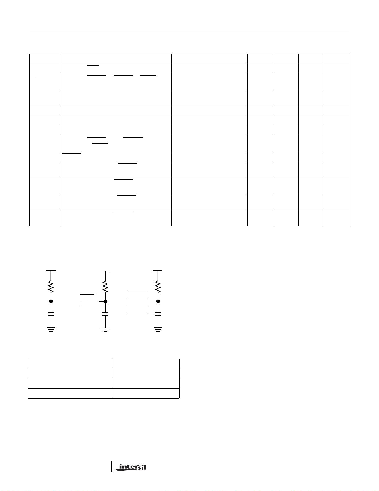
Equivalent A.C. Output Load Circuit
5V
,
,
SDA
5V
4.6kΩ
30pF
RESET
FAR
PWRGD
5V
4.6kΩ
30pF
V1GOOD,
V2GOOD,
V3GOOD
V4GOOD
A.C. Test Conditions
Input pulse levels VCC x 0.1 to VCC x 0.9
Input rise and fall times 10ns
Input and output timing levels V
Output load Standard output load
CC
x 0.5
4.6kΩ
30pF
5
FN8148.0
March 18, 2005
V
UV/OV
VDD
X80000, X80001
V
TH
t
DPOR
V
OV
V
UV
t
FOV
t
VFR
t
FUV
t
VFR
MRH
SENSE
GATE
VDD
SENSE
GATE
V
OCI
V
OC
1V 1V
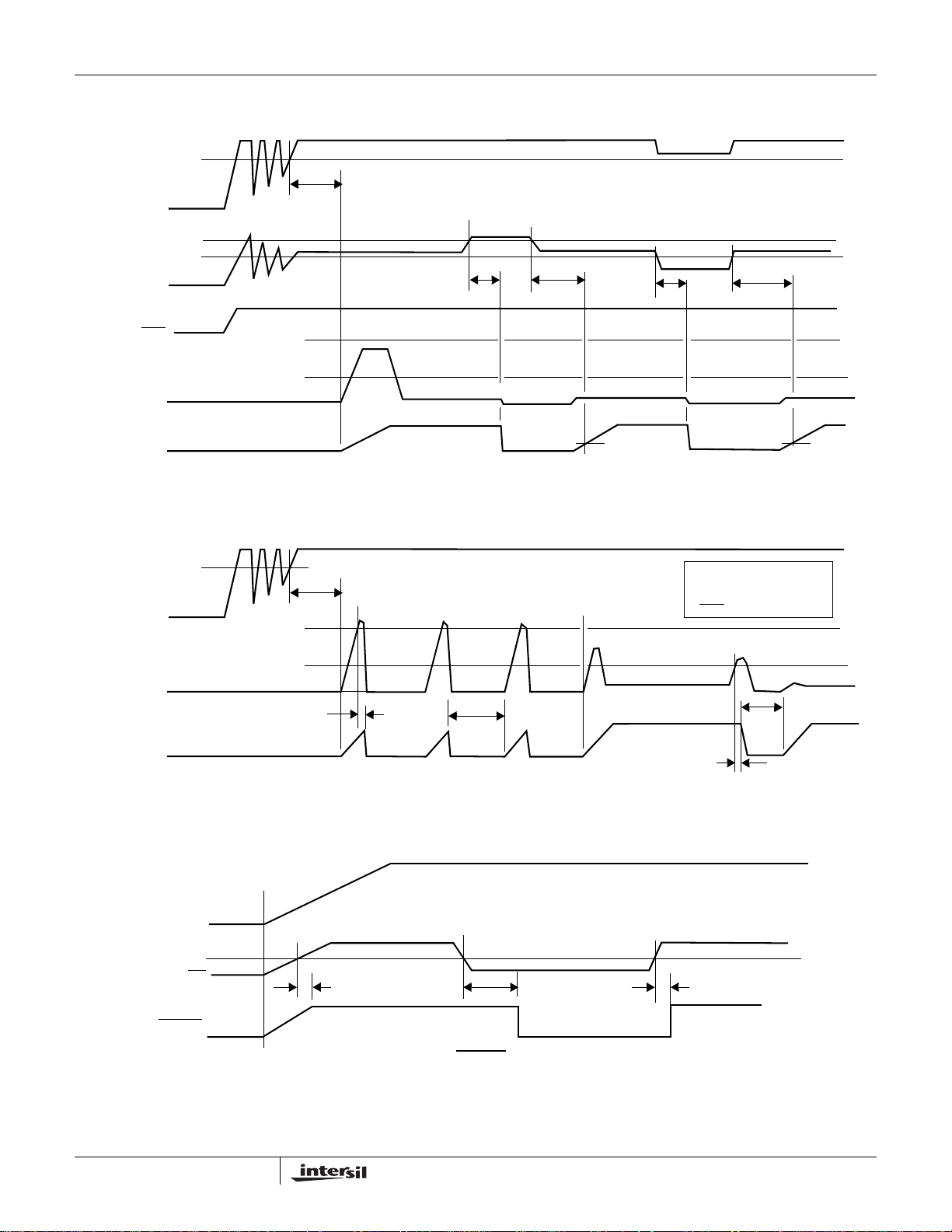
FIGURE 1. OVERVOLTAGE/UNDERVOLTAGE GATE TIMING
V
TH
t
DPOR
V
OCI
V
OC
t
FOC
t
SC_RETRY
Always Retry
V
< V
UV
MRH = HIGH
t
FOC
UV/OV
< V
OV
t
SC_RETRY
VDD
V
TRIPi
ENi
ViGOOD
Initial
Power-up
6
FIGURE 2. OVERCURRENT GATE TIMING
t
TO
t
DELAYi
Enable DC/DC supply
FIGURE 3. ViGOOD TIMINGS
t
TO
i = 1, 2, 3, 4
FN8148.0
March 18, 2005

MRH
t
MRH
X80000, X80001
MRC
t
MRC
GATE
t
MRHE
FIGURE 4. MANUAL RESET (HOT SIDE) MRH
V
DRAIN
V
GATE
PWRGD
ENi
V1GOOD
V2GOOD
t
DHLPG
t
GLHPG
1V
t
MRHD
t
DELAY1
t
DELAY2
PWRGD
t
MRCE
FIGURE 5. MANUAL RESET (COLD SIDE) MRC
t
DLHPG
t
GHLPG
t
MRCD
V3GOOD
V4GOOD
RESET
t
DELAY3
t
DELAY4
t
SPOR
PWRGD or
any ENi
(1st occurance)
FIGURE 6. PWRGD AND RESET TIMINGS
LOW to HIGH
t
RESET_E
7
FN8148.0
March 18, 2005
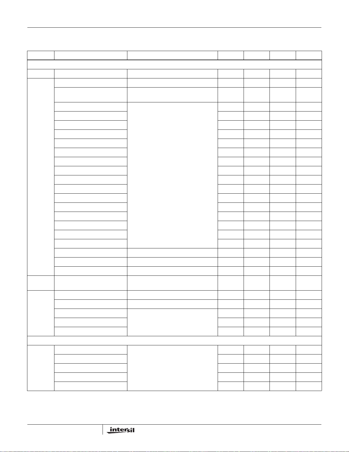
X80000, X80001
Electrical Specifications Programmable Parameters
Over the recommended operating conditions unless otherwise specified.
SYMBOL PARAMETER TEST CONDITIONS MIN. TYP. MAX. UNIT
DC CHARACTERISTICS
VCB Over Current Trip Voltage Range Factory Setting is 50mV (see VOCI). 30 100 mV
I
GATE
V
PGA
V
OCI
AC CHARACTERISTICS
t
SC_RETRY
(VCB = V
Gate Pin Pull-Up Current. (error)
(current)
- VEE) For other options, contact Intersil. -12 12 %
SENSE
Gate Drive On; V
= VEE, IGQ1=0;
GATE
IGQ0=0
IG3 = 0; IG2= 0; IG1 = 0; IG0 = 0 Factory Default 9.2 10.5 11.8 µA
IG3 = 0; IG2= 0; IG1 = 0; IG0 = 1 21.0 µA
IG3 = 0; IG2= 0; IG1 = 1; IG0 = 0 31.5 µA
IG3 = 0; IG2= 0; IG1 = 1; IG0 = 1 42.0 µA
IG3 = 0; IG2= 1; IG1 = 0; IG0 = 0 46.2 52.5 58.5 µA
IG3 = 0; IG2= 1; IG1 = 0; IG0 = 1 63.0 µA
IG3 = 0; IG2= 1; IG1 = 1; IG0 = 0 64.7 73.5 82.3 µA
IG3 = 0; IG2= 1; IG1 = 1; IG0 = 1 84.0 µA
IG3 = 1; IG2= 0; IG1 = 0; IG0 = 0 94.5 µA
IG3 = 1; IG2= 0; IG1 = 0; IG0 = 1 105.0 µA
IG3 = 1; IG2= 0; IG1 = 1; IG0 = 0 115.5 µA
IG3 = 1; IG2= 0; IG1 = 1; IG0 = 1 126.0 µA
IG3 = 1; IG2= 1; IG1 = 0; IG0 = 0 136.5 µA
IG3 = 1; IG2= 1; IG1 = 0; IG0 = 1 147.0 µA
IG3 = 1; IG2= 1; IG1 = 1; IG0 = 0 138.6 157.5 176.4 µA
IG3 = 1; IG2= 1; IG1 = 1; IG0 = 1 168.0 µA
IG3-IG0 = Don’t Care IGQ1=0; IGQ0=1 9.2 10.57 11.8 µA
IG3-IG0 = Don’t Care IGQ1=1; IGQ0=0 64.7 73.5 82.3 µA
IG3-IG0 = Don’t Care IGQ1=1; IGQ0=1 138.6 157.5 176.4 µA
Power Good Threshold Accuracy V
- VEE, High to Low Transition.
DRAIN
Default Factory Setting is 47V.
±400 mV
Over current threshold (Insertion) Referenced to VEE
VS1 = 0 VS0 = 0 PWRGD = HIGH 45 50 55 mV
VS1 = 0 VS0 = 1 Factory Default 90 100 110 mV
VS1 = 1 VS0 = 0 135 150 165 mV
VS1 = 1 VS0 = 1 180 200 220 mV
Delay between Retries Factory Default
TSC1 = 0 TSC0 = 0 90 100 110 ms
TSC1 = 0 TSC0 = 1 450 500 550 ms
TSC1 = 1 TSC0 = 0 0.9 1 1.1 s
TSC1 = 1 TSC0 = 1 4.5 5 5.5 s
8
FN8148.0
March 18, 2005

X80000, X80001
Electrical Specifications Programmable Parameters
Over the recommended operating conditions unless otherwise specified. (Continued)
SYMBOL PARAMETER TEST CONDITIONS MIN. TYP. MAX. UNIT
t
NF
t
SPOR
t
DELAYi
Noise Filter for Overcurrents Factory Default
F1 = 0 F0 = 0 0µs
F1 = 0 F0 = 1 4.5 5 5.5 µs
F1 = 1 F0 = 0 9 10 11 µs
F1 = 1 F0 = 1 18 20 22 µs
Delay before RESET assertion Factory Default
TPOR1 = 0 TPOR0 = 0 90 100 110 ms
TPOR1 = 0 TPOR0 = 1 450 500 550 ms
TPOR1 = 1 TPOR0 = 0 0.9 1 1.1 s
TPOR1 = 1 TPOR0 = 1 4.5 5 5.5 s
Time Delay used in Power
Factory Default
Sequencing (i = 1 to 4)
TiD1 = 0 TiD0 = 0 90 100 110 ms
TiD1 = 0 TiD0 = 1 450 500 550 ms
TiD1 = 1 TiD0 = 0 0.9 1 1.1 s
TiD1 = 1 TiD0 = 1 4.5 5 5.5 s
Serial Interface
Over the recommended operating conditions unless otherwise specified.
SYMBOL PARAMETER TEST CONDITIONS MIN TYP MAX UNIT
DC CHARACTERISTICS
I
CC1
(Note 1)
I
CC2
(Note 1)
I
LI
I
LO
V
(Note 3) Input LOW Voltage (SDA, SCL, WP, A0, A1) -0.5 + VEE (VEE + 5) x
IL
V
(Note 3) Input HIGH Voltage (SDA, SCL, WP, A0, A1) (VEE + 5) x
IH
V
HYS
Active Supply Current (VDD) Read to
Memory or CRs
Active Supply Current (VDD)
Write to Memory or CRs
Input Leakage Current (SCL, WP, A0, A1) VIL = GND to V
Output Leakage Current (SDA) V
Schmitt Trigger Input Hysteresis
Fixed input level V
V
related level .05 x
CC
V
OL
Output LOW Voltage (SDA) IOL = 4.0mA (2.7-5.5V)
VIL = VCC x 0.1
V
= VCC x 0.9,
IH
f
= 400kHz
SCL
CC
= GND to V
SDA
Device is in Standby (Note 2)
I
= 2.0mA (2.4-3.6V)
OL
CC
0.7
+ 0.2 V
EE
(V
+ 5)
EE
AC CHARACTERISTICS
f
SCL
t
t
AA
IN
SCL Clock Frequency 400 kHz
Pulse width Suppression Time at inputs 50 ns
SCL LOW to SDA Data Out Valid 0.1 1.5 µs
2.5 mA
3.0 mA
10 µA
10 µA
0.3
(VEE + 5) +
0.5
+ 0.4 V
V
EE
V
V
V
9
FN8148.0
March 18, 2005

X80000, X80001
Serial Interface (Continued)
Over the recommended operating conditions unless otherwise specified.
SYMBOL PARAMETER TEST CONDITIONS MIN TYP MAX UNIT
t
BUF
t
LOW
t
HIGH
t
SU:STA
t
HD:STA
t
SU:DAT
t
HD:DAT
t
SU:STO
t
DH
t
R
t
F
t
SU:WP
t
HD:WP
Cb Capacitive load for each bus line 400 pF
t
(Note 2) EEPROM Write Cycle Time 5 10 ms
WC
NOTE:
2. t
WC
minimum cycle time to be allowed for any nonvolatile write by the user, unless Acknowledge Polling is used.
Time the bus is free before start of new
1.3 µs
transmission
Clock LOW Time 1.3 µs
Clock HIGH Time 0.6 µs
Start Condition Setup Time 0.6 µs
Start Condition Hold Time 0.6 µs
Data In Setup Time 100 ns
Data In Hold Time 0 µs
Stop Condition Setup Time 0.6 µs
Data Output Hold Time 50 ns
SDA and SCL Rise Time 20 +.1Cb
300 ns
(Note 1)
SDA and SCL Fall Time 20 +.1Cb
300 ns
(Note 1)
WP Setup Time 0.6 µs
WP Hold Time 0 µs
is the time from a valid stop condition at the end of a write sequence to the end of the self-timed internal nonvolatile write cycle. It is the
Timing Diagrams
t
BUF
SCL
t
SU:STA
SDA IN
SDA OUT
t
F
t
HD:STA
t
SU:DAT
t
HIGH
t
LOW
t
HD:DAT
FIGURE 7. BUS TIMING
t
R
t
SU:STO
t
t
DH
AA
t
BUF
t
HD:STO
t
HD:DAT
10
FN8148.0
March 18, 2005
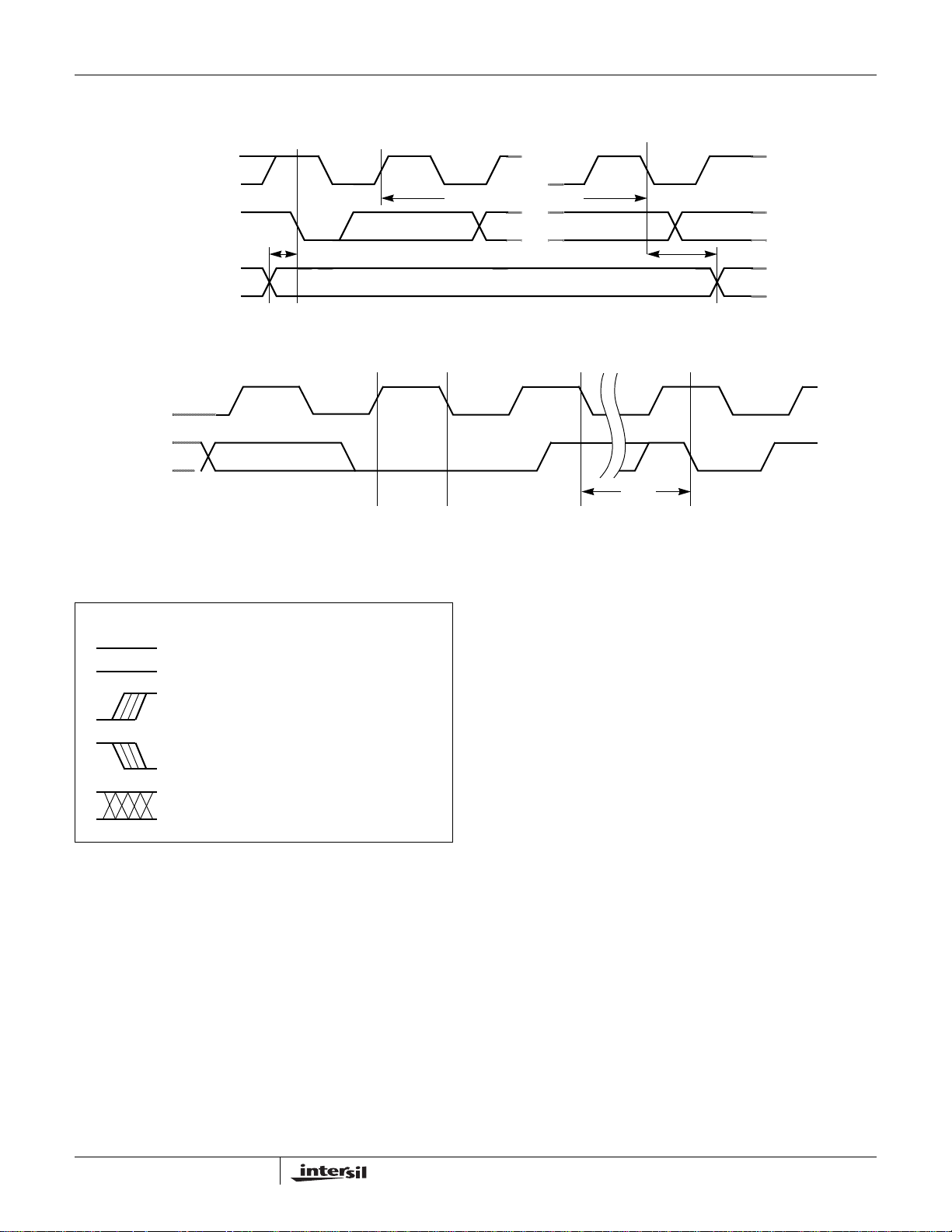
START
X80000, X80001
SCL
SDA
Symbol Table
SCL
SDA IN
WP
t
8th Bit of Last Byte
SU:WP
Clk 1 Clk 9
Slave Address Byte
FIGURE 8. WP PIN TIMING
ACK
Stop
Condition
FIGURE 9. WRITE CYCLE TIMING
t
HD:WP
t
WC
Start
Condition
WAVEFORM INPUTS OUTPUTS
Must be
steady
May change
from LOW
to HIGH
May change
from HIGH
to LOW
Don’t Care:
Changes
Allowed
Will be
steady
Will change
from LOW
to HIGH
Will change
from HIGH
to LOW
Changing:
State Not
Known
11
FN8148.0
March 18, 2005
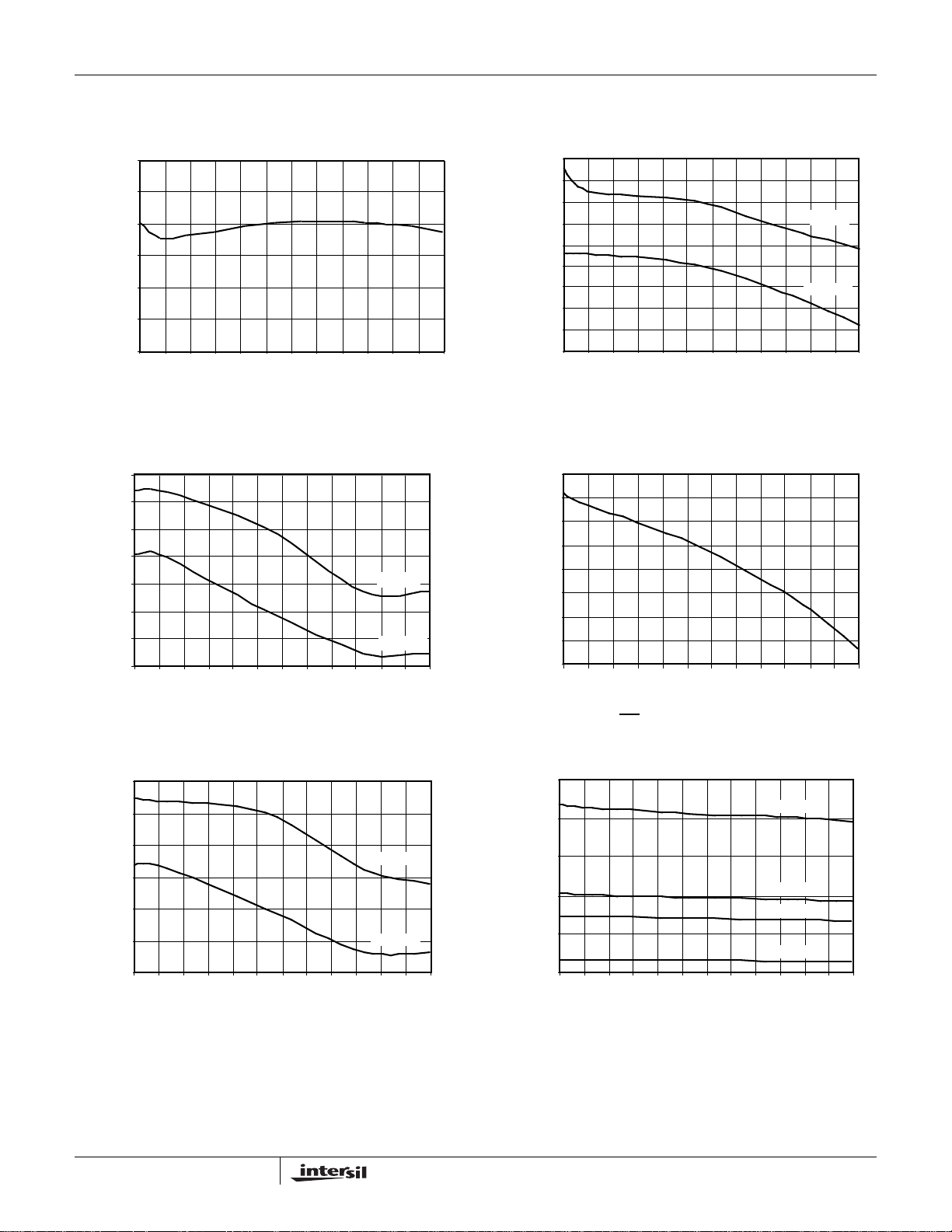
Typical Performance Characteristics
X80000, X80001
52.000
51.000
50.000
49.000
48.000
47.000
INRUSH CURRENT LIMIT (mV)
46.000
-55 -40 -25 -10 5 20 35 50 65 80 95 110 12
TEMPERATURE
1.780
1.770
1.760
1.750
1.740
1.730
1.720
1.710
1.700
UNDERVOLTAGE 2 THRESHOLD (V)
1.690
-55 -40 -25 -10 5 20 35 50 65 80 95 110 125
TEMPERATURE
FIGURE 10. OVERCURRENT THRESHOLD vs TEMPERATURE FIGURE 11. UNDERVOLTAGE 1 THRESHOLD vs
TEMPERATURE
3.92
3.91
3.90
3.89
3.88
3.87
OV THRESHOLD (V)
3.86
3.85
-55 -40 -25 -10 5 20 35 50 65 80 95 110 125
TEMPERATURE
RISING
FALLING
FIGURE 12. OVERVOLTAGE THRESHOLD vs TEMPERATURE FIGURE 13. ENi
2.515
2.510
2.505
2.500
2.495
2.490
2.485
ENi THRESHOLD (V)
2.480
2.475
-55 -40 -25 -10 5 20 35 50 65 80 95 110 125
TEMPERATURE
THRESHOLD vs TEMPERATURE
RISING
FALLING
2.250
2.240
2.230
2.220
2.210
2.200
UNDERVOLTAGE 1 THRESHOLD (V)
2.190
-55 -40 -25 -10 5 20 35 50 65 80 95 110 125
TEMPERATURE
FIGURE 14. UNDERVOLTAGE 1 THRESHOLD vs
TEMPERATURE
12
RISING
FALLING
200
160
120
80
GATE CURRENT (µA)
40
0
-55 -40 -25 -10 5 20 35 50 65 80 95 110 125
TEMPERATURE
FIGURE 15. I
(SOURCE) vs TEMPERATURE
GATE
150µA
70µA
50µA
10µA
FN8148.0
March 18, 2005
