

查询X55060供应商
®
X55060
64K
PRELIMINARY
Data Sheet March 28, 2005
Dual Voltage Monitor with Integrated
System Battery Switch and EEPROM
FEATURES
• Dual voltage monitoring
• Active high and active low reset outputs
• Four standard reset threshold voltages
(4.6/2.9, 4.6/2.6, 2.9/1.6, 2.6/1.6)
—User programmable thresholds
• Lowline Output — Zero delayed POR
• Reset signal valid to V
• System battery switch-over circuitry
• Long battery life with low power consumption
—<50µA max standby current, watchdog on
—<30µA max standby current, watchdog off
• Selectable watchdog timer
—(0.15s, 0.4s, 0.8s, off)
• 64Kbits of EEPROM
• Built-in inadvertent write protection
—Power-up/power-down protection circuitry
—Protect none(0), or all of EEPROM array with
programmable Block Lock
CC
= 1V
™
protection
FN8133.0
—In circuit programmable ROM mode
• Minimize EEPROM programming time
—64 byte page write mode
—Self-timed write cycle
—5ms write cycle time (typical)
• 10MHz SPI interface modes (0,0 & 1,1)
• 2.7V to 5.5V power supply operation
• Available packages — 20-lead TSSOP
DESCRIPTION
This device combines power-on reset control, battery
switch circuit, watchdog timer, supply voltage supervision, secondary voltage supervision, block lock
protect
and serial EEPROM in one package. This combination
lowers system cost, reduces board space requirements, and increases reliability.
Applying power to the device activates the power-on
reset circuit which holds RESET
/RESET active for a
period of time. This allows the power supply and oscillator to stabilize before the processor can execute code.
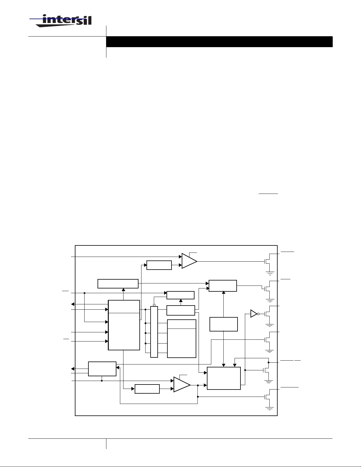
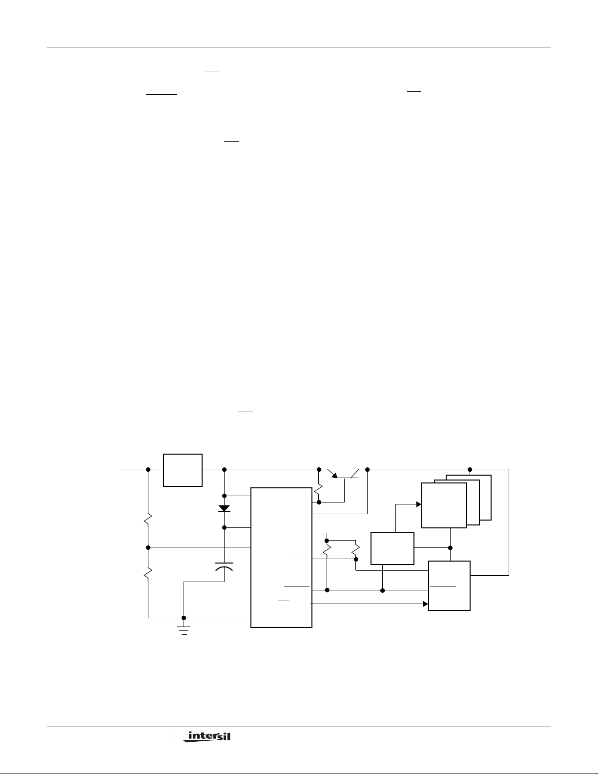
BLOCK DIAGRAM
V2MON
WP
SO
SI
SCK
CS
V
OUT
V
BATT
V
CC
(V1MON)
Watchdog Transition
Detector
Data
Register
Command
Decode, Test
& Control
Logic
System
Battery
Switch
V2 Monitor
X-Decoder
VCC Monitor
Logic
Logic
+
V
TRIP2
-
Protect Logic
Status
Register
EEPROM Array
512 X 128
V
+
V
TRIP1
-
OUT
V
OUT
Watchdog
Timer Reset
Reset &
Watchdog
Timebase
Power-on,
Low Voltage
Reset
Generation
V2FAIL
WDO
RESET
BATT-ON
RESET/MR
LOWLINE
1
CAUTION: These devices are sensitive to electrostatic discharge; follow proper IC Handling Procedures.
1-888-INTERSIL or 1-888-352-6832
| Intersil (and design) is a registered trademark of Intersil Americas Inc.
All other trademarks mentioned are the property of their respective owners.
Copyright Intersil Americas Inc. 2005. All Rights Reserved
X55060
A system battery switch circuit compares VCC (V1MON)
with V
input and connects V
BATT
to whichever is
OUT
higher. This provides voltage to external SRAM or other
circuits in the event of main power failure. The X55060
can drive 50mA from V
device switches to V
low V
voltage threshold and V
CC
and 250µA from V
CC
when VCC drops below the
BATT
BATT
> VCC.
BATT
. The
The Watchdog Timer provides an independent protection mechanism for microcontrollers. When the microcontroller fails to restart a timer within a selectable
time out interval, the device activates the WDO
signal.
The user selects the interval from th ree preset v alues.
Once selected, the interval does not change, even
after cycling the power.
The device’s low V
detection circuitry protects the
CC
user’s system from low voltage conditions, resetting the
system when V
V
trip point (V
CC
V
returns to proper operating level and stabilizes. A
CC
(V1MON) falls below the minimum
CC
). RESET/RESET is asserted until
TRIP1
second voltage monitor circuit tracks the unregulated
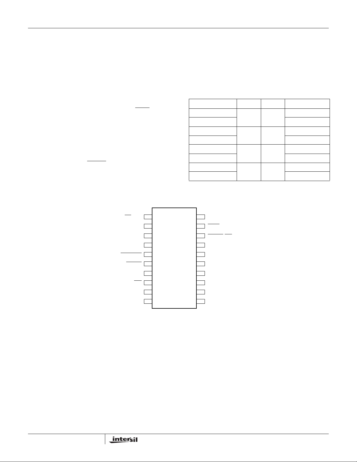
PIN CONFIGURATION
20-Pin TSSOP
supply or monitors a second power supply voltage to
provide a power fail warning. Intersil’s unique circuits
allow the threshold for either voltage monitor to be
reprogrammed to meet special needs or to fine-tune the
threshold for applications requiring higher precision.
ORDERING INFORMATION
X55060
Suffix Vtrip1 Vtrip2 Temp Range
V20-4.5A
V20I-4.5A -40°C to 85°C
V20-4.5
V20I-4.5 -40°C to 85°C
V20-2.7A
V20I-2.7A -40°C to 85°C
V20-2.7
V20I-2.7 -40°C to 85°C
4.6 2.6
4.6 2.9
2.9 1.65
2.6 1.65
0°C to 70°C
0°C to 70°C
0°C to 70°C
0°C to 70°C
CS/WDI
NC
SO
RESET
LOWLINE
V2FAIL
V2MON
WP
NC
VSS
1
2
3
4
5
6
7
8
9
10
20
19
18
17
16
15
14
13
12
11
V
(V1MON)
CC
WDO
/MR
RESET
BATT-ON
V
OUT
V
BATT
SCK
NC
NC
SI
2
FN8133.0
March 28, 2005
X55060
PIN DESCRIPTION
Pin Name Function
1CS
2 NC No internal connections
3SOSerial Output. SO is a push/pull serial data output pin. A read cycle shifts data out on this pin. The
4 RESET Reset Output.
5LOWLINE
6V2FAIL
7V2MONV2 Voltage Monitor Input. When the V2MON input is less than the V
8WP
9 NC No internal connections
10 V
11 SI Serial Input. SI is a serial data input pin. Input all opcodes, byte addresses, and memory data on
12 NC No internal connections
13 NC No internal connections
14 SCK Serial Clock. The Serial Clock controls the serial bus timing for data input and output. The rising
15 V
/WDI
SS
BATT
Chip Select Input. CS HIGH, deselects the device and the SO output pin is at a high impedance
state. Unless a nonvolatile write cycle is underway, the device will be in the standby power mode.
LOW enables the device, placing it in the active power mode. Prior to the start of any opera-
CS
tion after power-up, a HIGH to LOW transition on CS
is required.
Watchdog Input. A HIGH to LOW transition on the WDI pin restarts the Watchdog timer. The
absence of a HIGH to LOW transition within the watchdog time out period results in RESET
going active.
falling edge of the serial clock (SCK) clocks the data out.
RESET is an active HIGH, open drain output which is the inverse of the RESET
output.
Low V
immediately goes HIGH when V
Detect. This open drain output signal goes LOW when VCC < V
CC
CC
> V
. This pin goes LOW 250ns before RESET pin.
TRIP1
TRIP1
and
V2 Voltage Fail Output. This open drain output goes LOW when V2MON is less than V
and goes HIGH when V2MON exceeds V
. There is no power-up reset delay circuitry on this
TRIP2
pin.
voltage, V2FAIL goes
TRIP2
LOW. This input can monitor an unregulated power supply with an external resistor divider or can
monitor a second power supply with no external components. Connect V2MON to V
SS
when not used.
Write Protect. The WP pin works in conjunction with a nonvolatile WPEN bit to “lock” the setting
of the Watchdog Timer control and the memory write protect bits.
Ground
this pin. The rising edge of the serial clock (SCK) latches the input data. Send all opcodes (Table 1),
addresses and data MSB first.
edge of SCK latches in the opcode, address, or data bits present on t he SI pin. The falling e dge of
SCK changes the data output on the SO pin.
Battery Supply Voltage. This input provides a backup supply in the event of a failure of the primary V
voltage. The V
CC
voltage typically provides the supply voltage necessary to maintain
BATT
the contents of SRAM and also powers the internal logic to “stay awake.” If unused connect
V
to ground.
BATT
/RESET
TRIP2
or VCC
3
FN8133.0
March 28, 2005

X55060
PIN DESCRIPTION (CONTINUED)
Pin Name Function
16 V
OUT
17 BATT-ON Battery On. This open drain output goes HIGH when the V
18 RESET
/MR
19 WDO
20 V
CC
(V1MON)
Output Voltage. V
< V
IF V
CC
TRIP1
= VCC if VCC > V
V
OUT
V
OUT
= V
BATT
if VCC < V
Note: There is hysteresis around V
= VCC if VCC > V
OUT
, then,
BATT
BATT
+0.03
-0.03
.
TRIP1
± 0.03V point to avoid oscillation at or near the
BATT
switchover voltage. A capacitance of 0.1µF must be connected to Vout to ensure stability.
when V
switches to VCC. It is used to drive an external PNP pass transistor when VCC = V
OUT
and current requirements are greater than 50mA.
The purpose of this output is to drive an external transistor to get higher operating currents when
the V
the V
supply is fully functional. In the event of a VCC failure, the battery voltage is applied to
CC
pin and the external transistor is turned off. In this “backup condition,” the battery only
OUT
needs to supply enough voltage and current to keep SRAM devices from losing their data-there
is no communication at this time.
Output/Manual Reset Input. This is an Input/Output pin.
RESET
below the minimum V
rupted. RESET
RESET
Output. This is an active LOW, open drain output which goes active whenever VCC falls
sense level. When RESET is active communication to the device is inter-
CC
remains active until VCC rises above the minimum VCC sense level for 150ms.
also goes active on power-up and remains active for 150ms after the power supply
stabilizes.
Input. This is an active LOW debounced input. When MR is active, the RESET/RESET pins
MR
are asserted. When MR
is released, the RESET/RESET remains asserted for t
leased.
Watchdog Output. WDO is an active low, open drain output which goes active whenever the
watchdog timer goes active. WDO
remains active for 150ms, then returns to the inactive state.
Supply Voltage/V1 Voltage Monitor Input. When the V1MON input is less than the VTRIP1
voltage, RESET and RESET go ACTIVE.
switches to V
OUT
and goes LOW
BATT
, and then re-
PURST
OUT
PRINCIPLES OF OPERATION
Power-On Reset
Application of power to the X55060 activates a Poweron Reset Circuit. This circuit goes active at about 1V
and pulls the RESET
/RESET pin active. This signal
prevents the system microprocessor from starting to
operate with insufficient voltage or prior to stabilization
of the oscillator. When V
exceeds the device V
CC
TRIP1
value for 150ms (nominal) the circuit releases
RESET
/RESET, allowing the processor to begin exe-
cuting code.
Low V
During operation, the X55060 monitors the V
and asserts RESET
below a preset minimum V
(V1MON) Voltage Monitoring
CC
/RESET if supply voltage falls
. During this time the
TRIP1
CC
level
communication to the device is interrupted. The
RESET
/RESET signal also prevents the microprocessor from operating in a power fail or brownout condition. The RESET
signal remains active until the
voltage drops below 1V. These also remain active until
V
returns and exceeds V
CC
TRIP1
for t
PURST
.
Low V2MON Voltage Monitoring
The X55060 also monitors a second voltage level and
asserts V2FAIL
mum V
RESET
TRIP2
to prevent the microprocessor from operating
if the voltage falls below a preset mini-
. The V2FAIL signal is either ORed with
in a power fail or brownout condition or used to interrupt the microprocessor with notification of an impending power failure. V2FAIL
returns and exceeds V
The V2MON voltage sensor is powered by V
V
CC
and V
go away (i.e. V
BATT
remains active until V2MON
.
TRIP2
goes away), then
OUT
OUT
. If
V2MON cannot be monitored.
4
FN8133.0
March 28, 2005
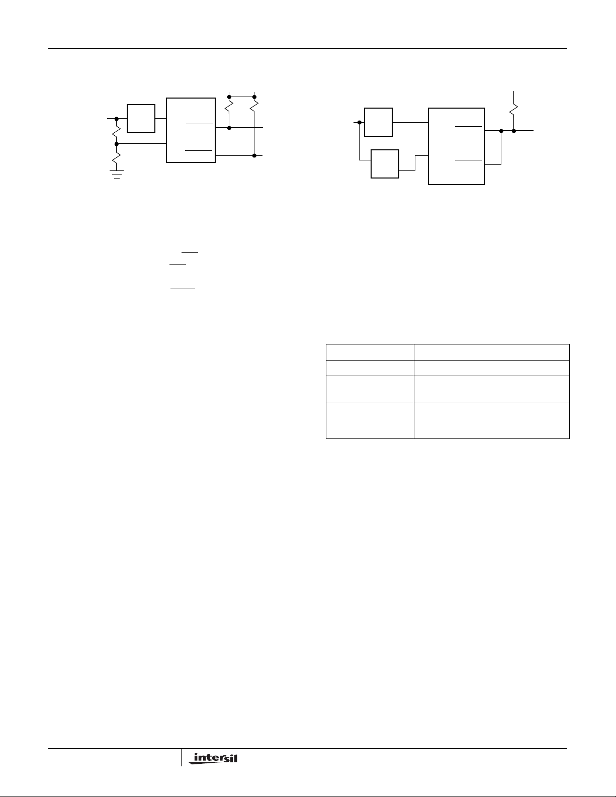
Figure 1. Two Uses of Dual Voltage Monitoring
V
OUT
Unregulated
Supply
R1
R2
V2
5V
Reg
X55060
V
CC
RESET
V2MON
V2FAIL
X55060
System
Reset
System
Interrupt
Unregulated
Supply
5V
Reg
3.3V
Reg
X55060
V
CC
V2MON
RESET
V2FAIL
V
OUT
System
Reset
R1 and R2 selected so V2 = V2MON threshold when
Unregulated supply reaches 6V.
Watchdog Timer
The Watchdog Timer circuit monitors the microprocessor activity by monitoring the CS/
processor must toggle the CS /
WDI pin. The micro-
WDI pin HIGH to LOW
periodically prior to the expiration of the watchdog time
out period to prevent the WDO
signal going active.
The state of two nonvolatile control bits in the Status
Register determines the watchdog timer period. The
microprocessor can change these watchdog bits by
writing to the status register. The factory default setting disables the watchdog timer.
The Watchdog Timer oscillator stops when in battery
backup mode. It re-starts when V
returns.
CC
System Battery Switch
As long as V
old V
TRIP1
(typical) switch. When the V
then V
CC
greater than V
than V
BATT
through an 80Ω (typical) switch. V
exceeds the low voltage detect thresh-
CC
, V
is applied to V
is connected to VCC through a 5Ω
OUT
+ 0.03V. When VCC drops to less
BATT
- 0.03V, then V
has fallen below V
CC
if VCC is equal to or
OUT
is connected to V
OUT
typically sup-
OUT
TRIP
BATT
plies the system static RAM voltage, so the switchover
circuit operates to protect the contents of the static
RAM during a power failure. Typically, when V
CC
has
failed, the SRAMs go into a lower power state and
draw much less current than in their active mode.
When V
V
CC
returns, V
CC
exceeds V
switches back to VCC when
OUT
+ 0.03V. There is a 60mV hyster-
BATT
esis around this battery switch threshold to prevent
oscillations between supplies.
Notice: No external components required to monitor
two voltages.
While V
is connected to V
CC
the BATT-ON pin is
OUT
pulled LOW. The signal can drive an external PNP
transistor to provide additional current to the external
circuits during normal operation.
Operation
The device is in normal operation with V
V
> V
CC
when V
. It switches to the battery backup mode
TRIP1
goes away.
CC
as long as
CC
Condition Mode of Operation
VCC > V
V
> V
CC
= 0
V
BATT
0 ≤ V
CC VTRIP1
and V
CC
TRIP1
TRIP1
< V
&
BATT
Normal Operation.
Normal Operation without battery
back up capability.
Battery Backup Mode; RESET
signal is asserted. No communication to the device is allowed.
,
5
FN8133.0
March 28, 2005
X55060
Manual Reset
By connecting a push-button from MR
to ground or
driven by logic, the designer adds manual system reset
capability. The RESET/RESET
the push-button is closed and remain asserted for t
pins are asserted when
PURST
after the push-button is released. This pin is debounced
so a push-button connected directly to the device will
have both clean falling and rising edges on MR
V
(V1MON), V2MON Threshold Programming
CC
.
Procedure
The X55060 is shipped with standard V
and V2MON threshold (V
TRIP1
, V
CC
TRIP2
(V1MON)
) voltages.
These values will not change over normal operating
and storage conditions. However, in applications where
the standard thresholds are not exactly right, or if higher
precision is needed in the threshold value, the X55060
trip points may be adjusted. The procedure is described
below, and uses the application of a high voltage control signal.
Setting the V
This procedure is used to set the V
TRIP
Voltage
TRIP1
or V
TRIP2
to a
lower or higher voltage value. It is necessary to reset
the trip point before setting the new value to a lower
level.
To set the new voltage, apply the desired V
threshold voltage to the VCC pin or the V
to the V2MON pin (when setting V
TRIP2
, VCC should
TRIP2
be same voltage as V2MON). Next, tie the WP
TRIP1
voltage
pin to
the programming voltage V
. Then, send the WREN
P
command and write to address 01h or to add ress 0Bh
to program V
data byte 00h). The CS
TRIP1
or V
, respectively (followed by
TRIP2
going high after a valid write
operation initiates the programming sequence. Bring
WP
LOW to complete the operation.
To check if the V
higher than V
TRIPX
has been set, apply a voltage
TRIPX
to the VXMON (x = 1, 2) pin. Decrement VXMON in small steps and observe where the
output switches. The voltage at which this occurs is
the V
C
ASE A
If the V
(desired), then add the difference between V
(desired) and V
(desired). This is your new V
TRIPX
(actual).
(actual) is lower than the V
TRIPX
(actual) to the original V
TRIPX
voltage that should
TRIPX
TRIPX
TRIPX
TRIPX
be applied to VXMON and the whole sequence
repeated again (see Fig 6).
C
ASE B
If the V
(actual) is higher than the V
TRIPX
TRIPX
(desired), perform the reset sequence as described in
the next section. The new V
to VXMON will now be: V
(desired) - V
TRIPX
(actual)).
voltage to be applied
TRIPX
(desired) - (V
TRIPX
TRIPX
Note: This operation will not alter the contents of the
EEPROM.
Figure 2. Example System Connection
Unregulated
Supply
5V
Reg
+
V
CC
V
BATT
V2MON
V
SS
BATT-ON
V
OUT
V2FAIL
RESET
CS, SCK
SI, SO
PNP transistor
or P-channel FET
V
OUT
Address
Decode
Enable
SRAM
Addr
NMI
RESET
SPI
µC
V
CC
6
FN8133.0
March 28, 2005
X55060
Resetting the V
To reset V
TRIP1
(V1MON). To reset V
both V
and V2MON. Next, tie the WP pin to the
CC
programming voltage V
Voltage
TRIP
, apply greater than 3V to V
, apply greater than 3V to
TRIP2
. Then send the WREN
P
CC
command and write to address 03h or 0Dh to reset th e
V
or V
TRIP1
Figure 3. Set V
WP
CS
SCK
SI
respectively (followed by data byte
TRIP2
Level Sequence
TRIPX
01234567 0123456
06h
WREN
WRITE
VP = 10-15V
02h
00h). The CS
going LOW to HIGH after a valid write
operation initiates the programming sequence. Bring
WP
LOW to complete the operation.
Note: This operation does not change the contents of
the EEPROM array.
78910 202122 23
16 Bits
0001h/000Bh
ADDRESS
Addr 01h: Set V
Addr 0Bh: Set V
TRIP1
TRIP2
00h
DATA
Figure 4. Reset V
WP
CS
01234567 0123456
SCK
SI
Level Sequence
TRIPX
06h
WREN
VP = 10-15V
02h
WRITE
78910 202122 23
16 Bits
0003h/000Dh
ADDRESS
Addr 03h: Reset V
Addr 0Dh: Reset V
00h
DATA
TRIP1
TRIP2
7
FN8133.0
March 28, 2005

X55060
Figure 5. Sample V
V
TRIP
Adj.
Figure 6. V
Programming Sequence Flow Chart
TRIP
TRIP
Circuit
4.7K
V
P
Adjust
Run
CS
SO
WP
V
SS
X55060
RESET
V
CC
SCK
SI
RESET
µC
SCK
SI
SO
CS
V
TRIPX
Programming
Vx = VxMON
Note: X = 1, 2
Let: MDE = Maximum Desired Error
No
Desired
V
TRIPX
Present Value?
Execute
V
Reset Sequence
TRIPX
<
YES
MDE
Desired Value
MDE
+
Acceptable
Error Range
–
Error = Actual - Desired
New VX applied =
applied + | Error |
Old V
X
Error < MDE
NO
VX = desired V
Execute
Set Higher
Apply V
> Desired V
Decrease
V
TRIPX
and Voltage
CC
TRIPX
TRIPX
Sequence
to
V
X
V
X
New VX applied =
Old V
applied - | Error |
X
Execute Reset V
Sequence
TRIPX
Output Switches?
YES
Set
–
Actual
Desired
V
TRIPX -
V
TRIPX
Error > MDE
+
| Error | < | MDE |
DONE
8
FN8133.0
March 28, 2005

X55060
SPI SERIAL MEMORY
The memory portion of the device is a CMOS Serial
EEPROM array with Intersil’s block lock protection. The
array is internally organized as x 8. The device features
a Serial Peripheral Interface (SPI) and software protocol allowing operation on a simple four-wire bus.
The device utilizes Intersil’s proprietary Direct Write
™
cell, providing a minimum endurance of 100,000
cycles and a minimum data retention of 100 years.
The device is designed to interface directly with the
synchronous Serial Peripheral Interface (SPI) of many
popular microcontroller families. It contains an 8-bit
instruction register that is accessed via the SI input,
with data being clocked in on the rising edge of SCK.
CS
must be LOW during the entire operation.
All instructions (Table 1), addresses and data are
transferred MSB first. Data input on the SI line is
latched on the first rising edge of SCK after CS
goes
LOW. Data is output on the SO line by the falling edge
of SCK. SCK is static, allowing the user to stop the
clock and then start it again to resume operations
where left off.
Write Enable Latch
The device contains a Write Enable Latch. This latch
must be SET before a Write Operation is initiated. The
WREN instruction sets the latch and the WRDI instruction resets the latch (Figure 9). This latch is automatically reset upon a power-up condition and after the
completion of a valid Write Cycle.
Status Register
The RDSR instruction provides access to the Status
Register. The Status Register may be read at any
time, even during a Write Cycle. The Status Register
is formatted as follows:
76543210
WPEN WD1 WD0 PUP BL1 BL0 WEL WIP
The Write-In-Progress (WIP) bit is a volatile, read only
bit and indicates whether the device is busy with an
internal nonvolatile write operation. The WIP bit is read
using the RDSR instruction. When set to a “1”, a nonvolatile write operation is in progress. When set to a
“0”, no write is in progress.
Table 1. Instruction Set
Instruction Name Instruction Format* Operation
WREN 0000 0110 Set the Write Enable Latch (Enable Write Operations)
WRDI 0000 0100 Reset the Write Enable Latch
RSDR 0000 0101 Read Status Register
WRSR 0000 0001 Write Status Register (Watchdog, block lock, WPEN)
READ 0000 0011 Read Data from Memory Array Beginning at Selected Address
WRITE 0000 0010 Write Data to Memory Array Beginning at Selected Address
Note: *Instructions are shown MSB in leftmost position. Instructions are transferred MSB first.
Table 2. Block Protect Matrix
WREN CMD Status Register Device Pin Block Block Status Register
WPEN, BL0, BL1,
WEL WPEN WP
0 X X Protected Protected Protected
1 1 0 Protected Writable Protected
1 0 X Protected Writable Writable
1 X 1 Protected Writable Writable
Protected Block Unprotected Block
PUP, WD0, WD1
9
FN8133.0
March 28, 2005
X55060
The Write Enable Latch (WEL) bit indicates the Status
of the Write Enable Latch. When WEL = 1, the latch is
set HIGH and when WEL = 0 the latch is reset LOW.
The WEL bit is a volatile, read only bit. It can be set by
the WREN instruction and can be reset by the WRDS
instruction.
The block lock bits, BL0 and BL1, set the level of block
lock protection. These nonvolatile bits are programmed using the WRSR instruction and allow the
user to protect one quarter, one half, all or none of the
EEPROM array. Any portion of the array that is block
lock protected can be read but not written. It will
remain protected until the BL bits are altered to disable
block lock protection of that portion of memory.
Status Register Bits Array Addresses Protected
BL1 BL0 X55060
0 0 None (factory setting)
0 1 None
1 0 None
1 1 0000h–1FFFh (All)
The power-on reset time (t
) bit, PUP sets the
PURST
initial power or reset time. There are two standard
settings.
PUP Time
0 150 milliseconds (factory settings)
1 800 milliseconds
The Watchdog Timer bits, WD0 and WD1, select the
Watchdog Time-out Period. These nonvolatile bits are
programmed with the WRSR instruction.
Status Register Bits
Watchdog Time Out
(Typical)WD1 WD0
0 0 800 milliseconds
0 1 400 milliseconds
1 0 150 milliseconds
1 1 disabled (factory setting)
The nonvolatile WPEN bit is programmed using the
WRSR instruction. This bit works in conjunction with
the WP
ROM function (Table 2). WP
pin to provide an In-Circuit Programmable
tied to VSS and WPEN bit
programmed HIGH disables all Status Register Write
Operations.
Note 1. Watchdog timer is shipped disabled.
2. The t
time is set to 150ms at the factory.
PURST
In Circuit Programmable ROM Mode
This mechanism protects the block lock and Watchdog
bits from inadvertent corruption.
In the locked state (Programmable ROM Mode) the
WP
pin is LOW and the nonvolatile bit WPEN is “1”.
This mode disables nonvolatile writes to the device’s
Status Register.
Setting the WP
pin LOW while WPEN is a “1” while an
internal write cycle to the Status Register is in progress
will not stop this write operation, but the operation disables subsequent write attempts to the Status Register.
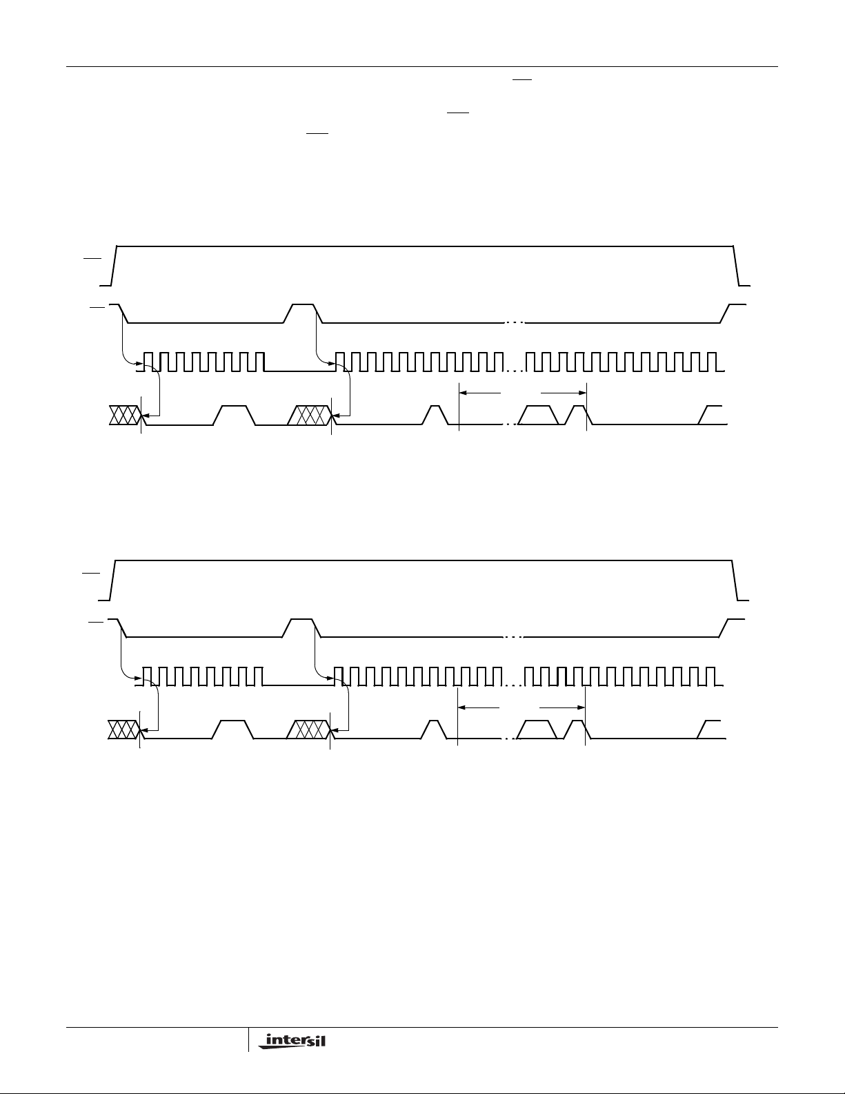
Figure 7. Read EEPROM Array Sequence
CS
0 1 2 3 4 5 6 7 8 9 10 20 21 22 23 24 25 26 27 28 29 30
SCK
Instruction 16 Bit Address
SI
SO
High Impedance
10
15 14 13 3 2 1 0
Data Out
76543210
MSB
FN8133.0
March 28, 2005

X55060
When WP is HIGH, all functions, including nonvolatile
writes to the Status Register opera te norm ally. Setting
the WPEN bit in the Status Register to “0” blocks the
WP
pin function, allowing writes to the Status Register
when WP
“1” while the WP
ble ROM mode, thus requiring a ch an ge in t he WP
is HIGH or LOW. Setting the WPEN bit to
pin is LOW activates the Programma-
pin
prior to subsequent Status Register changes. This
allows manufacturing to install the device in a system
with WP
pin grounded and still be able to program the
Status Register. Manufacturing can then load Configuration data, manufacturing tim e and other parameters
into the EEPROM, then set the portion of memory to
be protected by setting the block lock bits, and finally
set the “OTP mode” by setting the WPEN bit. Data
changes to protected areas of the device now require
a hardware change.
Read Sequence
When reading from the EEPROM memory array, CS
is
first pulled low to select the device. The 8-bit READ
instruction is transmitted to the device, followed by the
16-bit address. After the READ opcode and address
are sent, the data stored in the memory at the selected
address is shifted out on the SO line. The data stored in
memory at the next address can be read sequentially
by continuing to provide clock pulses. The address is
automatically incremented to the next higher address
after each byte of data is shifted out. The read operation
is terminated by taking CS
high. Refer to the Read
EEPROM Array Sequence (Figure 7).
To read the Status Register, the CS
line is first pulled
low to select the device followed by the 8-bit RDSR
instruction. After the RDSR opcode is sent, the contents
of the Status Register are shifted out on the SO line.
Refer to the Read Status Register Sequence (Figure 8).
Refer to the Serial Output Timing on page 18.
Write Sequence
Prior to any attempt to write data into the device, the
“Write Enable” Latch (WEL) must fi rst be set by issuing the WREN instruction (Figure 9). CS
is first taken
LOW, then the WREN instruction is clocked into the
device. After all eight bits of the instruction are transmitted, CS
tinues the Write Operation without taking CS
must then be taken HIGH. If the user con-
HIGH
after issuing the WREN instruction, the Write Operation will be ignored.
To write data to the EEPROM memory array, the user
then issues the WRITE instruction followed by the 16
bit address and then the data to be written. Any
unused address bits are specified to be “0’s”. The
WRITE operation minimally takes 32 clocks. CS
must
go low and remain low for the duration of the operation. If the address counter reaches the end of a page
and the clock continues, the counter will roll back to
the first address of the page and overwrite any data
that may have been previously written.
For the Page Write Operation (byte or page write) to
be completed, CS
can only be brought HIGH after bit 0
of the last data byte to be written is clocked in. If it is
brought HIGH at any other time, the write operation
will not be completed (Figure 10).
To write to the Status Register, the WRSR instruction
is followed by the data to be written (Figure 11) .
While the write is in progress following a Status Register or EEPROM Sequence, the Status Register may
be read to check the WIP bit. During this time the WIP
bit will be high. Refer to Serial Input timing on page 17.
OPERATIONAL NOTES
The device powers-up in the following state:
– The device is in the low power standby state.
– A HIGH to LOW transition on CS
is required to enter
an active state and receive an instruction.
– SO pin is high impedance.
– The Write Enable Latch is reset.
– Reset Signal is active for t
PURST
.
Data Protection
The following circuitry has been included to prevent
inadvertent writes:
– A WREN instruction must be issued to set the Write
Enable Latch.
– A valid write command and address must be sent to
the device.
–CS
must come HIGH after a multiple of 8 data bits in
order to start a nonvolatile write cycle.
11
FN8133.0
March 28, 2005

Figure 8. Read Status Register Sequence
CS
01234567891011121314
SCK
Instruction
SI
X55060
SO
High Impedance
Figure 9. Write Enable Latch Sequence
CS
SCK
SI
SO
High Impedance
Data Out
76543210
MSB
01234567
12
FN8133.0
March 28, 2005

Figure 10. Write Sequence
CS
X55060
012345678910
SCK
Instruction 16 Bit Address
SI
CS
32 33 34 35 36 37 38 39
SCK
Data Byte 2
SI
76543210
Figure 11. Status Register Write Sequence
CS
0123456789
SCK
20 21 22 23 24 25 26 27 28 29 30 31
15 14 13 3 2 1 0
40 41 42 43 44 45 46 47
Data Byte 3
76543210
10 11 12 13 14 15
Data Byte 1
76543210
Data Byte N
654 3210
SI
SO
High Impedance
Symbol Table
WAVEFORM INPUTS OUTPUTS
Must be
steady
May change
from LOW
to HIGH
May change
from HIGH
to LOW
Don’t Care:
Changes
Allowed
N/A Center Line
Will be
steady
Will change
from LOW
to HIGH
Will change
from HIGH
to LOW
Changing:
State Not
Known
is High
Impedance
Instruction
Data Byte
76543210
13
FN8133.0
March 28, 2005

X55060
ABSOLUTE MAXIMUM RATINGS
Temperature under bias ...................-65°C to +135°C
Storage temperature ........................-65°C to +150°C
Voltage on any pin with
respect to V
...................................... -1.0V to +7V
SS
D.C. output current
(all output pins except V
D.C. Output Current V
OUT
).............................5mA
OUT
..................................50mA
COMMENT
Stresses above those listed under “Absolute Maximum
Ratings” may cause permanent damage to the device.
This is a stress rating only; the functional operation of the
device (at these or any other conditions above those
listed in the operational sections of this specification) is
not implied. Exposure to absolute maximum rating conditions for extended periods may affect device reliability.
Lead temperature (soldering, 10 seconds)........ 300°C
RECOMMENDED OPERATING CONDITIONS
Temperature Min. Max.
Commercial 0°C 70°C
Industrial -40°C +85°C
D.C. OPERATING CHARACTERISTICS
(Over recommended operating conditions unless otherwise specified. (V
Limits
Symbol Parameter
(1)
I
CC1
I
CC2
I
CC3
I
BATT1
I
BATT2
)
VCC Supply Current (Active)
(Excludes I
(Excludes I
(2)
VCC Supply Current (Passive)
(Excludes I
(Excludes I
(Excludes I
(1)
VCC Current (Battery Backup Mode)
(Excludes I
(3)(7
V
Current (Excludes I
BATT
(7)
V
Current (Excludes I
BATT
) Read Memory array
OUT
) Write nonvolatile Memory
OUT
) WDT on, 5V
OUT
) WDT on, 2.7V
OUT
) WDT off, 5V
OUT
)
OUT
50.0
40.0
30.0
)1µAV
OUT
) (Battery
OUT
0.4 1.0 µA V
Backup Mode)
(7)
V
V
OUT1
OUT2
V
OLB
V
BSH
Output Voltage (VCC > V
> V
V
CC
TRIP1
(7)
Output Voltage (VCC < V
< V
V
CC
TRIP1
)
) {Battery Backup}
BATT
BATT
+ 0.03V or
-0.03V and
Output (BATT-ON) LOW Voltage 0.4 V IOL = 3.0mA (5V)
Battery Switch Hysteresis
(V
CC
< V
TRIP1
)
V
- 0.05
CC
- 0.5
V
CC
V
- 0.2 VVI
BATT
RESET/RESET/LOWLINE/WDO
(6)
V
TRIP1
VCC Reset Trip Point Voltage 4.5 4.62 4.75 V -4.5A and -4.5 versions
2.85 3.0 V -2.7A version
2.55 2.75 V -2.7 version
V
OLR
Output (RESET, RESET, LOWLINE,
) LOW Voltage
WDO
= 2.7V to 5.5V))
CC
(5)
Max.
1.5
3.0
90.0
60.0
50.0
1µAV
V
-0.02
CC
-0.2VV
V
CC
30
-30
0.4 V I
Unit Test ConditionsMin. Typ.
mA SCK = V
0.9 @ 10MHz
µA CS
= VCC, Any Input =
or VCC, V
V
SS
RESET, RESET
LOWLINE
= 2V, V
CC
2.8V, V
Open
= V
OUT
= V
OUT
V
BATT
, RESET = Open
V
OUT
I
= -5mA
OUT
= -50mA
I
OUT
= -250µA
OUT
= 1.0mA (3V)
I
OL
mVmVPower-up
Power-down
= 3.0mA (5V)
OL
= 1.0mA (3V)
I
OL
x 0.1/V
CC
= Open
BATT
, RESET =
OUT
Bt
BATT
=2.8V
OUT
,
x
CC
,
,
=
14
FN8133.0
March 28, 2005

X55060
D.C. OPERATING CHARACTERISTICS (CONTINUED)
(Over recommended operating conditions unless otherwise specified. (V
Limits
Symbol Parameter
Second Supply Monitor
(6)
V
TRIP2
V
OLx
SPI Interface
V
ILx
V
IHx
I
LIx
V
OLS
V
OHS
V2MON Reset Trip Point Voltage 2.85 3.0 V -4.5 version
2.55 2.7 V -4.5A version
1.6 1.7 V -2.7A and -2.7 version
Output (V2FAIL) LOW Voltage 0.4 V IOL = 3.0mA (5V)
(4)
Input (CS, SI, SCK, WP) LOW Voltage -0.5 VCC x 0.3 V
(4)
Input (CS, SI, SCK, WP) HIGH Voltage VCC x 0.7 VCC + 0.5 V
Input Leakage Current (CS, SI, SCK,WP) ±10 µA
Output (SO) LOW Voltage 0.4 V IOL = 3.0mA (5V)
Output (SO) HIGH Voltage V
- 0.8 V IOH = -1.0mA (5V)
OUT
= 2.7V to 5.5V))
CC
(5)
Max.
Unit Test ConditionsMin. Typ.
= 1.0mA (3V)
I
OL
= 1.0mA (3V)
I
OL
Notes: (1) The device enters the Active state after any start, and remains active until 9 clock cycles late r if the Device Select Bits in the Slave
Address Byte are incorrect; 200ns after a stop ending a read operation; or t
(2) The device goes into Standby: 200ns after any Stop, except those that initiate a high voltage write cycle; t
high voltage cycle; or 9 clock cycles after any start that is not followed by the correct Device Select Bits in the Slave Address Byte.
(3) Negative number indicate charging current, Positive numbers indicate discharge current.
(4) V
min. and VIH max. are for reference only and are not tested.
IL
(5) V
= 5V at 25°C.
CC
(6) V
(7) Based on characterization data.
and V
TRIP1
cedure. For custom programmed levels, contact factory.
are programmable. See page 22 and 23 for programming specifications and pages 6, 7 and 8 for programming pro-
TRIP2
after a stop ending a write operation.
WC
WC
after a stop that initiates a
CAPACITANCE TA = +25°C, f = 1MHz, VCC = 5V
Symbol Test Max. Unit Conditions
(1)
C
OUT
C
IN
Note: (1) This parameter is periodically sampled and not 100% tested.
Output Capacitance (SO, RESET, V2FAIL, RESET, LOWLINE, BATT-ON,WDO)8 pFV
(1)
Input Capacitance (SCK, SI, CS, WP)6pFV
OUT
IN
= 0V
= 0V
15
FN8133.0
March 28, 2005

X55060
EQUIVALENT A.C. LOAD CIRCUIT AT 5V V
SO
3.03kΩ
V
OUT
2.06kΩ
RESET/RESET
BATT-ON/LOWLINE/
V2FAIL
30pF
, WDO
V
OUT
CC
1.53kΩ
30pF
A.C. TEST CONDITIONS
Input pulse levels VCC x 0.1 to VCC x 0.9
Input rise and fall times 10ns
Input and output timing level V
CC
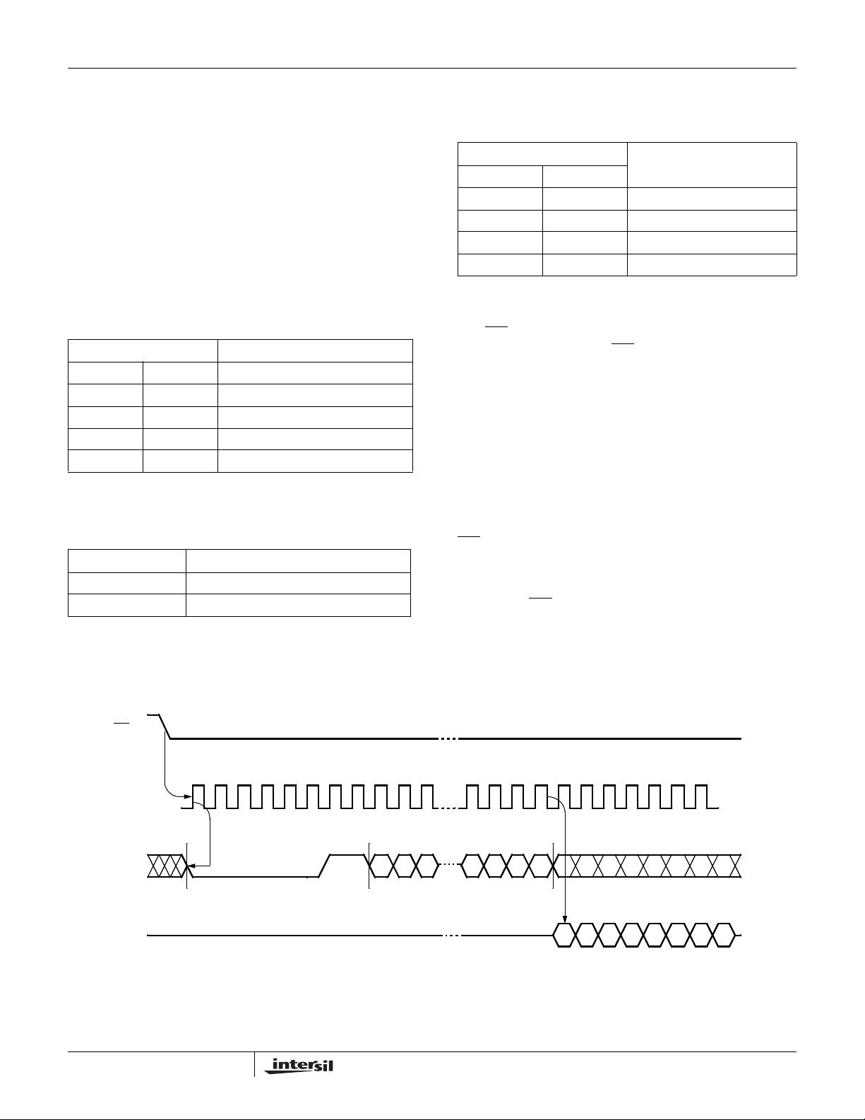
A.C. CHARACTERISTICS (Over recommended operating conditions, unless otherwise specified)
Serial Input Timing
= 2.7-5.5V
V
CC
Symbol Parameter
f
SCK
t
CYC
t
LEAD
t
LAG
t
WH
t
WL
t
SU
t
t
RI
t
FI
t
CS
t
WC
H
(3)
(3)
(4)
Clock Frequency 10 MHz
Cycle Time 100 ns
CS Lead Time 50 ns
CS Lag Time 200 ns
Clock HIGH Time 40 ns
Clock LOW Time 40 ns
Data Setup Time 10 ns
Data Hold Time 10 ns
Input Rise Time 20 ns
Input Fall Time 20 ns
CS Deselect Time 50 ns
Write Cycle Time 10 ms
x0.5
UnitMin. Max.
16
FN8133.0
March 28, 2005

Serial Input Timing
CS
X55060
t
CS
t
LEAD
SCK
SO
t
SU
SI
MSB IN
High Impedance
t
H
Serial Output Timing
Symbol Parameter
t
t
f
SCK
t
DIS
t
t
HO
RO
FO
V
(3)
(3)
Clock Frequency 10 MHz
Output Disable Time 50 ns
Output Valid from Clock Low 40 ns
Output Hold Time 0 ns
Output Rise Time 25 ns
Output Fall Time 25 ns
t
LAG
t
RI
t
FI
LSB IN
2.7-5.5V
UnitMin. Max.
Notes: (3) This parameter is periodically sampled and not 100% tested.
(4) t
is the time from the rising edge of CS after a valid write sequence has been sent to the end of the self-timed internal nonvolatile
WC
write cycle.
17
FN8133.0
March 28, 2005

Serial Output Timing
CS
X55060
SCK
t
V
SO
SI
ADDR
LSB IN
MSB Out MSB–1 Out LSB Out
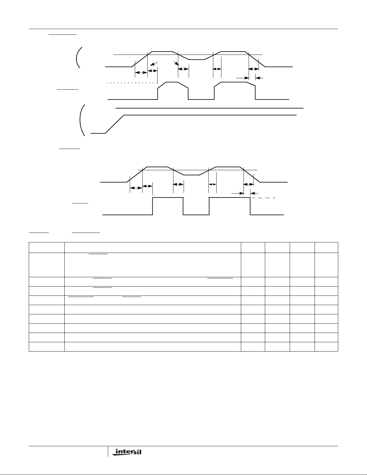
Power-Up and Power-Down Timing
V
V
CC
RESET
V
OUT
TRIP1
0V
t
t
CYC
PURST
t
WH
t
HO
t
PURST
t
WL
t
RPD
t
V
V
V
LAG
t
DIS
BATT
CC
BAT
0V
RESET
BATT-ON
18
t
VB1
t
VB2
V
OUT
V
OUT
FN8133.0
March 28, 2005
VCC to LOWLINE Timings
X55060
V
CC
LOWLINE
V
BATT
V2MON to V2FAIL
V2MON
V2FAIL
V
TRIP1
0V
V
OH
V
OL
V
TRIP1
0V
Timings
0V
V
t
RPD
t
R
t
RPD2
t
R
t
RPD2
t
RPD
t
F
TRIP
V
TRIP2
t
F
V
OUT
RESET
/RESET/LOWLINE Output Timing
Symbol Parameter Min. Typ.
t
PURST
(1)
t
RPD
t
RPD2
t
LR
(2)
t
F
(2)
t
R
V
RVALID
t
VB1
t
VB2
Notes: (1) This parameter is not 100% tested.
(2) This measurement is from 10% to 90% of the supply voltage.
(3) V
(4) Based on characterization data only.
RESET/RESET Time-out Period
(1)
PUP = 0
PUP = 1
V
to RESET/RESET (Power-down only) V
TRIP1
V
to V2FAIL 10 20 µs
TRIP2
to LOWLINE 10 20 µs
TRIP1
75
500
LOWLINE to RESET/RESET delay (Power-down only) 100 250
VCC/V2MON Fall Time 1000 µs
VCC/V2MON Rise Time 1000 µs
Reset Valid V
V
BATT
V
BATT
= 5V at 25°C.
CC
CC
+ 0.03 v to BATT-ON (logical 0) 20
- 0.03 v to BATT-ON (logical 1) 20
1V
150
800
(3)
(4)
Max. Unit
250
ms
1200
800 ns
(4)
(4)
µs
µs
19
FN8133.0
March 28, 2005
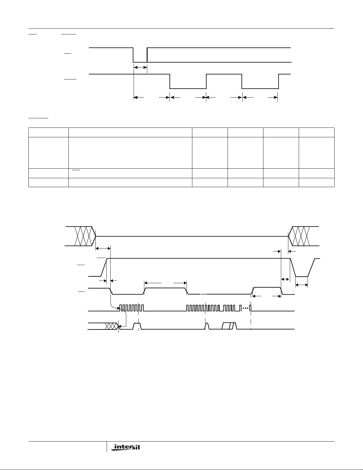
CS/WDI vs. WDO Timing
CS/WDI
WDO
t
X55060
CST
t
WDO
RESET
/RESET Output Timing
t
WDO
t
RST
Symbol Parameter Min. Typ.
t
WDO
t
CST
t
RST
Notes: (1) VCC = 5V at 25°C.
(2) Based on characterization data only.
V
Set/Reset Conditions
TRIP
VCC/V2MON
Watchdog Time Out Period,
WD1 = 1, WD0 = 0
WD1 = 0, WD0 = 1
WD1 = 0, WD0 = 0
75
200
500
CS Pulse Width to Reset the Watchdog 400 ns
Reset Time Out 75 150 250 ms
V
TRIPX
t
TSU
V
P
WP
150
400
800
(2)
(2)
(1)
t
RST
Max. Unit
250
600
1200
t
THD
ms
ms
ms
CS
SCK
SI
X = 1, 2
20
t
VPS
06h
t
PCS
02h
* 0001h Set V
* 0003h Set V
* 000Bh Reset V
* 000Dh Reset V
TRIP1
TRIP2
8
clocks
0n
TRIP1
TRIP2
t
VPH
t
WC
* all others reserved
t
VPO
FN8133.0
March 28, 2005

X55060
V
, V
TRIP1
Parameter Description Min. Max. Unit
t
VPS
t
VPH
t
TSU
t
THD
t
WC
t
VPO
V
P
V
TRAN
V
tv
V
TRIPX
Programming Specifications V
TRIP2
WP V
WP V
V
TRIPX
V
TRIPX
V
TRIPX
WP V
Program Voltage Setup time 10 µs
TRIPX
Program Voltage Hold time 10 µs
TRIPX
Level Setup time 10 µs
Level Hold (stable) time 10 ms
Write Cycle Time 10 ms
Program Voltage Off time before next cycle 1 ms
TRIPX
= 2.7-5.5V; Temperature = 25°C
CC
Programming Voltage 10 15 V
V
Programed Voltage Range 2.5 5.0 V
TRIPX
V
Program variation after programming (0–75°C). (Programmed at 25°C ac-
TRIPX
-25 +25 mV
cording to the procedure defined on pages 6, 7 and 8.)
programming parameters are periodically sampled and are not 100% tested.
21
FN8133.0
March 28, 2005

PACKAGING INFORMATION
X55060
20-Lead Plastic, TSSOP, Package Type V
.025 (.65) BSC
.0075 (.19)
.0118 (.30)
0° - 8°
.193 (4.9)
.200 (5.1)
.019 (.50)
.029 (.75)
Detail A (20X)
.169 (4.3)
.177 (4.5)
.047 (1.20)
.002 (.05)
.006 (.15)
.010 (.25)
Gage Plane
Seating Plane
.252 (6.4) BSC
.031 (.80)
.041 (1.05)
See Detail “A”
NOTE: ALL DIMENSIONS IN INCHES (IN PARENTHESES IN MILLIMETERS)
22
FN8133.0
March 28, 2005

Part Mark Information
X55060
X55060
YYww
Date
Code
W
V20 = 20-Lead TSSOP
X
Part
Mark
V
TRIP1
Range
V
TRIP2
Range
Operating
Temperature Range Part Number
Blank 4.5-4.75V 2.55-2.7V 0°C-70°C X55060V20-4.5A
I -40°C-85°C X55060V20I-4.5A
AL 4.5-4.75V 2.85-3.0V 0°C-70°C X55060V20-4.5
AM -40
°
C-85°C X55060V20I-4.5
F 2.85-3.0V 1.6-1.7V 0°C-70°C X55060V20-2.7A
G-40
°
C-85°C X55060V20I-2.7A
AN 2.55-2.75V 1.6-1.7V 0°C-70°C X55060V20-2.7
AP -40
°
C-85°C X55060V20I-2.7
All Intersil U.S. products are manufactured, assembled and tested utilizing ISO9000 quality systems.
Intersil Corporation’s quality certifications can be viewed at www.intersil.com/design/quality
Intersil products are sold by description only. Intersil Corporation reserves the right to make changes in circuit design, software and/or specifications at any time without
notice. Accordingly, the reader is cautioned to verify that data sheets are current before placing orders. Information furnished by Intersil is believed to be accurate and
reliable. However, no responsibility is assumed by Intersil or its subsidiaries for its use; nor for any infringements of patents or other rights of third parties which may result
from its use. No license is granted by implication or otherwise under any patent or patent rights of Intersil or its subsidiaries.
For information regarding Intersil Corporation and its products, see www.intersil.com
23
FN8133.0
March 28, 2005
 Loading...