

®
www.BDTIC.com/Intersil
X28C010, X28HT010
Data Sheet February 12, 2007
5V, Byte Alterable EEPROM
The Intersil X28C010/X28HT010 is a 128K x 8 EEPROM,
fabricated with Intersil's proprietary, high performance,
floating gate CMOS technology. Like all Intersil
programmable non-volatile memories, the
X28C010/X28HT010 is a 5V only device. The
X28C010/X28HT010 features the JEDEC approved pin out
for byte-wide memories, compatible with industry standard
EEPROMs.
The X28C010/X28HT010 supports a 256-byte page write
operation, effectively providing a 19µs/byte write cycle and
enabling the entire memory to be typically written in less
than 2.5 seconds. The X28C010/X28HT010 also features
DATA Polling and Toggle Bit Polling, system software
support schemes used to indicate the early completion of a
write cycle. In addition, the X28C010/X28HT010 supports
Software Data Protection option.
Intersil EEPROMs are designed and tested for applications
requiring extended endurance. Data retention is specified to
be greater than 100 years.
FN8105.1
Features
• Access time: 120ns
• Simple byte and page write
- Single 5V supply
cell
control
PP
- No external high voltages or V
circuits
- Self-timed
• No erase before write
• No complex programming algorithms
• No overerase problem
• Low power CMOS
- Active: 50mA
- Standby: 500µA
• Software data protection
- Protects data against system level inadvertent writes
• High speed page write capability
• Highly reliable Direct Write
™
- Endurance: 100,000 write cycles
- Data retention: 100 years
• Early end of write detection
-DATA
polling
- Toggle bit polling
• X28HT010 is fuly functional @ +175°C
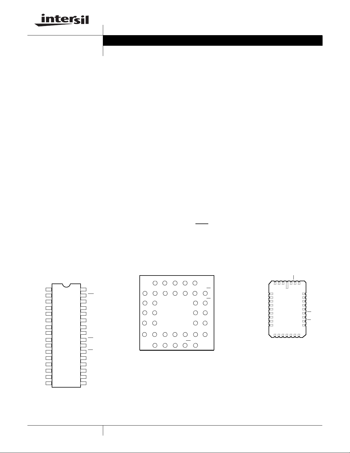
Pinouts
NC
A
16
A
15
A
12
A
7
A
6
A
5
A
4
A
3
A
2
A
1
A
0
I/O
0
I/O
1
I/O
2
V
SS
CERDIP
Flat Pack
SOIC (R)
1
2
3
4
5
6
7
8
X28C010
9
10
11
12
13
14
15
16
PGA
I/O
I/O
I/O
I/O
0
2
15
17
19
V
32
CC
WE
31
30
NC
29
A
14
28
A
13
27
A
8
26
A
9
25
A
11
24
OE
23
A
10
22
CE
21
I/O
I/O
I/O
I/O
I/O
7
6
5
4
3
20
19
18
17
A
I/O
A
0
1
14
13
A
A
3
2
11
12
A
A
5
4
9
10
A
A
7
6
7
8
A
A
12
15
6
5
A
16
4
V
1
SS
16
18
X28C010
(Bottom View)
V
CC
2NC36
3NC1NC35
I/O
3
5
6
21
22
I/O
20
NC
34
WE
CE
I/O
4
7
23
24
OE
A
10
26
25
A
A
9
11
28
27
A
A
13
8
30
29
A
NC
14
31
32
NC
33
EXTENDED LCC
12
A
A
A
5
7
A
6
6
A
7
5
A
8
4
X28C010
A
9
3
(Top View)
A
10
2
A
11
1
A
12
0
13
I/O
0
15 1716 18 19 2014
1
I/O
15
16
A
NC
23243 31
1
2
3
SS
I/O
I/O
V
CC
NC
V
WE
30
A
29
14
A
28
13
A
27
8
A
26
9
A
25
11
OE
24
A
23
10
CE
22
21
I/O
7
4
5
6
I/O
I/O
I/O
1
CAUTION: These devices are sensitive to electrostatic discharge; follow proper IC Handling Procedures.
1-888-INTERSIL or 1-888-468-3774
| Intersil (and design) is a registered trademark of Intersil Americas Inc.
All other trademarks mentioned are the property of their respective owners.
Copyright Intersil Americas Inc. 2005, 2007. All Rights Reserved

Ordering Information
www.BDTIC.com/Intersil
X28C010, X28HT010
ACCESS
PART NUMBER PART MARKING
X28C010D-12 X28C010D-12 120ns 0 to +70 32-Ld Cerdip F32.6
X28C010D-15 X28C010D-15 150ns 0 to +70 32-Ld Cerdip F32.6
X28C010DI X28C010DI - -40 to +85 32-Ld Cerdip F32.6
X28C010DI-12 X28C010DI-12 120ns -40 to +85 32-Ld Cerdip F32.6
X28C010DI-15 X28C010DI-15 150ns -40 to +85 32-Ld Cerdip F32.6
X28C010DM X28C010DM - -55 to +125 32-Ld Cerdip F32.6
X28C010DM-12 X28C010DM-12 120ns -55 to +125 32-Ld Cerdip F32.6
X28C010DM-15 X28C010DM-15 150ns -55 to +125 32-Ld Cerdip F32.6
X28C010DMB-12 C X28C010DMB-12 120ns MIL-STD-883 32-Ld Cerdip F32.6
X28C010DMB-15 C X28C010DMB-15 150ns MIL-STD-883 32-Ld Cerdip F32.6
X28C010DMB-20 C X28C010DMB-20 200ns MIL-STD-883 32-Ld Cerdip
X28C010FI-12 X28C010FI-12 120ns -40 to +85 32-Ld Flat Pack
X28C010FI-15 X28C010FI-15 150ns -40 to +85 32-Ld Flat Pack
X28C010FI-20 X28C010FI-20 200ns -40 to +85 32-Ld Flat Pack
X28C010FM X28C010FM - -55 to +125 32-Ld Flat Pack
X28C010FM-12 X28C010FM-12 120ns -55 to +125 32-Ld Flat Pack
X28C010FMB-12 C X28C010FMB-12 120ns MIL-STD-883 32-Ld Flat Pack
X28C010FMB-15 C X28C010FMB-15 150ns MIL-STD-883 32-Ld Flat Pack
X28C010K-25 X28C010K-25 250ns 0 to +70 36-Ld Pin Grid Array G36.760x760A
X28C010KM-12 X28C010KM-12 120ns -55 to +125 36-Ld Pin Grid Array G36.760x760A
X28C010KM-25 X28C010KM-25 250ns -55 to +125 36-Ld Pin Grid Array G36.760x760A
X28C010KMB-12 C X28C010KMB-12 120ns MIL-STD-883 36-Ld Pin Grid Array G36.760x760A
X28C010KMB-15 C X28C010KMB-15 150ns MIL-STD-883 36-Ld Pin Grid Array G36.760x760A
X28C010NM-12 X28C010NM-12 120ns -55 to +125 32-Ld Extended LCC
X28C010NM-15 X28C010NM-15 150ns -55 to +125 32-Ld Extended LCC
X28C010NMB-12 C X28C010NMB-12 120ns MIL-STD-883 32-Ld Extended LCC
X28C010NMB-15 C X28C010NMB-15 150ns MIL-STD-883 32-Ld Extended LCC
X28C010RI-12 X28C010RI-12 120ns -40 to +85 32-Ld Ceramic SOIC (Gull Wing)
X28C010RI-20 X28C010RI-20 200ns -40 to +85 32-Ld Ceramic SOIC (Gull Wing)
X28C010RI-20T1 X28C010RI-20 200ns -40 to +85 32-Ld Ceramic SOIC (Gull Wing)
X28C010RM-15 X28C010RM-15 150ns -55 to +125 32-Ld Ceramic SOIC (Gull Wing)
X28C010RMB-25 C X28C010RMB-25 250ns MIL-STD-883 32-Ld Ceramic SOIC (Gull Wing)
X28HT010W 200ns -40 to +175 Wafer
TIME
TEMP RANGE
(°C) PACKAGE PKG. DWG #
2
FN8105.1
February 12, 2007
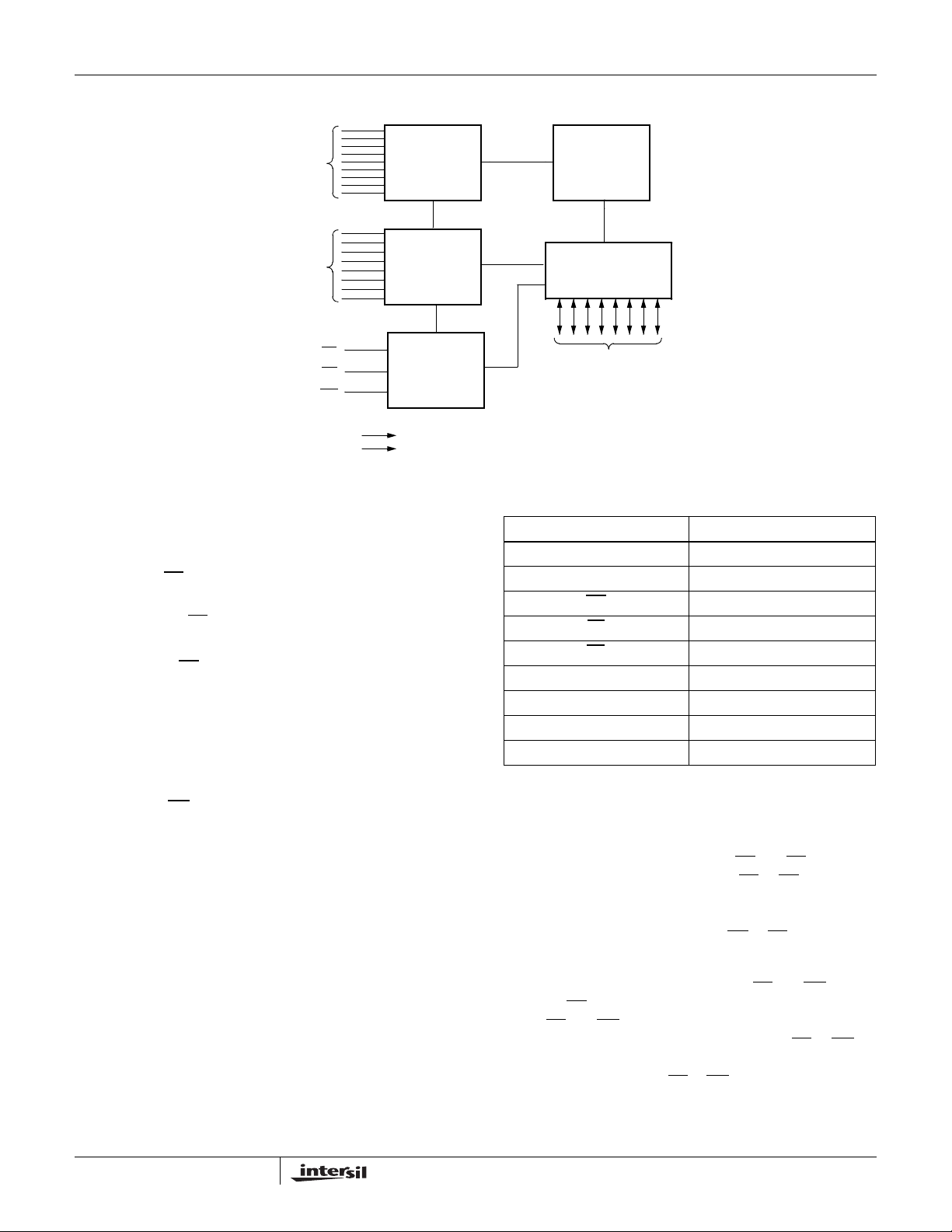
Block Diagram
www.BDTIC.com/Intersil
X28C010, X28HT010
X Buffers
A
8-A16
A0-A
7
V
V
CE
OE
WE
CC
SS
Latches and
Decoder
Y Buffers
Latches and
Decoder
Control
Logic and
Timing
Pin Descriptions
Addresses (A0-A16)
The Address inputs select an 8-bit memory location during a
read or write operation.
Chip Enable (CE)
The Chip Enable input must be LOW to enable all read/write
operations. When CE
reduced.
Output Enable (OE
The Output Enable input controls the d ata output buffers,
and is used to initiate read operations.
Data In/Data Out (I/O0-I/O7)
Data is written to or read from the X28C010/X28HT010
through the I/O pins.
is HIGH, power consumption is
)
1Mbit
EEPROM
Array
I/O Buffers
and Latches
I/O0-I/O
Data Inputs/Outputs
Pin Names
SYMBOL DESCRIPTION
A0-A
16
-I/O
I/O
0
WE
CE Chip Enable
OE
V
CC
V
SS
NC No Connect
*-3V
V
BB
applies to X28HT010 only.
*V
BB
7
Address Inputs
7
Data Input/Output
Write Enable
Output Enable
+5V
Ground
Write Enable (WE)
The Write Enable input controls the writing of data to the
X28C010/X28HT010.
Back Bias Voltage (VBB) (X28HT010 only)
It is required to provide -3V on pin 1. This negative voltage
improves higher temperature functionality.
Device Operation
Read
Read operations are initiated by both OE and CE LOW. The
read operation is terminated by either CE
HIGH. This two line control architecture eliminates bus
contention in a system environment. The data bus will be in
a high impedance state when either OE
Write
Write operations are initiated when both CE and WE are
LOW and OE
both a CE
and WE controlled write cycle. That is, the
address is latched by the falling edge of either CE
whichever occurs last. Similarly, the data is latched internally
by the rising edge of either CE
A byte write operation, once initiated, will automatically
continue to completion, typically within 5ms.
3
or OE returning
or CE is HIGH.
is HIGH. The X28C010/X28HT010 supports
or WE,
or WE, whichever occurs first.
FN8105.1
February 12, 2007
X28C010, X28HT010
www.BDTIC.com/Intersil
Page Write Operation
The page write feature of the X28C010/X28HT010 allows
the entire memory to be written in 5 seconds. Page write
allows two to two hundred fifty-six bytes of data to be
consecutively written to the X28C010/X28HT010 prior to the
commencement of the internal programming cycle. The host
can fetch data from another device within the system during
a page write operation (change the source address), but the
page address (A
write cycle to the part during this operation must be the same
as the initial page address.
The page write mode can be initiated during any write
operation. Following the initial byte write cycle, the host can
write an additional one to two hundred fifty six bytes in the
same manner as the first byte was written. Each successive
byte load cycle, started by the WE
must begin within 100µs of the falling edge of the preceding
WE
. If a subsequent WE HIGH to LOW transition is not
detected within 100µs, the internal automatic programming
cycle will commence. There is no page write window
limitation. Effectively the page write window is infinitely wide,
so long as the host continues to access the device within the
byte load cycle time of 100µs.
Write Operation Status Bits
The X28C010/X28HT010 provides the user two write
operation status bits. These can be used to optimize a
system write cycle time. The status bits are mapped onto the
I/O bus as shown in Figure 1.
through A16) for each subsequent valid
8
HIGH to LOW transition,
5TBDP 43210I/O
Reserved
Toggle Bit
DATA
Polling
FIGURE 1. STATUS BIT ASSIGNMENT
DATA Polling (I/O7)
The X28C010/X28HT010 features DATA Polling as a
method to indicate to the host system that the byte write or
page write cycle has completed. DATA
Polling allows a
simple bit test operation to determine the status of the
X28C010/X28HT010, eliminating additional interrupt inputs
or external hardware. During the internal programming cycle,
any attempt to read the last byte written will produce the
complement of that data on I/O
(i.e., write data = 0xxx xxxx,
7
read data = 1xxx xxxx). Once the programming cycle is
complete, I/O
will reflect true data. Note: If the
7
X28C010/X28HT010 is in the protected state, and an illegal
write operation is attempted, DATA
Polling will not operate.
Toggle Bit (I/O6)
The X28C010/X28HT010 also provides another method for
determining when the internal write cycle is complete. During
the internal programming cycle, I/O
LOW and LOW to HIGH on subsequent attempts to read the
device. When the internal cycle is complete the toggling will
cease and the device will be accessible for additional read or
write operations.
will toggle from HIGH to
6
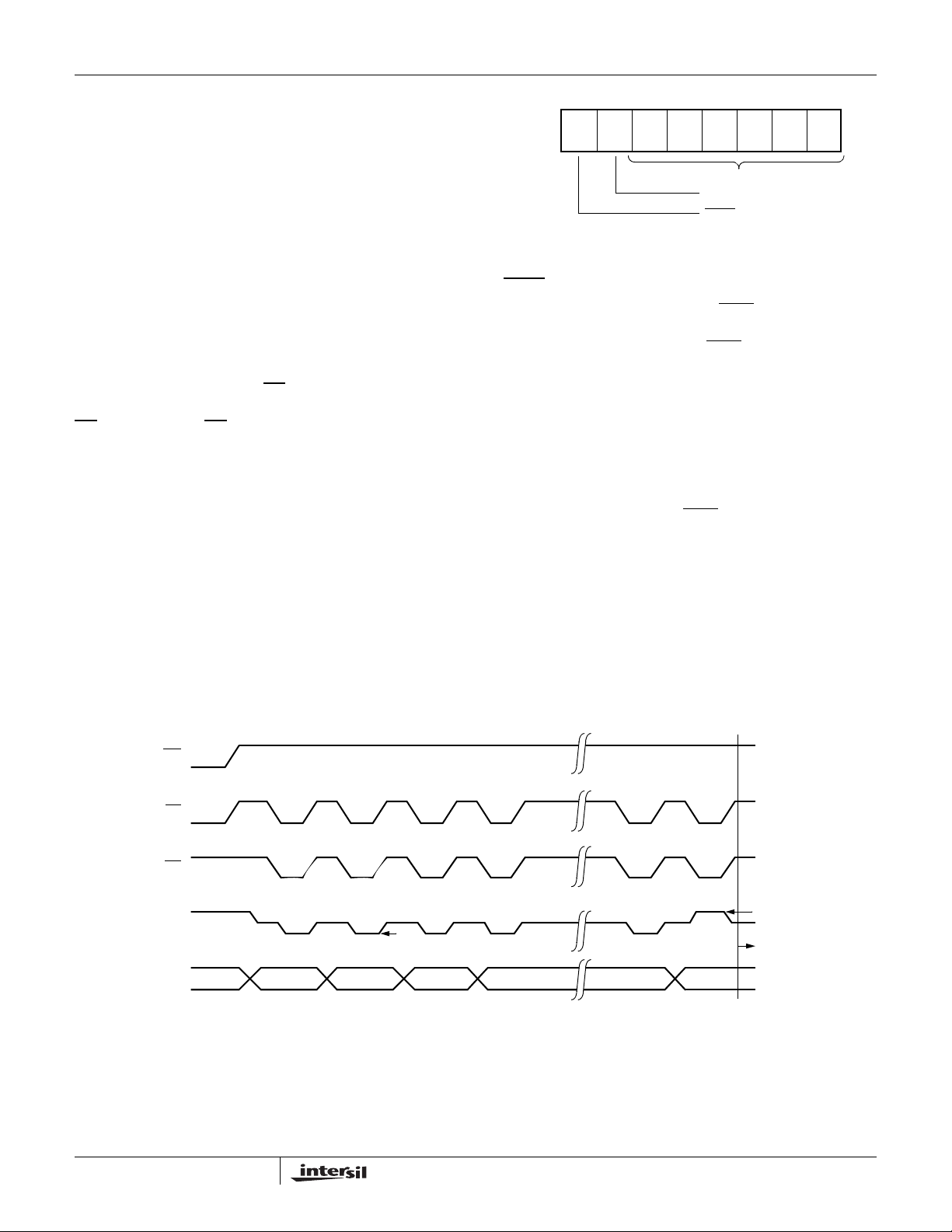
DATA Polling I/O
WE
CE
OE
I/O
7
A0-A
14
7
Last
Write
V
A
IH
n
HIGH Z
V
OL
A
n
A
n
FIGURE 2. DATA POLLING BUS SEQUENCE
A
n
A
n
A
n
V
OH
X28C010
Ready
A
n
4
FN8105.1
February 12, 2007
Write Data
www.BDTIC.com/Intersil
X28C010, X28HT010
DATA Polling can effectively halve the time for writing to the
X28C010/X28HT010. The timing diagram in Figure 2
illustrates the sequence of events on the bus. The software
flow diagram in Figure 3 illustrates one method of
implementing the routine.
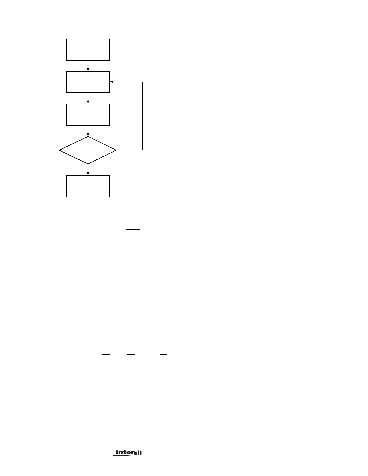
Writes
Complete?
Yes
Save Last Data
and Address
Read Last
Address
IO
7
Compare?
Yes
X28C010
Ready
No
No
FIGURE 3. DATA POLLING SOFTWARE FLOW
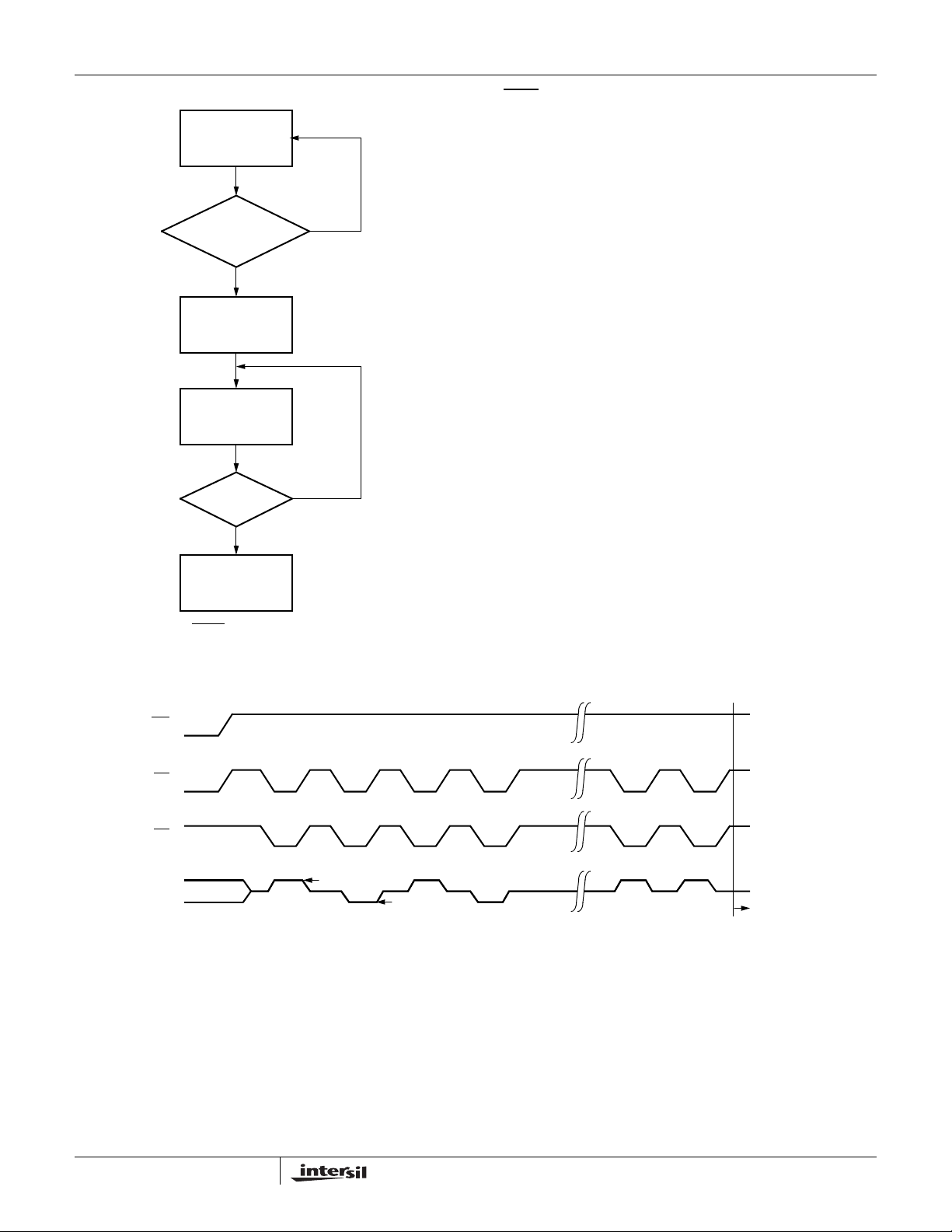
The Toggle Bit I/O
Last
Write
WE
CE
OE
I/O
6
6
V
OH
*
V
OL
* Beginning and ending state of I/O6 will vary
HIGH Z
*
X28C010
Ready
FIGURE 4. TOGGLE BIT BUS SEQUENCE
5
FN8105.1
February 12, 2007
Last Write
www.BDTIC.com/Intersil
Load Accum
From Addr N
Compare
Accum with
Addr N
Compare
Ok?
No
X28C010, X28HT010
Software Data Protection
The X28C010/X28HT010 offers a software controlled data
protection feature. The X28C010/X28HT010 is shipped from
Intersil with the software data protection NOT ENABLED:
that is the device will be in the standard operating mode. In
this mode data should be protected during power-up/-down
operations through the use of external circuits. The host
would then have open read and write access of the device
once V
CC
The X28C010/X28HT010 can be automatically protected
during power-up and power-down without the need for
external circuits by employing the software data protection
feature. The internal software data protection circuit is
enabled after the first write operation utilizing the software
algorithm. This circuit is nonvolatile and will remain set for
the life of the device unless the reset command is issued.
was stable.
Yes
Ready
FIGURE 5. TOGGLE BIT SOFTWARE FLOW
The Toggle Bit can eliminate the soft w are housekeeping
chore of saving and fetching the last address and data
written to a device in order to implement DATA
can be especially helpful in an array comprised of multiple
X28C010/X28HT010 memories that is frequently updated.
Toggle Bit Polling can also provide a method for status
checking in multiprocessor applications. The timing diagram
in Figure 4 illustrates the sequence of events on the bus.
The software flow diagram in Figure 5 illustrates a method
for polling the Toggle Bit.
Polling. This
Hardware Data Protection
The X28C010/X28HT010 provides three hardware features
that protect nonvolatile data from inadvertent writes.
• Noise Protection—A WE
initiate a write cycle.
pulse less than 10ns will not
Once the software protection is enabled, the
X28C010/X28HT010 is also protected from inadvertent and
accidental writes in the powered-up state. That is, the
software algorithm must be issued prior to writing additional
data to the device.
Software Algorithm
Selecting the software data protection mode requires the
host system to precede data write operations by a series of
three write operations to three specific addresses. Refer to
Figures 6 and 7 for the sequence. The three byte sequence
opens the page write window enabling the host to write from
one to two hundred fifty-six bytes of data. Once the page
load cycle has been completed, the device will automatically
be returned to the data protected state.
• Default V
is ≤ 3.5V.
• Write inhibit—Holding either OE
HIGH will prevent an inadvertent write cycle during powerup and power-down, maintaining data integrity.
Sense—All functions are inhibited when VCC
CC
LOW, WE HIGH, or CE
6
FN8105.1
February 12, 2007

Software Data Protection
www.BDTIC.com/Intersil
X28C010, X28HT010
V
CC
0V
CE
WE
Data
Addr
Write Data AA
to Address
5555
Write Data 55
to Address
2AAA
Write Data A0
to Address
5555
AA
5555
55
2AAA
FIGURE 6. TIMING SEQUENCE—BYTE OR PAGE WRITE
A0
5555
≤ t
BLC MAX
Writes
Regardless of whether the device has previously been
protected or not, once the software data protection algorithm
is used and data has been written, the X28C010/X28HT010
will automatically disable further writes unless another
command is issued to cancel it. If no further commands are
issued the X28C010/X28HT010 will be write protected
during power-down and after any subsequent power-up. The
state of A
care.
Note: Once initiated, the sequence of write operations
should not be interrupted.
(VCC)
t
WC
Ok
Byte
or
Page
and A16 while executing the algorithm is don’t
15
Write
Protected
Write Data XX
to Any
Address
Write Last
Byte
Last Address
After t
Re-Enters Data
Protected State
FIGURE 7. WRITE SEQUENCE FOR SOFTWARE DATA
PROTECTION
WC
Optional
Byte/Page
Load Operation
7
FN8105.1
February 12, 2007

Resetting Software Data Protection
www.BDTIC.com/Intersil
V
CC
X28C010, X28HT010
Data
AddrAA5555
CE
WE
FIGURE 8. RESET SOFTWARE DATA PROTECTION TIMING SEQUENCE
Write Data AA
to Address
5555
Write Data 55
to Address
2AAA
Write Data 80
to Address
5555
Write Data AA
to Address
5555
Write Data 55
to Address
2AAA
Write Data 20
to Address
5555
FIGURE 9. SOFTWARE SEQUENCE T O DEACTIV A TE
SOFTWARE DATA PROTECTION
55
2AAA
80
5555
In the event the user wants to deactivate the software data
protection feature for testing or reprogramming in an
EEPROM programmer, the following six step algorithm will
reset the internal protection circuit. After t
WC
, the
X28C010/X28HT010 will be in standard operating mode.
AA
5555
55
2AAA
20
5555
≥ t
WC
Standard
Operating
Mode
System Considerations
Because the X28C010/X28HT010 is frequently used in large
memory arrays, it is provided with a two line control
architecture for both read and write operations. Proper
usage can provide the lowest possible power dissipation and
eliminate the possibility of contention where multiple I/O pins
share the same bus.
To gain the most benefit, it is recommended that CE
decoded from the address bus and be used as the primary
device selection input. Both OE
and WE would then be
common among all devices in the array. For a read operation
this assures that all deselected devices are in their standby
mode and that only the selected device(s) is outputting data
on the bus.
Because the X28C010/X28HT010 has two power modes,
standby and active, proper decoupling of the memory array
is of prime concern. Enabling CE
will cause transient current
spikes. The magnitude of these spikes is dependent on the
output capacitive loading of the I/Os. Therefore, the larger
the array sharing a common bus, the larger the transient
spikes. The voltage peaks associated with the current
transients can be suppressed by the proper selection and
placement of decoupling capacitors. As a minimum, it is
recommended that a 0.1µF high frequency ceramic
capacitor be used between V
and VSS at each device.
CC
Depending on the size of the array, the value of the capacitor
may have to be larger.
In addition, it is recommended that a 4.7µF electrolytic bulk
capacitor be placed between V
CC
and V
for each eight
SS
devices employed in the array. This bulk capacitor is
employed to overcome the voltage droop caused by the
inductive effects of the PC board traces.
be
Note: Once initiated, the sequence of write operations
should not be interrupted.
8
FN8105.1
February 12, 2007

X28C010, X28HT010
www.BDTIC.com/Intersil
Active Supply Current vs. Ambient Temperature
18
16
14
WR (mA)
CC
I
12
V
= 5V
CC
10
-55 -10 +125
Ambient Temperature (°C)
+35 +80
Standby Supply Current vs. Ambient Temperature
0.3
0.25
0.2
(mA)
SB
I
0.15
0.1
0.05
-55 -10 +125
Ambient Temperature (°C)
(RD) by Temperature Over Frequency
I
CC
60
50
40
RD (mA)
30
CC
I
20
+35 +80
VCC = 5V
5.0 V
-55°C
+25°C
+125°C
CC
10
03 15
69
Frequency (MHz)
12
9
FN8105.1
February 12, 2007

X28C010, X28HT010
www.BDTIC.com/Intersil
Absolute Maximum Ratings Recommended Operating Conditions
Temperature under bias
X28C010 . . . . . . . . . . . . . . . . . . . . . . . . . . . . . . . .-10°C to +85°C
X28C010I . . . . . . . . . . . . . . . . . . . . . . . . . . . . . . .-65°C to +135°C
X28C010M . . . . . . . . . . . . . . . . . . . . . . . . . . . . . .-65°C to +135°C
X28HT010 . . . . . . . . . . . . . . . . . . . . . . . . . . . . . .-55°C to +175°C
Storage temperature . . . . . . . . . . . . . . . . . . . . . . . .-65°C to +150°C
Voltage on any pin with respect to V
D.C. output current. . . . . . . . . . . . . . . . . . . . . . . . . . . . . . . . . . . 5mA
Lead temperature
(soldering, 10 seconds) . . . . . . . . . . . . . . . . . . . . . . . . . . . . .+300°C
CAUTION: Stresses above those listed under “Absolute Maximum Ratings” may cause permanent damage to the device. This is a stress rating only; functional operation of
the device at these or any other conditions (ab ove those indicated in the operational sectio ns of this specification) is not implied. Exposure to absolute maximum rating
conditions for extended periods may affect device reliability.
. . . . . . . . . . . . . . -1V to +7V
SS
DC Electrical Specifications Over the recommended operating conditions, unless otherwise specified.
SYMBOL PARAMETER TEST CONDITIONS MIN MAX UNIT
I
CC
I
SB1
I
SB2
I
I
LO
(Note 1) Input LOW Voltage -1 0.8 V
V
lL
(Note 1) Input HIGH Voltage 2VCC + 1 V
V
IH
V
V
I
BB
NOTE:
1. V
IL
2. X28HT010W
VCC Current (Active) (TTL Inputs) CE = OE = VIL, WE = VIH, All I/O’s = Open,
Address Inputs = 0.4V/2.4V Levels @ f = 5MHz
VCC Current (Standby) (TTL Inputs) CE = VIH, OE = VIL, All I/O’s = Open, Other Inputs = V
VCC Current (Standby) (CMOS
Inputs)
Input Leakage Current VIN = V
LI
Output Leakage Current V
Output LOW Voltage IOL = 2.1mA 0.4 V
OL
Output HIGH Voltage IOH = -400µA 2.4 V
OH
Back Bias Current VBB = -3V ±10% (Note 2) 200 µA
min. and VIH max. are for reference only and are not tested.
CE = VCC - 0.3V, OE = VIL, All I/O’s = Open,
Other Inputs = V
SS
= V
V
IN
SS
= VSS to VCC, CE = V
OUT
= VSS to VCC, CE = VIH (Note 2) 20 µA
V
OUT
(Note 2) -1 0.6 V
(Note 2) 2.2 V
= 1mA (Note 2) 0.5 V
I
OL
= -400µA 2.6 V
I
OH
CC
to V
CC
to VCC (Note 2) 20 µA
Commercial . . . . . . . . . . . . . . . . . . . . . . . . . . . . . . . . . 0°C to +70°C
Industrial . . . . . . . . . . . . . . . . . . . . . . . . . . . . . . . . . .-40°C tp +85°C
Military . . . . . . . . . . . . . . . . . . . . . . . . . . . . . . . . . . .-55°C to +125°C
Supply Voltage. . . . . . . . . . . . . . . . . . . . . . . . . . . . . . . . . . .5V ±10%
High Temperature . . . . . . . . . . . . . . . . . . . . . . . . . .-40°C to +175°C
50 mA
IH
IH
3mA
500 µA
10 µA
10 µA
+ 1 V
CC
Power-Up Timing
SYMBOL PARAMETER MAX UNIT
(Note 3) Power-up to Read operation 100 µs
t
PUR
(Note 3) Power-up to Write operation 5 ms
t
PUW
Capacitance T
SYMBOL PARAMETER TEST CONDITIONS MAX UNIT
(Note 3) Input/Output capacitance V
C
I/O
(Note 3) Input capacitance V
C
IN
NOTE:
3. This parameter is periodically sampled and not 100% tested.
= +25°C, f = 1MHz, VCC = 5V
A
10
= 0V 10 pF
I/O
= 0V 10 pF
IN
February 12, 2007
FN8105.1

X28C010, X28HT010
www.BDTIC.com/Intersil
Endurance and Data Retention
PARAMETER MIN MAX UNIT
Endurance 10,000 Cycles per byte
Endurance 100,000 Cycles per page
Data Retention 100 Years
A.C. Conditions of Test
Input pulse levels 0V to 3V
Input rise and fall times 10ns
Input and output timing levels 1.5V
Mode Selection
CE OE WE MODE I/O POWER
LLH Read D
LHL Write D
H X X Standby and
Write Inhibit
X L X Write Inhibit — —
X X H Write Inhibit — —
OUT
IN
High Z Standby
Equivalent A.C. Load Circuit
5V
1.92kΩ
Output
Active
Active
Symbol Table
WAVEFORM INPUTS OUTPUTS
Must be
steady
May change
from LOW
to HIGH
May change
from HIGH
to LOW
Don’t Care:
Changes
Allowed
N/A Center Line
Will be
steady
Will change
from LOW
to HIGH
Will change
from HIGH
to LOW
Changing:
State Not
Known
is High
Impedance
1.37kΩ
100pF
AC Electrical Specifications Over the recommended operating conditions, unless otherwise specified.
X28C010-12 X28C010-15
SYMBOL PARAMETER
READ CYCLE LIMITS
t
RC
t
CE
t
AA
t
OE
(Note 4) CE
t
LZ
(Note 4) OE LOW to active output 0 0 0 0 ns
t
OLZ
(Note 4) CE HIGH to high Z output 50 50 50 50 ns
t
HZ
(Note 4) OE HIGH to high Z output 50 50 50 50 ns
t
OHZ
t
OH
Read cycle time 120 150 200 250 ns
Chip enable access time 120 150 200 250 ns
Address access time 120 150 200 250 ns
Output enable access time 50 50 50 50 ns
LOW to active output 0 0 0 0 ns
Output hold from address change 0 0 0 0 ns
X28C010-20,
X28HT010W X28C010-25
UNITMIN MAX MIN MAX MIN MAX MIN MAX
11
FN8105.1
February 12, 2007

Read Cycle
www.BDTIC.com/Intersil
Address
CE
OE
WE
Data I/O
NOTE:
min.,tHZ, t
4. t
LZ
when CE
X28C010, X28HT010
t
RC
t
CE
t
OE
V
IH
t
OLZ
t
LZ
HIGH Z
min., and t
OLZ
are periodically sampled and not 100% tested. tHZ max. and t
OHZ
Data Valid
or OE return HIGH (whichever occurs first) to the time when the outputs are no longer driven.
t
OH
t
AA
max. are measured, with CL = 5pF , from the point
OHZ
Data Valid
t
OHZ
t
HZ
Write Cycle Limits
SYMBOL PARAMETER MIN MAX UNIT
(Note 5) Write cycle time 10 ms
t
WC
t
AS
t
AH
t
CS
t
CH
t
CW
t
OES
t
OEH
t
WP
t
WPH
t
DV
t
DS
t
DH
t
DW
t
BLC
Address setup time 0 ns
Address hold time 50 ns
Write setup time 0 ns
Write hold time 0 ns
CE pulse width 100 ns
OE HIGH setup time 10 ns
OE HIGH hold time 10 ns
WE pulse width 100 ns
WE HIGH recovery 100 ns
Data valid 1µs
Data setup 50 ns
Data hold 0 ns
Delay to next write 10 µs
Byte load cycle 0.2 100 µs
12
FN8105.1
February 12, 2007

WE Controlled Write Cycl e
www.BDTIC.com/Intersil
Address
CE
OE
WE
X28C010, X28HT010
t
WC
t
AS
t
CS
t
OES
t
DV
t
AH
t
CH
t
t
WP
OEH
t
WPH
t
DS
Data Valid
HIGH Z
t
DH
Data In
Data Out
NOTE:
is the minimum cycle time to be allowed from the system perspective unless polling techniques are used. It is the maximum time the device
5. t
WC
requires to complete internal write operation.
CE Controlled Write Cycle
t
WC
Address
CE
OE
WE
Data In
Data Out
t
OES
t
AS
t
CS
t
DV
t
AH
t
CW
t
WPH
t
OEH
t
CH
Data Valid
t
DS
HIGH Z
t
DH
13
FN8105.1
February 12, 2007

Page Write Cycle
www.BDTIC.com/Intersil
(Note 5)
OE
CE
X28C010, X28HT010
t
BLC
should be the same or
16
Last Byte
t
WC
WE
Address*
(Note 7)
I/O
t
WP
t
WPH
Byte 0 Byte 1 Byte 2 Byte n Byte n+1 Byte n+2
*For each successive write within the page write operation, A8-A
writes to an unknown address could occur.
NOTES:
6. Between successive byte writes within a page write operation, OE
data from another memory device within the system for the next write; or with WE
can be strobed LOW: e.g. this can be done with CE and WE HIGH to fetch
HIGH and CE LOW effectively performing a polling operation.
7. The timings shown above are unique to page write operations. Individual byte load operations within the page write must conform to either the
or WE controlled write cycle timing.
CE
DATA Polling Timing Diagram (Note 8)
Address A
n
A
n
A
n
WE
I/O
CE
OE
t
OEH
7
DIN = X
D
= X D
OUT
t
WC
OUT
t
DW
= X
t
OES
14
FN8105.1
February 12, 2007

X28C010, X28HT010
www.BDTIC.com/Intersil
Toggle Bit Timing Diagram
CE
WE
t
OEH
OE
I/O
6
NOTE:
8. Polling operations are by definition read cycles and are therefore subject to read cycle timings.
HIGH Z
*
t
WC
beginning and ending state will vary.
* I/O
6
t
OES
t
DW
*
15
FN8105.1
February 12, 2007

X28C010, X28HT010
www.BDTIC.com/Intersil
Ceramic Dual-In-Line Frit Seal Packages (CERDIP)
LEAD FINISH
c1
-A-
-B-
bbb C A - B
S
BASE
PLANE
SEATING
PLANE
S1
b2
b
ccc C A - BMD
D
A
A
e
S
S
NOTES:
1. Index area: A notch or a pin one identification mark shall be located adjacent to pin one and shall be located within the shaded
area shown. The manufacturer’s identification shall not be used
as a pin one identification mark.
2. The maximum limits of lead dimensions b and c or M shall be
measured at the centroid of the finished lead surfaces, when
solder dip or tin plate lead finish is applied.
3. Dimensions b1 and c1 apply to lead base metal only. Dimension
M applies to lead plating and finish thickness.
4. Corner leads (1, N, N/2, and N/2+1) may be configured with a
partial lead paddle. For this configuration dimension b3 replaces
dimension b2.
5. This dimension allows for off-center lid, meniscus, and glass
overrun.
6. Dimension Q shall be measured from the seating plane to the
base plane.
7. Measure dimension S1 at all four corners.
8. N is the maximum number of terminal positions.
9. Dimensioning and tolerancing per ANSI Y14.5M - 1982.
10. Controlling dimension: INCH.
-D-
BASE
E
D
S
S
Q
A
-C-
L
METAL
b1
M
(b)
SECTION A-A
α
(c)
M
eA
eA/2
aaa CA - B
M
c
D
S
S
F32.6 MIL-STD-1835 GDIP1-T32 (D-16, CONFIGURATION A)
32 LEAD CERAMIC DUAL-IN-LINE FRIT SEAL PACKAGE
INCHES MILLIMETERS
SYMBOL
A - 0.232 - 5.92 -
b 0.014 0.026 0.36 0.66 2
b1 0.014 0.023 0.36 0.58 3
b2 0.045 0.065 1.14 1.65 -
b3 0.023 0.045 0.58 1.14 4
c 0.008 0.018 0.20 0.46 2
c1 0.008 0.015 0.20 0.38 3
D - 1.690 - 42.95 5
E 0.500 0.610 12.70 15.49 5
e 0.100 BSC 2.54 BSC -
eA 0.600 BSC 15.24 BSC -
eA/2 0.300 BSC 7.62 BSC -
L 0.125 0.200 3.18 5.08 -
Q 0.015 0.060 0.38 1.52 6
S1 0.005 - 0.13 - 7
α
90° 105° 90° 105° -
aaa - 0.015 - 0.38 -
bbb - 0.030 - 0.76 -
ccc - 0.010 - 0.25 -
M - 0.0015 - 0.038 2, 3
N32 328
NOTESMIN MAX MIN MAX
Rev. 0 8/06
16
FN8105.1
February 12, 2007

Packaging Information
www.BDTIC.com/Intersil
0.830 (21.08) Max.
X28C010, X28HT010
32-Lead Ceramic Flat Pack Type F
1.228 (31.19)
1.000 (25.40)
Pin 1 Index
132
0.019 (0.48)
0.015 (0.38)
0.050 (1.27) BSC
0.045 (1.14) Max.
0.007 (0.18)
0.004 (0.10)
0.370 (9.40)
0.270 (6.86)
0.030 (0.76)
Min.
NOTE: ALL DIMENSIONS IN INCHES (IN PARENTHESES IN MILLIMETERS)
0.440
0.430 (10.93)
0.347 (8.82)
0.330 (8.38)
0.005 (0.13) Min.
0.120 (3.05)
0.090 (2.29)
0.026 (0.66)
Min.
17
FN8105.1
February 12, 2007

Packaging Information
www.BDTIC.com/Intersil
32-Pad Stretched Ceramic Leadless Chip Carrier Package Type N
0.400 BSC
Pin 1
0.300 BSC
0.050 BSC
X28C010, X28HT010
0.035 x 45° Ref.
0.085 ± 0.010
Detail A
0.020 (1.02) x 45° Ref.
Typ. (3) Plcs.
0.025 ± 0.003
Detail A
0.005/0.015
0.006/0.022
0.050 ± 0.005
0.700 ± 0.010
0.450 ± 0.008
0.458 Max.
Pin #1 Index Corner
NOTES:
1. ALL DIMENSIONS IN INCHES (IN PARENTHESES IN MILLIMETERS)
2. TOLERANCE: ±1% NLT±0.005 (0.127)
0.060/0.120
0.708 Max.
18
FN8105.1
February 12, 2007

Packaging Information
www.BDTIC.com/Intersil
32-Lead Ceramic Small Outline Gull Wing Package Type R
0.340
±0.007
X28C010, X28HT010
See Detail “A”
For Lead
Information
0.165 Typ.
0.060 Nom.
0.020 Min.
0.015 R Typ.
0.830
Max.
0.019
0.015
0.050
0.440 Max.
0.560 Nom.
0.750
±0.005
0.035 Typ.
0.560"
Typical
FOOTPRINT
Detail “A”
0.050"
Typical
0.030" Typical
32 Places
0.015 R
Typ.
0.035 Min.
0.050"
Typical
NOTES:
1. ALL DIMENSIONS IN INCHES
2. FORMED LEAD SHALL BE PLANAR WITH RESPECT TO ONE ANOTHER WITHIN 0.004 INCHES
19
FN8105.1
February 12, 2007

Packaging Information
www.BDTIC.com/Intersil
X28C010, X28HT010
36 Lead Ceramic Pin Grid Array Package
Package Code G36.760x760A
Typ. 0.180 (.010)
(4.57 ± .25)
4 Corners
15 17 19 21 22
13
14 16 18 20 23
12 11 25 26
10 9 27
8 7 29 30
6 31
5 2 36 34 32
4 3 1 35 33
Typ. 0.180 (.010)
(4.57 ± .25)
4 Corners
Pin 1 Index
24
28
A
A
NOTE: Leads 5, 14, 23, & 32
Typ. 0.100 (2.54)
All Leads
0.008 (0.20)
0.050 (1.27)
0.120 (3.05)
0.100 (2.54)
0.072 (1.83)
0.062 (1.57)
0.770 (19.56)
0.750 (19.05)
SQ
A
A
NOTE: ALL DIMENSIONS IN INCHES (IN PARENTHESES IN MILLIMETERS)
0.020 (0.51)
0.016 (0.41)
0.185 (4.70)
0.175 (4.45)
All Intersil U.S. products are manufactured, assembled and tested utilizing ISO9000 quality systems.
Intersil Corporation’s quality certifications can be viewed at www.intersil.com/design/quality
Intersil products are sold by description only. Intersil Corporation reserves the right to make changes in circuit design, software and/or specifications at any time without
notice. Accordingly, the reader is cautioned to verify that data sheets are current before placing orders. Information furnished by Intersil is believed to be accurate and
reliable. However, no responsibility is assumed by Intersil or its subsidiaries for its use; nor for any infringements of patents or other rights of third parties which may result
from its use. No license is granted by implic atio n or other wise u nde r any p a tent or patent rights of Intersil or its subsidiaries.
For information regarding Intersil Corporation and its products, see www.intersil.com
20
FN8105.1
February 12, 2007
 Loading...