

®
www.BDTIC.com/Intersil
X28C512, X28C513
Data Sheet June 7, 2006
5V, Byte Alterable EEPROM
The X28C512, X28C513 are 64K x 8 EEPROM, fabricated
with Intersil’s proprietary, high performance, floating gate
CMOS technology. Like all Intersil programmable nonvolatile
memories, the X28C512, X28C513 are 5V only devices. The
X28C512, X28C513 feature the JEDEC approved pin out for
byte wide memories, compatible with industry standard
EPROMS.
The X28C512, X28C513 support a 128-byte page write
operation, effectively providing a 39µs/byte write cycle and
enabling the entire memory to be written in less than 2.5
seconds. The X28C512, X28C513 also feature DAT A
and Toggle Bit Polling, system software support schemes
used to indicate the early completion of a write cycle. In
addition, the X28C512, X28C513 support the software data
protection option.
Polling
FN8106.2
Features
• Access Time: 90ns
• Simple Byte and Page Write
- Single 5V supply
• No external high voltages or VPP control circuits
- Self-timed
• No erase before write
• No complex programming algorithms
• No overerase problem
• Low Power CMOS
- Active: 50mA
- Standby: 500µA
• Software Data Protection
- Protects data against system level inadvertent writes
• High Speed Page Write Capability
™
• Highly Reliable Direct Write
- Endurance: 100,000 write cycles
- Data retention: 100 years
- Early end of write detection
-DATA
- Toggle bit polling
polling
Cell
• Two PLCC and LCC Pinouts
- X28C512
• X28C010 EPROM pin compatible
- X28C513
• Compatible with lower density EEPROMs
• Pb-Free Plus Anneal Available (RoHS Compliant)
1
CAUTION: These devices are sensitive to electrostatic discharge; follow proper IC Handling Procedures.
1-888-INTERSIL or 1-888-468-3774
| Intersil (and design) is a registered trademark of Intersil Americas Inc.
All other trademarks mentioned are the property of their respective owners.
Copyright Intersil Americas Inc. 2005, 2006. All Rights Reserved
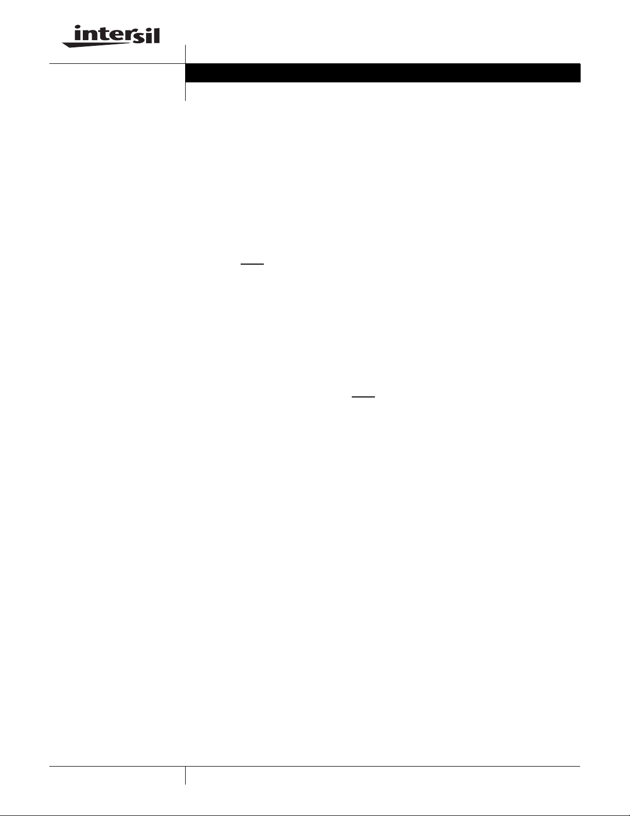
Block Diagram
www.BDTIC.com/Intersil
A7-A
X28C512, X28C513
512Kbit
X Buffers
15
Latches and
Decoder
EEPROM
Array
I/O Buffers
and Latches
I/O0-I/O
7
Data Inputs/Outputs
A0-A
6
V
V
CE
OE
WE
CC
SS
Y Buffers
Latches and
Decoder
Control
Logic and
Timing
Ordering Information
PART NUMBER PART MARKING
X28C512D X28C512D - 0 to +70 32 Ld CERDIP
X28C512DM X28C512DM -55 to +125 32 Ld CERDIP
X28C512J X28C512J 0 to +70 32 Ld PLCC
X28C513EM X28C513EM -55 to +125 32 Ld LCC
X28C512D-12 X28C512D-12 120 0 to +70 32 Ld CERDIP
X28C512DI-12 X28C512DI-12 -40 to +85 32 Ld CERDIP
X28C512DMB-12 X28C512DMB-12 Mil-STD-883 32 Ld CERDIP
X28C512FMB-12 X28C512FMB-12 Mil-STD-883 32 Ld Flat Pack
X28C512J-12* X28C512J-12 0 to +70 32 Ld PLCC
X28C512JZ-12* (See Note) X28C512J-12 Z 0 to +70 32 Ld PLCC (Pb-free)
X28C512JI-12 X28C512JI-12 -40 to +85 32 Ld PLCC
X28C512JIZ-12* (See Note) X28C512JI-12 Z -40 to +85 32 Ld PLCC (Pb-free)
X28C512JM-12 X28C512JM-12 -55 to +125 32 Ld PLCC
X28C512KM-12 X28C512KM-12 -55 to +125 36 Ld CPGA
X28C512PI-12 X28C512PI-12 -40 to +85 32 Ld PDIP
X28C512RMB-12 X28C512RMB-12 Mil-STD-883 32 Ld Flat Pack
X28C513EM-12 X28C513EM-12 -55 to +125 32 Ld LCC
X28C513EMB-12 X28C513EMB-12 Mil-STD-883 32 Ld LCC
X28C513J-12* X28C513J-12 0 to +70 32 Ld PLCC
X28C513JZ-12* (Note) X28C513J-12 Z 0 to +70 32 Ld PLCC (Pb-free)
X28C513JI-12* X28C513JI-12 -40 to +85 32 Ld PLCC
X28C513JIZ-12* (Note) X28C513JI-12 Z -40 to +85 32 Ld PLCC (Pb-free)
X28C513JM-12 X28C513JM-12 -55 to +125 32 Ld PLCC
ACCESS TIME
(ns) TEMP RANGE (°C) PACKAGE
2
FN8106.2
June 7, 2006
X28C512, X28C513
www.BDTIC.com/Intersil
Ordering Information (Continued)
ACCESS TIME
PART NUMBER PART MARKING
X28C512D-15 X28C512D-15 150 0 to +70 32 Ld CERDIP
X28C512DI-15 X28C512DI-15 -40 to +85 32 Ld CERDIP
X28C512DMB-15 X28C512DMB-15 Mil-STD-883 32 Ld CERDIP
X28C512J-15* X28C512J-15 0 to +70 32 Ld PLCC
X28C512JZ-15* (See Note) X28C512J-15 Z 0 to +70 32 Ld PLCC (Pb-free)
X28C512JI-15* X28C512JI-15 -40 to +85 32 Ld PLCC
X28C512JIZ-15* (See Note) X28C512JI-15 Z -40 to +85 32 Ld PLCC (Pb-free)
X28C512JM-15 X28C512JM-15 -55 to +125 32 Ld PLCC
X28C513EM-15 X28C513EM-15 -55 to +125 32 Ld LCC
X28C513EMB-15 X28C513EMB-15 Mil-STD-883 32 Ld LCC
X28C513J-15* X28C513J-15 0 to +70 32 Ld PLCC
X28C513JZ-15* (Note) X28C513J-15 Z 0 to +70 32 Ld PLCC (Pb-free)
X28C513JI-15 X28C513JI-15 -40 to +85 32 Ld PLCC
X28C513JIZ-15* (Note) X28C513JI-15 Z -40 to +85 32 Ld PLCC (Pb-free)
X28C513JM-15 X28C513JM-15 -55 to +125 32 Ld PLCC
X28C512DMB-20 X28C512DMB-20 200 Mil-STD-883 32 Ld CERDIP
X28C512JM-20 X28C512JM-20 -55 to +125 32 Ld PLCC
X28C512KI-20 X28C512KI-20 -40 to +85 36 Ld CPGA
X28C512KM-20 X28C512KM-20 -55 to +125 36 Ld CPGA
X28C513EI-20 X28C513EI-20 -40 to +85 32 Ld LCC
X28C513EM-20 X28C513EM-20 -55 to +125 32 Ld LCC
X28C513EMB-20 X28C513EMB-20 Mil-STD-883 32 Ld LCC
X28C513J-20T1 X28C513J-20 0 to +70 32 Ld PLCC Tape and Reel
X28C512EM-25 X28C512EM-25 250 -55 to +125 32 Ld LCC
X28C512JM-25 X28C512JM-25 -55 to +125 32 Ld PLCC
X28C512KM-25 X28C512KM-25 -55 to +125 36 Ld CPGA
X28C512KMB-25 X28C512KMB-25 Mil-STD-883 36 Ld CPGA
X28C513EM-25 X28C513EM-25 -55 to +125 32 Ld LCC
X28C513EMB-25 X28C513EMB-25 Mil-STD-883 32 Ld LCC
*Add "T1" suffix for tape and reel.
NOTE: Intersil Pb-free plus anneal p roducts e mploy special Pb-free mate rial sets; mold ing compounds/die att ach materials and 10 0% matte tin pla te termination fi nish,
which are RoHS compliant and compatible with both SnPb and Pb-free soldering ope rations. Intersil Pb-free products are MSL classified at Pb-free peak reflow
temperatures that meet or exceed the Pb-free requirements of IPC/JEDEC J STD-020.
(ns) TEMP RANGE (°C) PACKAGE
3
FN8106.2
June 7, 2006
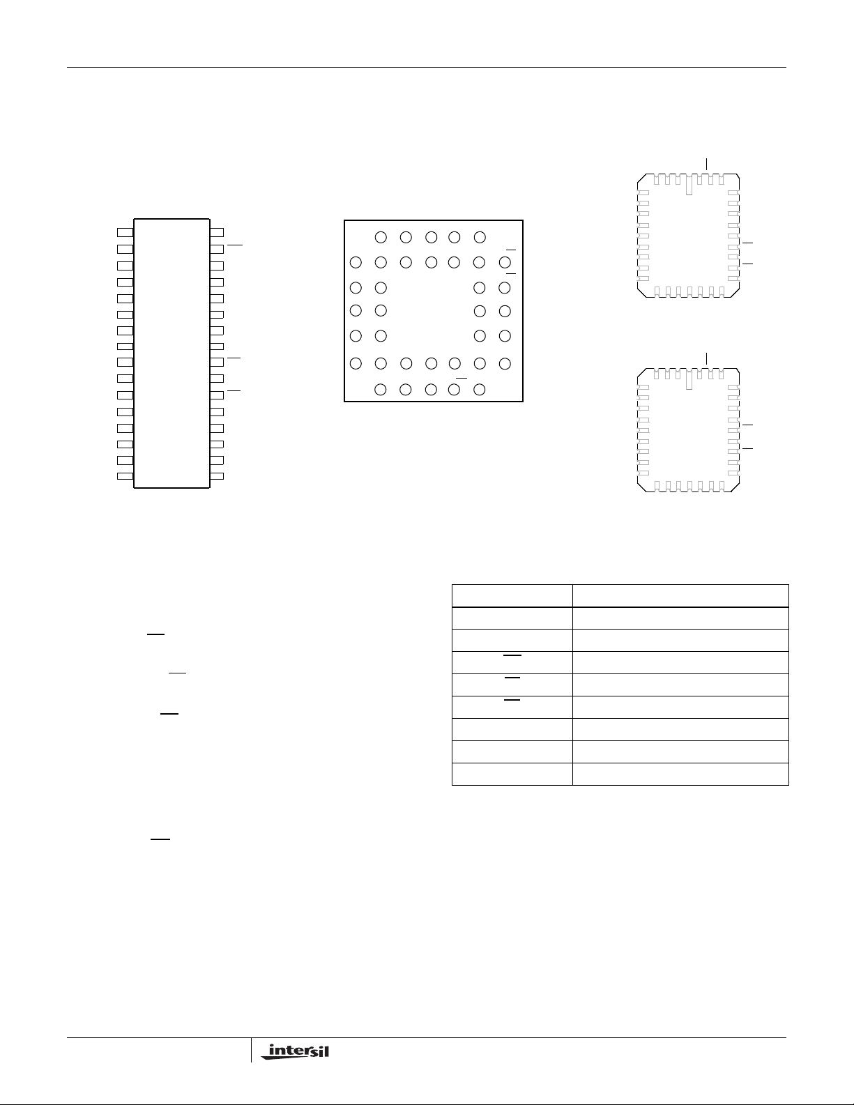
Pinouts
www.BDTIC.com/Intersil
NC
NC
A
15
A
12
A
7
A
6
A
5
A
4
A
3
A
2
A
1
A
0
I/O
0
I/O
1
I/O
2
V
SS
Plastic DIP
CERDIP
FLAT Pack
SOIC (R)
1
2
3
4
5
6
7
8
X28C512
9
10
11
12
13
14
15
16
32
31
30
29
28
27
26
25
24
23
22
21
20
19
18
17
V
WE
NC
A
A
A
A
A
OE
A
CE
I/O
I/O
I/O
I/O
I/O
CC
14
13
8
9
11
10
X28C512, X28C513
PLCC/LCC
12
A
A
NC
4 3
5
A7
A
6
PGA
I/O0
I/O2
I/O3
I/O
I/O6
15
17
A
A1
13
A
2
12
A
4
10
A
6
8
A
12
6
I/O
0
1
14
16
A
3
11
A
5
9
A
7
7
2 NC
A
15
5
NC 3 NC 1 NC
4
Bottom
5
4
3
2
1
19
VSS
18
View
VCC
36
5
21
I/O
4
20
NC
34
35 WE33
22
CE
I/O7
23
24
OE
A10
25
26
A
A
11
9
27
28
A8
A
13
29
30
NC
A14
32
31
NC
6
A
5
A
4
A3
A
2
A
1
A0
I/O
0
A6
A
5
A
4
A
3
A2
A
1
A
0
NC
I/O
0
7
8
X28C512
9
(Top View)
10
11
12
13
15 17 16 18 19 20
14
I/O1
I/O2VSSI/O3I/O4I/O5I/O
7
A
A
4 3
5
6
7
8
X28C513
9
(Top View)
10
11
12
13
15 17 16 18 19 20
14
I/O1
I/O2V
15
NC
VCC WE
2 32
1
12
VCC WE
A14A15A
2 32
1
SS
NC
I/O
3
31
31
29
28
27
26
25
24
23
22
29
28
27
26
25
24
23
22
I/O4I/O
NC
30
A14
A
13
A
8
A9
A
11
OE
A
10
CE
I/O
7
21
6
13
30
A
8
A
9
A
11
NC
OE
A
10
CE
I/O
7
I/O
6
21
5
Pin Descriptions
Addresses (A0-A15)
The Address inputs select an 8-bit memory location during a
read or write operation.
Chip Enable (CE)
The Chip Enable input must be LOW to enable all read/write
operations. When CE is HIGH, power consumption is
reduced.
Output Enable (OE
The Output Enable input controls the data output buffers and
is used to initiate read operations.
Data In/Data Out (I/O
Data is written to or read from the X28C512, X28C513
through the I/O pins.
Write Enable (WE)
The Write Enable input controls the writing of data to the
X28C512, X28C513.
)
-I/O7)
0
Pin Names
SYMBOL DESCRIPTION
A
0-A15
I/O0-I/O
7
WE
CE
OE
V
CC
V
SS
NC No Connect
Address Inputs
Data Input/Output
Write Enable
Chip Enable
Output Enable
+5V
Ground
4
FN8106.2
June 7, 2006
X28C512, X28C513
www.BDTIC.com/Intersil
Device Operation
Read
Read operations are initiated by both OE and CE LOW. The
read operation is terminated by either CE
HIGH. This two line control architecture eliminates bus
contention in a system environment. The data bus will be in
a high impedance state when either OE
Write
Write operations are initiated when both CE and WE are
LOW and OE
both a CE
address is latched by the falling edge of either CE
whichever occurs last. Similarly, the data is latched internally
by the rising edge of either CE
A byte write operation, once initiated, will automatically
continue to completion, typically within 5ms.
is HIGH. The X28C512, X28C513 support
and WE controlled write cycle. That is, the
or WE, whichever occurs first.
Page Write Operation
The page write feature of the X28C512, X28C513 allows the
entire memory to be written in 2.5 seconds. Page write
allows two to one hundred twenty-eight bytes of data to be
consecutively written to the X28C512, X28C513, prior to the
commencement of the internal programming cycle. The host
can fetch data from another device within the system during
a page write operation (change the source address), but the
page address (A
write cycle to the part during this operation must be the same
as the initial page address.
through A15) for each subsequent valid
7
or OE returning
or CE is HIGH.
or WE,
DATA Polling (I/O7)
The X28C512, X28C513 feature DATA polling as a method
to indicate to the host system that the byte write or page
write cycle has completed. DATA
test operation to determine the status of the X28C512,
X28C513, eliminating additional interrupt inputs or external
hardware. During the internal programming cycle, any
attempt to read the last byte written will produce the
complement of that data on I/O
read data = 1xxx xxxx). Once the programming cycle is
complete, I/O
will reflect true data.
7
Polling allows a simple bit
(i.e. write data = 0xxx xxxx,
7
Toggle Bit (I/O6)
The X28C512, X28C513 also provide another method for
determining when the internal write cycle is complete. During
the internal programming cycle, I/O
LOW and LOW to HIGH on subsequent attempts to read the
device. When the internal cycle is complete, the toggling will
cease, and the device will be accessible for additional read
or write operations.
will toggle from HIGH to
6
The page write mode can be initiated during any write
operation. Following the initial byte write cycle, the host can
write an additional one to one hundred twenty-seven bytes in
the same manner as the first byte was written. Each
successive byte load cycle, started by the WE
transition, must begin within 100µs of the falling edge of the
preceding WE
is not detected within 100µs, the internal automatic
programming cycle will commence. There is no page write
window limitation. Effectively, the page write window is
infinitely wide, so long as the host continues to access the
device within the byte load cycle time of 100µs.
. If a subsequent WE HIGH to LOW transition
HIGH to LOW
Write Operation Status Bits
The X28C512, X28C513 provide the user two write
operation status bits. These can be used to optimize a
system write cycle time. The status bits are mapped onto the
I/O bus as shown in Figure 1.
5TBDP 43210I/O
Reserved
Toggle Bit
DATA
Polling
FIGURE 1. STATUS BIT ASSIGNMENT
5
FN8106.2
June 7, 2006
X28C512, X28C513
www.BDTIC.com/Intersil
DATA Polling I/O
Last
Write
WE
CE
OE
V
IH
I/O
7
A0-A
A
15
n
Write Data
7
V
HIGH Z
V
OL
A
n
A
n
A
n
A
n
A
n
A
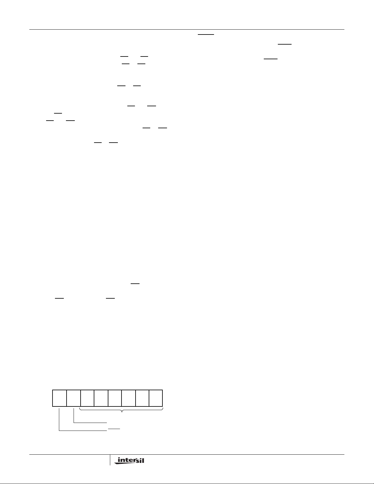
FIGURE 2A. DATA POLLING BUS SEQUENCE
DATA Polling can effectively halve the time for writing to the
X28C512, X28C513. The timing diagram in Figure 2A
illustrates the sequence of events on the bus. The software
flow diagram in Figure 2B illustrates one method of
implementing the routine.
OH
X28C512, X28C513
Ready
n
Writes
Complete?
Yes
Save Last Data
and Address
Read Last
Address
IO
7
Compare?
Yes
Ready
No
No
FIGURE 2B. DATA POLLING SOFTWARE FLOW
6
FN8106.2
June 7, 2006
X28C512, X28C513
www.BDTIC.com/Intersil
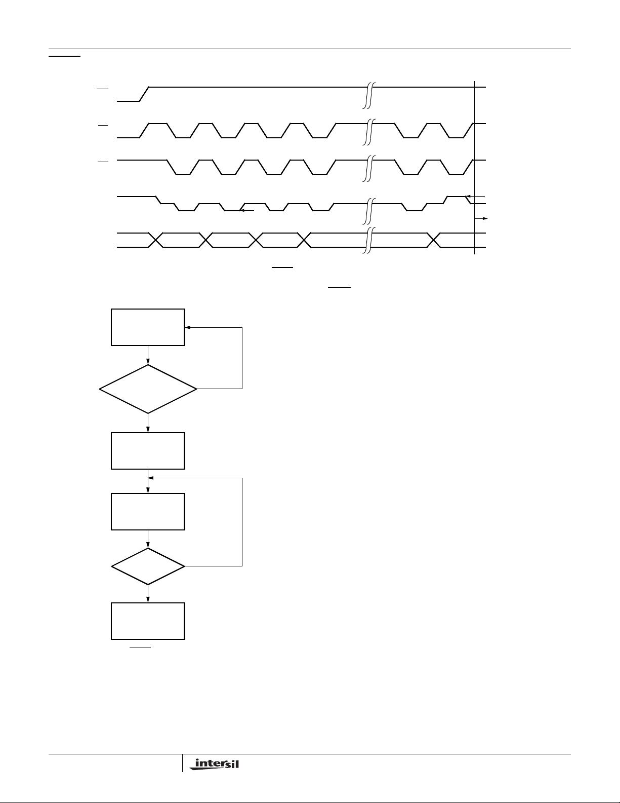
The Toggle Bit I/O
Last
WE
Write
CE
OE
I/O
6
Load Accum
From Addr N
FIGURE 3B. TOGGLE BIT SOFTWARE FLOW
6
Last Write
Compare
Accum with
Addr N
Compare
Ok?
Yes
X28C512
Ready
V
No
OH
V
OL
* Beginning and ending state of I/O6 will vary.
FIGURE 3A. TOGGLE BIT BUS SEQUENCE
*
The Toggle Bit can eliminate the chore of saving and
fetching the last address and data in order to implement
DATA
Polling. This can be especially helpful in an array
comprised of multiple X28C512, X28C513 memories that
are frequently updated. Toggle Bit Polling can also provide a
method for status checking in multiprocessor applications.
The timing diagram in Figure 3A illustrates the sequence of
events on the bus. The software flow diagram in Figure 3B
illustrates a method for polling the Toggle Bit.
HIGH Z
*
X28C512, X28C513
Ready
Hardware Data Protection
The X28C512, X28C513 provide three hardware features
that protect nonvolatile data from inadvertent writes.
- Noise Protection—A WE
pulse typically less than 10ns
will not initiate a write cycle.
- Default V
when V
Sense—All write functions are inhibited
CC
is 3.6V.
CC
- Write Inhibit—Holding either OE LOW, WE HIGH, or CE
HIGH will prevent an inadvertent write cycle during
power-up and power-down, maintaining data integrity.
Write cycle timing specifications must be observed
concurrently.
Software Data Protection
The X28C512, X28C513 offer a software controlled data
protection feature. The X28C512, X28C513 are shipped
from Intersil with the software data protection NOT
ENABLED; that is, the device will be in the standard
operating mode. In this mode data should be protected
during power-up/-down operations through the use of
external circuits. The host would then have open read and
write access of the device once V
The X28C512, X28C513 can be automatically protected
during power-up and power-down without the need for
external circuits by employing the software data protection
feature. The internal software data protection circuit is
enabled after the first write operation utilizing the software
algorithm. This circuit is nonvolatile and will remain set for
the life of the device unless the reset command is issued.
Once the software protection is enabled, the X28C512,
X28C513 are also protected from inadvertent and accidental
writes in the powered-up state. That is, the software
algorithm must be issued prior to writing additional data to
the device. Note: The data in the three-byte enable
sequence is not written to the memory array.
was stable.
CC
7
FN8106.2
June 7, 2006

Software Data Protection
www.BDTIC.com/Intersil
V
CC
0V
X28C512, X28C513
(VCC)
Data
Addr
CE
WE
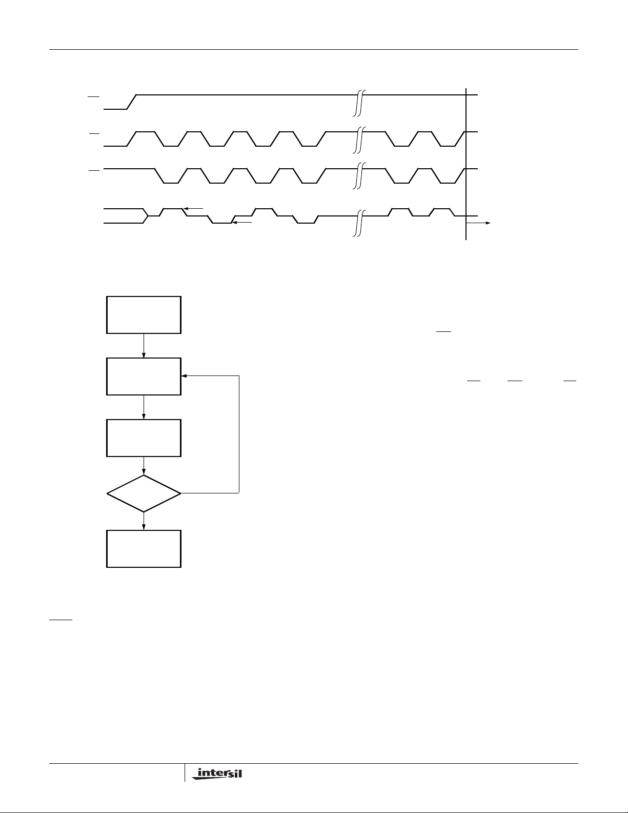
FIGURE 4A. TIMING SEQUENCE—SOFTWARE DATA PROTECT ENABLE SEQUENCE FOLLOWED BY BYTE OR PAGE WRITE
AAA
5555
Note: All other timings and control pins are per page write timing requirements
55
2AAA
A0
5555
≤ t
BLC MAX
Writes
ok
Byte
or
Page
t
WC
Write
Protected
Software Algorithm
Write Data AA
to Address
5555
Write Data 55
to Address
2AAA
Write Data 80
to Address
5555
Write Data XX
to any
Address
Optional
Byte/Page
Load Operation
Write Last
Byte to
Last Address
Selecting the software data protection mode requires the
host system to precede data write operations by a series of
three write operations to three specific addresses. Refer to
Figures 4A and 4B for the sequence. The three byte
sequence opens the page write window, enabling the host to
write from one to one hundred twenty-eight bytes of data.
Once the page load cycle has been completed, the device
will automatically be returned to the data protected state.
Regardless of whether the device has previously been
protected or not, once the software data protected algorithm
is used and data has been written, the X28C512, X28C513
will automatically disable further writes, unless another
command is issued to cancel it. If no further commands are
issued the X28C512, X28C513 will be write-protected during
power-down and after any subsequent power-up. The state
of A
while executing the algorithm is “don’t care”.
15
Note: Once initiated, the sequence of write operations
should not be interrupted.
After t
Re-Enters Data
Protected State
FIGURE 4B. WRITE SEQUENCE FOR SOFTWARE DATA
PROTECTION
WC
8
FN8106.2
June 7, 2006
Resetting Software Data Protection
www.BDTIC.com/Intersil
V
CC
X28C512, X28C513
Data
Addr
CE
WE
FIGURE 5B. SOFTWARE SEQUENCE TO DEACTIVA TE
SOFTWARE DATA PROTECTION
AAA
5555
Write Data AA
to Address
5555
Write Data 55
to Address
2AAA
Write Data A0
to Address
5555
Write Data AA
to Address
5555
Write Data 55
to Address
2AAA
Write Data 20
to Address
5555
55
2AAA
Note: All other timings and control pins are per page write timing requirements
FIGURE 5A. Reset Software Data Protection Timing Sequence
80
5555
In the event the user wants to deactivate the software data
protection feature for testing or reprogramming in an
EEPROM programmer, the following six step algorithm will
reset the internal protection circuit. After t
, the X28C512,
WC
X28C513 will be in standard operating mode.
AA
5555
55
2AAA
20
5555
≥ t
WC
Standard
Operating
Mode
System Considerations
Because the X28C512, X28C513 are frequently used in
large memory arrays, it is provided with a two-line control
architecture for both read and write operations. Proper
usage can provide the lowest possible power dissipation and
eliminate the possibility of contention where multiple I/O pins
share the same bus.
To gain the most benefit, it is recommended that CE
decoded from the address bus and be used as the primary
device selection input. Both OE
and WE would then be
common among all devices in the array. For a read operation
this assures that all deselected devices are in their standby
mode and that only the selected device(s) is/are outputting
data on the bus.
Because the X28C512, X28C513 have two power modes,
(standby and active), proper decoupling of the memory array
is of prime concern. Enabling CE
will cause transient current
spikes. The magnitude of these spikes is dependent on the
output capacitive loading of the I/Os. Therefore, the larger
the array sharing a common bus, the larger the transient
spikes. The voltage peaks associated with the current
transients can be suppressed by the proper selection and
placement of decoupling capacitors. As a minimum, it is
recommended that a 0.1µF high frequency ceramic
capacitor be used between V
and VSS at each device.
CC
Depending on the size of the array, the value of the capacitor
may have to be larger.
In addition, it is recommended that a 4.7µF electrolytic bulk
capacitor be placed between V
and VSS for each 8
CC
devices employed in the array. This bulk capacitor is
employed to overcome the voltage droop caused by the
inductive effects of the PC board traces.
be
Note: Once initiated, the sequence of write operations
should not be interrupted.
9
FN8106.2
June 7, 2006

X28C512, X28C513
www.BDTIC.com/Intersil
Active Supply Current vs Ambient Temperature
(mA)
I
CC
14
13
12
11
10
9
8
-55
-10 +125
Ambient Temperature (°C)
+35 +80
VCC = 5V
Standby Supply Current vs Ambient Temperature
0.24
0.22
0.2
0.18
(mA)
0.16
SB
I
0.14
VCC = 5V
ICC (RD) by Temperature Over Frequency
(mA)
I
CC
70
60
50
40
30
20
10
69
315
0
Frequency (MHz)
5.0 V
-55°C
+25°C
+125°C
12
CC
0.12
0.1
-55
-10 +125
Ambient Temperature (°C)
+35 +80
10
FN8106.2
June 7, 2006

X28C512, X28C513
www.BDTIC.com/Intersil
Absolute Maximum Ratings Recommended Operating Conditions
Temperature under bias
X28C512, X28C513 . . . . . . . . . . . . . . . . . . . . . . . .-10°C to +85°C
X28C512I/513I . . . . . . . . . . . . . . . . . . . . . . . . . . .-65°C to +135°C
X28C512M/513M . . . . . . . . . . . . . . . . . . . . . . . . .-65°C to +135°C
Storage temperature . . . . . . . . . . . . . . . . . . . . . . . .-65°C to +150°C
Voltage on any pin with respect to V
D.C. output current. . . . . . . . . . . . . . . . . . . . . . . . . . . . . . . . . . . 5mA
Lead temperature (soldering, 10s). . . . . . . . . . . . . . . . . . . . . .300°C
CAUTION: Stresses above those listed under “Absolute Maximum Ratings” may cause permanent damage to the device. This is a stress rating only; functional
operation of the device (at these or any other conditions above those listed in the operational sections of this specification) is not implied. Exposure to absolute
maximum rating conditions for extended periods may affect device reliability.
. . . . . . . . . . . . . . -1V to +7V
SS
DC Electrical Specifications Over recommended operating conditions, unless otherwise specified.
SYMBOL PARAMETER TEST CONDITIONS MIN MAX UNIT
VCC current (active) (TTL inputs) CE = OE = VIL, WE = VIH, All I/O’s = open, address
CC
VCC current (standby) (TTL inputs) CE = VIH, OE = VIL, All I/O’s = open, other inputs = V
VCC current (standby) (CMOS inputs) CE = VCC - 0.3V , OE = VIL, All I/O’s = Open, Other Inputs
Input leakage current VIN = VSS to V
I
LI
Output leakage current V
LO
Input LOW voltage -1 0.8 V
lL
Input HIGH voltage 2V
IH
Output LOW voltage IOL = 2.1mA 0.4 V
OL
Output HIGH voltage IOH = -400µA 2.4 V
OH
min. and VIH max. are for reference only and are not tested.
IL
inputs = 0.4V/2.4V Levels @ f = 5MHz
= V
IH
OUT
= VSS to VCC, CE = V
I
I
(Note 1)
(Note 1)
V
V
NOTE:
1. V
I
SB1
SB2
I
V
V
Temperature Range
Commercial . . . . . . . . . . . . . . . . . . . . . . . . . . . . . . . 0°C to +70°C
Industrial. . . . . . . . . . . . . . . . . . . . . . . . . . . . . . . . .-40°C to +85°C
Military . . . . . . . . . . . . . . . . . . . . . . . . . . . . . . . . .-55°C to +125°C
Supply Voltage Limits . . . . . . . . . . . . . . . . . . . . . . . . . . . . .5V ±10%
50 mA
IH
CC
IH
3mA
500 µA
10 µA
10 µA
+ 1 V
CC
Power-Up Timing
SYMBOL PARAMETER MAX UNIT
(Note 2) Power-up to read operation 100 µs
t
PUR
(Note 2) Power-up to write operation 5 ms
t
PUW
Capacitance T
SYMBOL PARAMETER TEST CONDITIONS MAX UNIT
(Note 2) Input/output capacitance V
C
I/O
(Note 2) Input capacitance VIN = 0V 10 pF
C
IN
= +25°C, f = 1MHz, VCC = 5V
A
= 0V 10 pF
I/O
Endurance and Data Retention
PARAMETER MIN MAX UNIT
Endurance 10,000 Cycles per byte
Endurance 100,000 Cycles per page
Data retention 100 Years
NOTE:
2. This parameter is periodically sampled and not 100% tested.
11
FN8106.2
June 7, 2006
X28C512, X28C513
www.BDTIC.com/Intersil
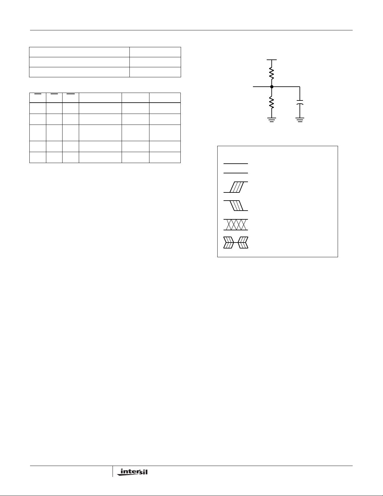
A.C. Conditions of Test
Input pulse levels 0V to 3V
Input rise and fall times 10ns
Input and output timing levels 1.5V
Mode Selection
CE OE WE MODE I/O POWER
LLH
LHL
HXX
XLX
XXH
Read D
Write D
Standby and write
inhibit
Write inhibit — —
Write inhibit — —
OUT
IN
High Z Standby
Active
Active
Equivalent A.C. Load Circuit
5V
1.92kΩ
Output
1.37KΩ
Symbol Table
WAVEFORM INPUTS OUTPUTS
Must be
steady
May change
from LOW
to HIGH
May change
from HIGH
to LOW
Don’t Care:
Changes
Allowed
N/A Center Line
100pF
Will be
steady
Will change
from LOW
to HIGH
Will change
from HIGH
to LOW
Changing:
State Not
Known
is High
Impedance
12
FN8106.2
June 7, 2006
X28C512, X28C513
www.BDTIC.com/Intersil
AC Electrical Specifications Over the recommended operating conditions, unless otherwise specified.
X28C512-90 X28C512-12 X28C512-15 X28C512-20 X28C512-25
X28C513-90 X28C513-12 X28C513-15 X28C513-20 X28C513-25
SYMBOL PARAMETER
READ CYCLE LIMITS
t
RC
t
t
t
OE
t
(Note 3)
t
OLZ
(Note 3)
t
Read cycle time 90 120 150 200 250 ns
Chip enable access time 90 120 150 200 250 ns
CE
Address access time 90 120 150 200 250 ns
AA
Output enable access time 40 50 50 50 50 ns
CE
LZ
HZ
LOW to active output 0 0 0 0 0 ns
LOW to active output 0 0 0 0 0 ns
OE
CE
HIGH to high Z output 40 50 50 50 50 ns
(Note 3)
OE
t
OHZ
(Note 3)
t
OH
HIGH to high Z output 40 50 50 50 50 ns
Output hold from address change 0 0 0 0 0 n s
MIN MAX MIN MAX MIN MAX MIN MAX MIN MAX
UNIT
Read Cycle
Address
CE
OE
WE
Data I/O
NOTE:
3. t
min., tHZ, t
LZ
point when CE
t
RC
t
CE
t
OE
V
IH
t
OLZ
t
LZ
HIGH Z
min., and t
OLZ
or OE return HIGH (whichever occurs first) to the time when the outputs are no longer driven.
are periodically sampled and not 100% tested. tHZ max. and t
OHZ
Data Valid
t
OH
t
AA
max. are measured, with CL = 5pF from the
OHZ
Data Valid
t
OHZ
t
HZ
13
FN8106.2
June 7, 2006

X28C512, X28C513
www.BDTIC.com/Intersil
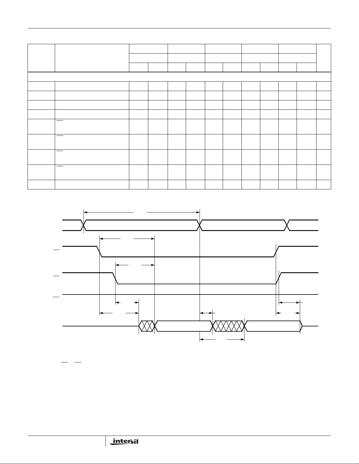
Write Cycle Limits
SYMBOL PARAMETER MIN MAX UNIT
(Note 4) Write cycle time 10 ms
t
WC
t
AS
t
AH
t
CS
t
CH
t
CW
t
OES
t
OEH
t
WP
t
WPH
t
DV
t
DS
t
DH
t
DW
t
BLC
Address setup time 0 ns
Address hold time 50 ns
Write setup time 0 ns
Write hold time 0 ns
CE pulse width 100 ns
OE HIGH setup time 10 ns
OE HIGH hold time 10 ns
WE pulse width 100 ns
WE High recovery 100 ns
Data valid 1µs
Data setup 50 ns
Data hold 0 ns
Delay to next write 10 µs
Byte load cycle 0.2 100 µs
WE Controlled Write Cycl e
t
WC
Address
t
AS
t
CS
CE
OE
t
OES
WE
t
DV
Data In
Data Out
NOTE:
is the minimum cycle time to be allowed from the system perspective unless polling techniques are used. It is the maximum time the device
4. t
WC
requires to complete the internal write operation.
t
AH
t
CH
t
t
DS
OEH
Data Valid
HIGH Z
t
DH
t
WP
14
FN8106.2
June 7, 2006

CE Controlled Write Cycle
www.BDTIC.com/Intersil
Address
CE
t
OE
WE
Data In
Data Out
OES
X28C512, X28C513
t
WC
t
AS
t
CS
t
DV
t
AH
t
CW
t
WPH
t
OEH
t
CH
Data Valid
t
DS
HIGH Z
t
DH
Page Write Cycle
OE
(Note 5)
CE
t
WP
WE
Address*
(Note 6)
I/O
*For each successive write within the page write operation, A7-A
writes to an unknown address could occur.
t
WPH
Byte 0 Byte 1 Byte 2 Byte n Byte n+1 Byte n+2
NOTES:
5. Between successive byte writes within a page write operation, OE
data from another memory device within the system for the next write; or with WE
6. The timings shown above are unique to page write operations. Individual byte load operations within the page write must conform to either the
or WE controlled write cycle timing.
CE
t
BLC
Last Byte
t
WC
should be the same or
15
can be strobed LOW: e.g. this can be done with CE and WE HIGH to fetch
HIGH and CE LOW effectively performing a polling operation.
15
FN8106.2
June 7, 2006

DATA Polling Timing Diagram (Note 7)
www.BDTIC.com/Intersil
X28C512, X28C513
Address A
CE
WE
OE
I/O
7
n
Toggle Bit Timing Diagram
CE
WE
t
OEH
A
n
t
OEH
D
= X
IN
D
= X D
OUT
t
WC
A
n
t
OES
t
DW
= X
OUT
t
OES
OE
I/O
6
HIGH Z
*
t
WC
*Starting and ending state will vary, depending upon actual t
NOTE:
7. Polling operations are by definition read cycles and are therefore subject to read cycle timings.
WC
t
DW
*
.
16
FN8106.2
June 7, 2006
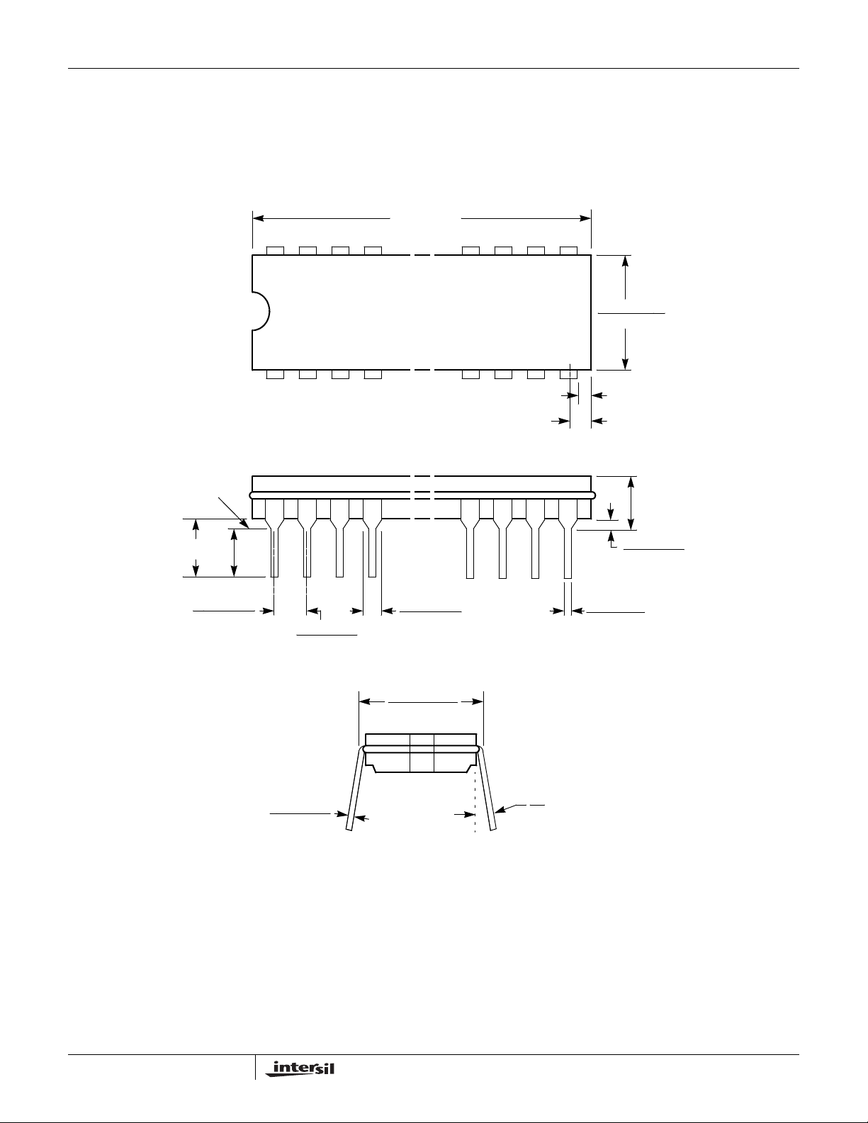
Packaging Information
www.BDTIC.com/Intersil
Pin 1
X28C512, X28C513
32-Lead Hermetic Dual In-Line Package Type D
1.690 (42.95)
Max.
0.610 (15.49)
0.500 (12.70)
0.005 (0.13) Min.
0.100 (2.54) Max.
Seating
Plane
0.150 (3.81) Min.
0.200 (5.08)
0.125 (3.18)
0.110 (2.79)
0.090 (2.29)
Typ. 0.100 (2.54)
0.015 (0.38)
0.008 (0.20)
0.065 (1.65)
0.033 (0.84)
Typ. 0.055 (1.40)
0.620 (15.75)
0.590 (14.99)
Typ. 0.614 (15.60)
0.232 (5.90) Max.
0.060 (1.52)
0.015 (0.38)
0.023 (0.58)
0.014 (0.36)
Typ. 0.018 (0.46)
0°
15°
NOTE: ALL DIMENSIONS IN INCHES (IN PARENTHESES IN MILLIMETERS)
17
FN8106.2
June 7, 2006
Packaging Information
www.BDTIC.com/Intersil
0.015 (0.38)
0.003 (0.08)
X28C512, X28C513
32-Pad Ceramic Leadless Chip Carrier Package Type E
0.300 (7.62)
BSC
0.150 (3.81) BSC
0.020 (0.51) x 45° Ref.
0.095 (2.41)
Pin 1
0.075 (1.91)
0.022 (0.56)
0.006 (0.15)
DIA.
0.200 (5.08)
BSC
0.028 (0.71)
0.022 (0.56)
(32) Plcs.
0.015 (0.38)
Min.
0.050 (1.27) BSC
0.458 (11.63)
0.442 (11.22)
0.458 (11.63)
--
0.055 (1.39)
0.045 (1.14)
TYP. (4) PLCS.
0.040 (1.02) x 45° Ref.
Typ. (3) Plcs.
0.560 (14.22)
0.540 (13.71)
0.120 (3.05)
0.060 (1.52)
0.558 (14.17)
--
0.088 (2.24)
0.050 (1.27)
0.400 (10.16)
BSC
Pin 1 Index Corner
NOTE:
1. ALL DIMENSIONS IN INCHES (IN PARENTHESES IN MILLIMETERS)
2. TOLERANCE: ±1% NLT ±0.005 (0.127)
18
FN8106.2
June 7, 2006

Packaging Information
www.BDTIC.com/Intersil
0.830 (21.08) Max.
X28C512, X28C513
32-Lead Ceramic Flat Pack Type F
1.228 (31.19)
1.000 (25.40)
Pin 1 Index
132
0.019 (0.48)
0.015 (0.38)
0.050 (1.27) BSC
0.045 (1.14) Max.
0.007 (0.18)
0.004 (0.10)
0.370 (9.40)
0.270 (6.86)
0.030 (0.76)
Min.
NOTE: ALL DIMENSIONS IN INCHES (IN PARENTHESES IN MILLIMETERS)
0.440 (11.18)
0.430 (10.93)
0.347 (8.82)
0.330 (8.38)
0.005 (0.13) Min.
0.120 (3.05)
0.090 (2.29)
0.026 (0.66)
Min.
19
FN8106.2
June 7, 2006

X28C512, X28C513
www.BDTIC.com/Intersil
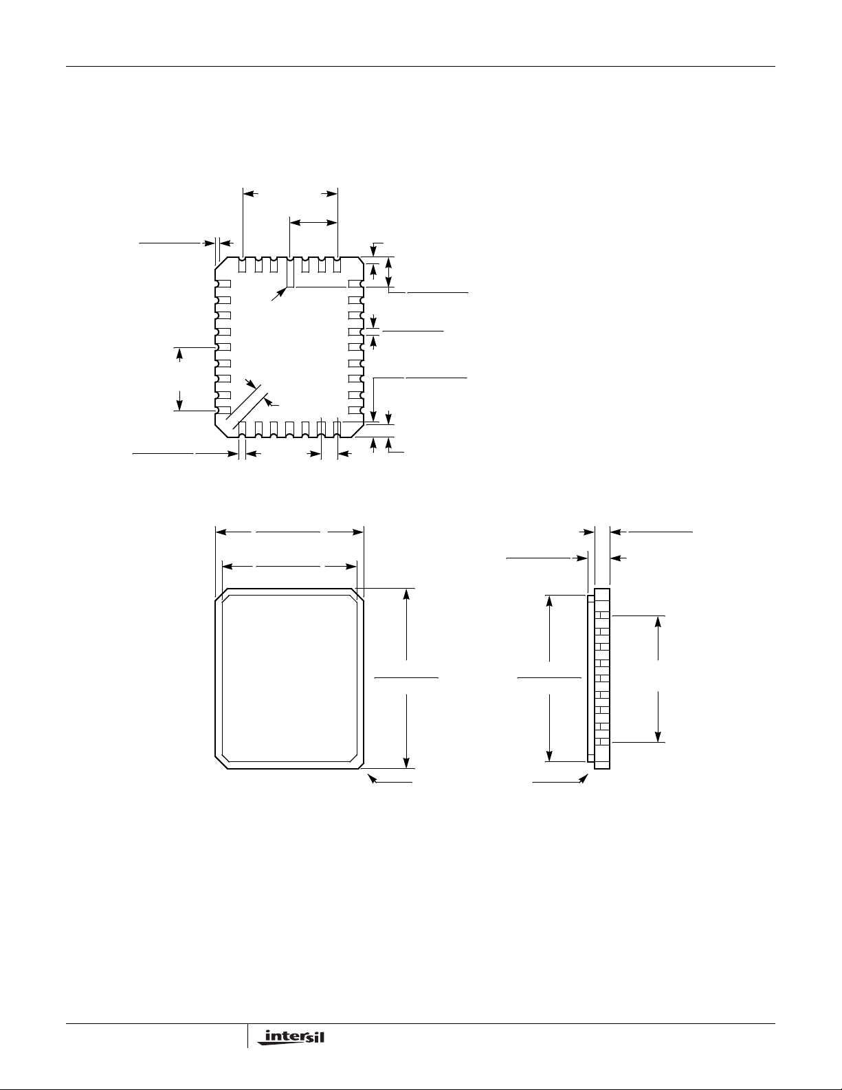
Plastic Leaded Chip Carrier Packages (PLCC)
0.042 (1.07)
0.048 (1.22)
NE
0.020 (0.51) MAX
3 PLCS
PIN (1)
IDENTIFIER
C
L
D1
D
0.050 (1.27)
MIN
0.025 (0.64)
MIN
0.042 (1.07)
0.056 (1.42)
0.050 (1.27) TP
ND
E1
VIEW “A” TYP.
C
L
E
0.026 (0.66)
0.032 (0.81)
0.013 (0.33)
0.021 (0.53)
(0.12)
0.005
0.004 (0.10) C
0.025 (0.64)
0.045 (1.14)
D2/E2
D2/E2
A1
A
-C-
M
- B SAS
R
VIEW “A”
0.015 (0.38)
MIN
SEATING
PLANE
DS
32 LEAD PLASTIC LEADED CHIP CARRIER PACKAGE
INCHES MILLIMETERS
SYMBOL
NOTESMIN MAX MIN MAX
A 0.125 0.140 3.18 3.55 -
A1 0.060 0.095 1.53 2.41 -
D 0.485 0.495 12.32 12.57 -
D1 0.447 0.453 11.36 11.50 3
D2 0.188 0.223 4.78 5.66 4, 5
E 0.585 0.595 14.86 15.11 -
E1 0.547 0.553 13.90 14.04 3
E2 0.238 0.273 6.05 6.93 4, 5
N28 286
ND 7 7 7
NE 9 9 7
Rev. 0 7/98
NOTES:
1. Controlling dimension: INCH. Converted millimeter dimensions are not necessarily exact.
2. Dimensions and tolerancing per ANSI Y14.5M-1982.
3. Dimensions D1 and E1 do not include mold protrusions. Allowable mold protrusion is 0.010 inch (0.25mm) per side.
Dimensions D1 and E1 include mold mismatch and are measured at the extreme material condition at the body parting
line.
4. To be measured at seating plane contact point.
-C-
5. Centerline to be determined where center leads exit plastic
body.
6. “N” is the number of terminal positions.
7. ND denotes the number of leads on the two shorts sides of the
package, one of which contains pin #1. NE denotes the number of leads on the two long sides of the package.
N32.45x55 (JEDEC MS-016AE ISSUE A)
20
FN8106.2
June 7, 2006

X28C512, X28C513
www.BDTIC.com/Intersil
Ceramic Pin Grid Array Package (CPGA)
15 17 19 21 22
13
14 16 18 20 23
12 11 25 26
10 9 27
8 7 29 30
6 31
5 2 36 34 32
Typ. 0.180 (.010)
(4.57 ± .25)
4 Corners
4 3 1 35 33
Typ. 0.180 (.010)
(4.57 ± .25)
4 Corners
Pin 1 Index
G36.760x760A
36 LEAD CERAMIC PIN GRID ARRAY PACKAGE
24
28
A
A
NOTE: Leads 5, 14, 23, & 32
Typ. 0.100 (2.54)
All Leads
0.008 (0.20)
0.050 (1.27)
0.120 (3.05)
0.100 (2.54)
0.072 (1.83)
0.062 (1.57)
0.770 (19.56)
0.750 (19.05)
SQ
A
A
NOTE: All dimensions in inches (in parentheses in millimeters).
0.020 (0.51)
0.016 (0.41)
0.185 (4.70)
0.175 (4.45)
Rev. 0 12/05
All Intersil U.S. products are manufactured, assembled and tested utilizing ISO9000 quality systems.
Intersil Corporation’s quality certifications can be viewed at www.intersil.com/design/quality
Intersil products are sold by description only. Intersil Corporation reserves the right to make changes in circuit design, software and/or specifications at any time without
notice. Accordingly, the reader is cautioned to verify that data sheets are current before placing orders. Information furnished by Intersil is believed to be accurate and
reliable. However, no responsibility is assumed by Intersil or its subsidiaries for its use; nor for any infringements of patents or other rights of third parties which may result
from its use. No license is granted by implic atio n or other wise u nde r any p a tent or patent rights of Intersil or its subsidiaries.
For information regarding Intersil Corporation and its products, see www.intersil.com
21
FN8106.2
June 7, 2006
 Loading...