Intersil SP600 Datasheet

Semiconductor
E
PART WITHDRAWN
Features
• Maximum Rating. . . . . . . . . . . . . . . . . . . . . . . . . . . 500V
• Ability to Interface and Drive Standard and Current
Sensing N-Channel Power MOSFET/IGBT Devices
• Creation and Management of a Floating Power Supply
for Upper Rail Drive
• Simultaneous Conduction Lockout
PROCESS OBSOLETE
NO NEW DESIGNS
SP600
July 1998 File Number 2428.4
Half Bridge 500VDC Driver
The SP600 is a smart power high voltage integrated circuit
(HVIC) optimized to drive MOS gated power devices in halfbridge topologies. It provides the necessary control and
management for PWM motor drive, power supply, and UPS
applications.
• Overcurrent Protection
• Single Low Current Bias Supply Operation
• Latch Immune CMOS Logic
• Peak Drive in Excess of 0.5A
Pinout
1
FAULT
I
2
TRIPSEL
V
3
BIAS
V
4
DD
V
5
SS
TRIP
6
L
7
CL1
G2L
8
G1L
9
D1L
10
V
11
DF
SP600 (PDIP)
TOP VIEW
22
TOP
21
BOT
20
NC
D1U
19
G1U
18
G2U
17
CL2
16
TRIP
15
PHAS
14
V
13
OUT
V
12
BS
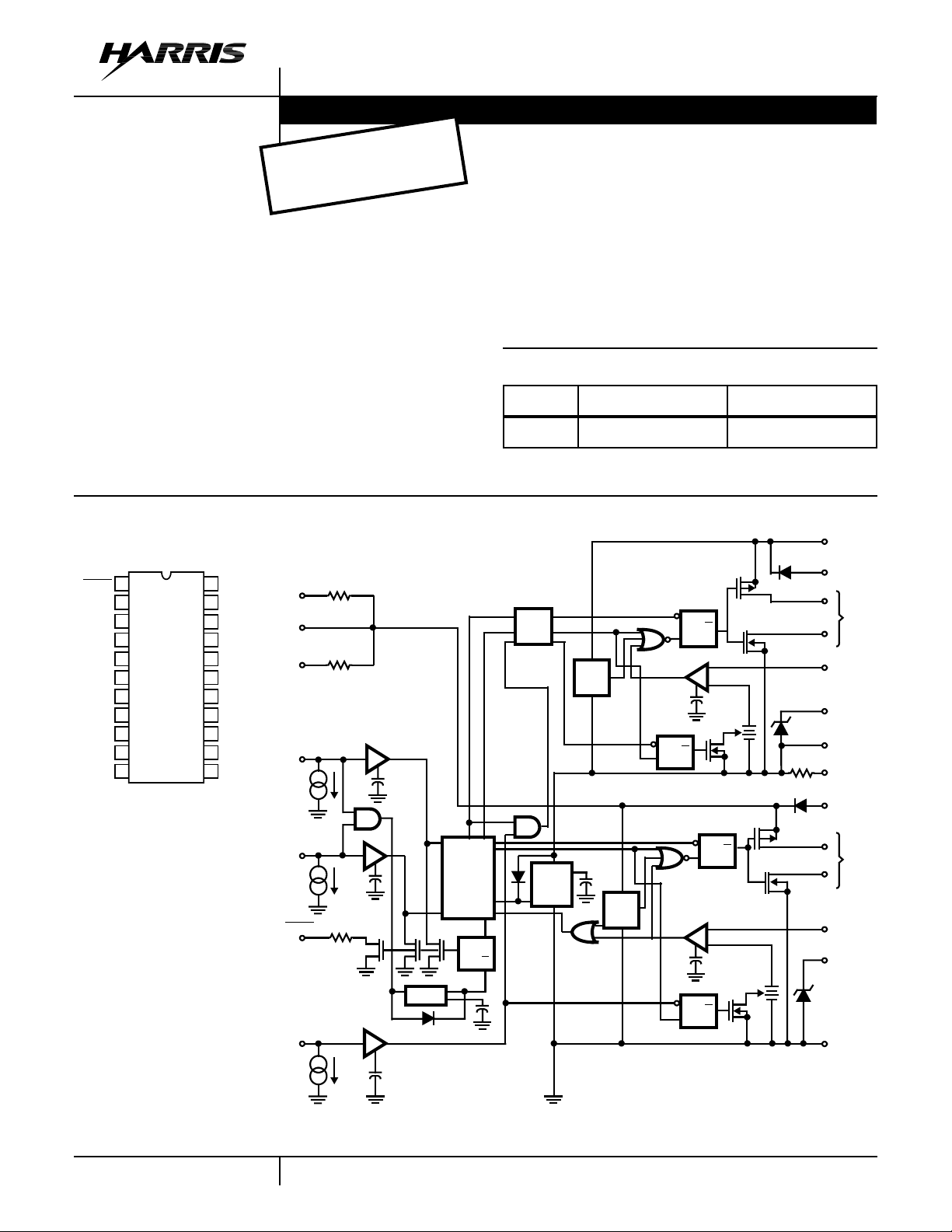
Functional Block Diagram
10Ω R
V
BIAS
3
V
DD
4
V
DF
11
U
TOP
22
BOT
21
FAULT
1
I
TRIPSEL
2
3.5Ω R
750Ω R
ND
BS
Ordering Information
PART TEMPERATURE PACKAGE
SP600 -40oC to +85oC 22 Lead Plastic DIP
V
BS
12
D1U
19
3.5Ω R
G1U
18
G2U
17
TRIP
15
CL2
16
PHASE
14
O
13
D1L
10
G1L
9
G2L
8
TRIP
6
CL1
7
V
SS
5
U
V
OUT
LOWER UPPER
L
I
ONT
I
LEVEL
OFFT
SHIFT
UV
LOCK
OUT
I
TRIPSEL
I
ONB
I
I
TRIPSEL
OFFB
UV
LOCK
OUT
CMOS
TIMING
AND
CONTROL
F
S
Q
R
FILTER
FAULT
V
OUT
SENSE
AND
FILTER
S
Q
R
+
-
S
Q
R
S
Q
R
+
-
S
Q
R
1
CAUTION: These devices are sensitive to electrostatic discharge; follow proper IC Handling Procedures.
Copyright © Harris Corporation 1998

SP600
Absolute Maximum Ratings Full Temperature Range, All
Thermal Information
VoltageReferenced to VSSUnless Otherwise Noted. Note 1, Note 2.
Low Voltage Power Supply, V
Floating Low Voltage Boot Strap . . . . . . . . . . . . . . . . . . . . . . 18V
Power Supply to Phase, V
Low Voltage Signal Pins
Fault, I
TRIPSEL
, VDD, TRIPL, CL1, G2L . . .-0.5VDC to VDD +0.5
G1L, D1L, VDF, TOP, BOT
CL2, TRIPU, G1U, G2U, D1U to Phase. . . . -0.5
(Note 1) . . . . . . . . . . . . . . 18V
BIAS
BS
VDC
DC
DC
to VBS +0.5
Thermal Resistance θ
JA
Plastic DIP Package . . . . . . . . . . . . . . . . . . . . . . . . 75oC/W
Maximum Package Power Dissipation at TA = +85oC, P
O
Plastic DIP Package . . . . . . . . . . . . . . . . . . . . . . . . . . . . . 500mW
Operating Ambient Temperature Range, TA . . . . . . .-25oC to +85oC
Storage Temperature Range, TS. . . . . . . . . . . . . . .-40oC to +150oC
Lead Temperature (Soldering 10s) . . . . . . . . . . . . . . . . . . . .+265oC
High Voltage Pins
Phase, V
(VBS,V
. . . . . . . . . . . . . . . . . . . . . . . . . . . . . . . . 500V
PHASE
, TRIPU, CL2, G2U and D1U: 0V-18V Higher Than
OUT
DC
Phase)
Dynamic High Voltage Rating Phase,. . . . . . . . . . . . . 10,000V/µs
DV
PHASE/DT
NOTES:
1. Care must betaken inthe application of V
Prolonged high peakcurrents mayresult if+15V
If it is desirable to switch the 15V
2. Consult factory for additional package offerings.
CAUTION: Stresses above those listed in “Absolute Maximum Ratings” may cause permanent damage to the device. This is a stress only rating and operation
of the device at these or any other conditions above those indicated in the operational sections of this specification is not implied.
source or if a CDD is larger, additional series impedance may be required.
DC
Electrical Specifications (V
asnot toimpose high peak dissipation demands on arelatively smallmetallized noise dropping resistor (RND).
BIAS
BIAS
is applied abruptlyand/or ifthe localbypass capacitorCDDis large. Itis suggestedthat CDDbe ≤ 10MFD.
DC
= 15V, Pulsed <300ms), Unless Otherwise Noted, All Parameters Referenced to
VSSExcept TRIPU, CL2, G1U, D1U, and VBSReferenced to PHASE. DF:VDFto VBS,
CF: VBS to PHASE
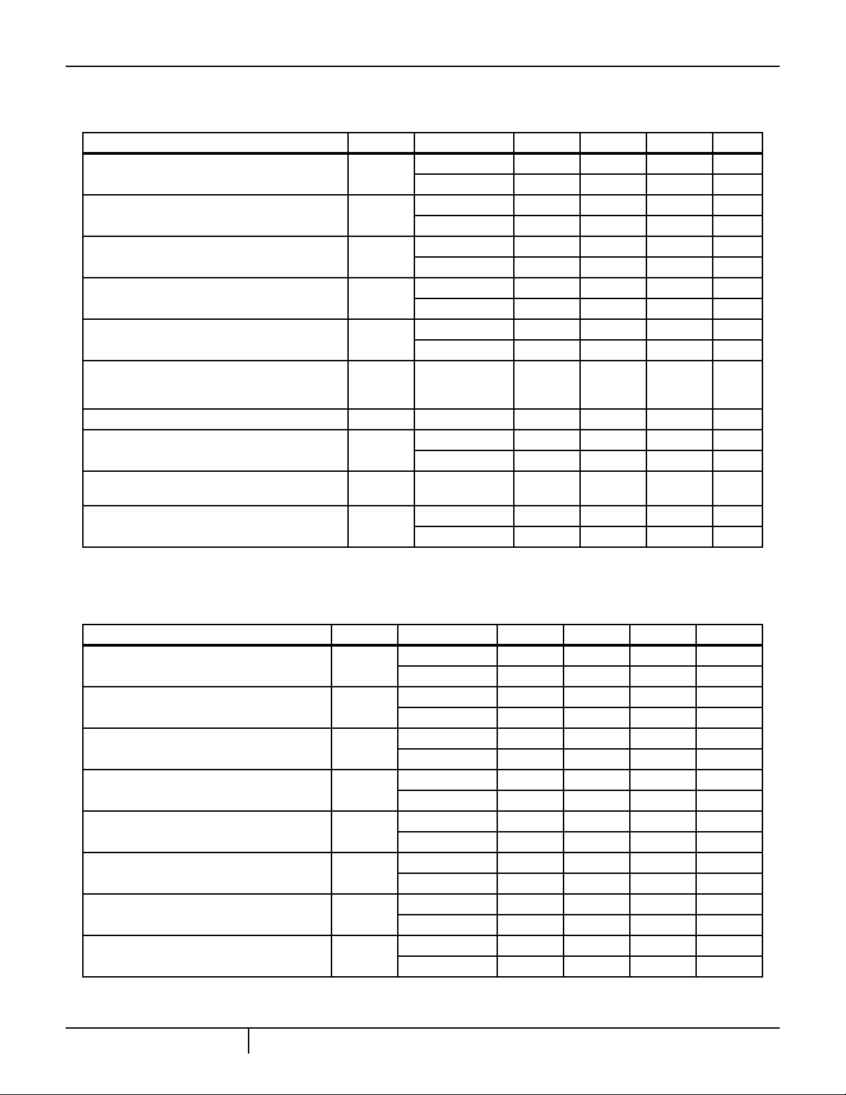
PARAMETER SYMBOL TEMP MIN TYP MAX UNITS
DC CHARACTERISTICS
Input Current (5V < V
TOP
, V
BOT
, V
TRIPSEL
< 15V) I
IN
+25oC - 20 30 µA
-40oC to +85oC - 30 33 µA
I
Quiescent Current (All Inputs Low) I
BIAS
BIAS
L
+25oC - 1.7 2.05 mA
-40oC to +85oC - 1.7 2.1 mA
I
Quiescent Current
BIAS
(V
≥ V
OUT
, and All Inputs Low)
BIAS
IBS Quiescent Current Bootstrap Supply I
I
BIAS
BS
H
+25oC - 1.7 2.05 mA
-40oC to +85oC - 1.7 2.1 mA
+25oC - 875 1000 µA
-40oC to +85oC - 900 1060 µA
TOP Threshold Level V
TOP
+25oC 789V
-40oC to +85oC 6.95 8 9.1 V
BOTTOM Threshold Level V
BOT
+25oC 789V
-40oC to +85oC 6.9 8 9.1 V
Current TRIPSELECT Threshold Level V
TRIPSEL
+25oC 789V
-40oC to +85oC 6.95 8 9.1 V
Trip Lower and Upper Comparator Threshold
Level - Normal (I
TRIPSEL
= VSS)
Trip Lower and Upper Comparator Threshold
Level - Boost (I
V
TRIP L/U
N
TRIPSEL
= VDD) % of Measured
Under Voltage Lockout Thresholds (VDD and VBS)V
V
TRIP L/U
V
TRIP L/U
LOCK
N
+25oC 90 105 125 mV
-40oC to +85oC 90 105 127 mV
B
+25oC 110 130 150 %
-40oC to +85oC 109 130 152 %
+25oC 9 10 11.5 V
-40oC to +85oC 9.7 10.5 11.8 V
Phase Out of Status Voltage Threshold (PHASE) V
OSVT
+25oC 579V
-40oC to +85oC 4.7 7 9.6 V
2

SP600
Electrical Specifications (V
= 15V, Pulsed <300ms), Unless Otherwise Noted, All Parameters Referenced to
BIAS
VSSExcept TRIPU, CL2, G1U, D1U, and VBSReferenced to PHASE. DF:VDFto VBS,
CF: VBS to PHASE (Continued)
PARAMETER SYMBOL TEMP MIN TYP MAX UNITS
Faultbar Impedance at I
Upper/LowerSourceImpedances(I
Upper/Lower Sink Impedances (I
= 1mA RF +25oC 500 760 1000 Ω
FBAR
SOURCE
SINK
=10mA) R
= 10mA) R
Bootstrap Supply Current Limiting Impedance R
Noise Dropping Resistor Impedance R
High Voltage Leakage (500V VBS, V
OUT
, PHASE,
TRIPU, CL2, G1U, G2U, and D1U to VSS. All other
Pins at VSS)
Miller Clamp Diodes; D1U and D1L (ID = 10mA) V
Noise Clamping Zeners; CL2 and CL1 (IZ = 10mA) V
CL2/1-LOW
Noise Clamping Zeners; CL2 and CL1 (IZ = 50mA) V
V
Limiting Resistance R
OUT
NOTE: Maximum Steady State ÷ 15VDC Supply Current = I
SO L/U
SI L/U
BS
ND
I
LK
D1U/L
CL2/1-
HIGH
O
BIAS
-40oC to +85oC 450 760 1100 Ω
+25oC 121723Ω
-40oC to +85oC 7 17 29 Ω
+25oC 8 12 16 Ω
-40oC to +85oC 5 12 20 Ω
+25oC 2 3.5 5 Ω
-40oC to +85oC 1.4 3.5 5.6 Ω
+25oC 6 10 14 Ω
-40oC to +85oC 5.4 10 14.6 Ω
+25oC-13µA
+25oC 0.40 0.90 1.40 V
+25oC 6.35 6.61 6.85 V
-40oC to +85oC 6.15 6.61 7.15 V
+25oC 7.0 8.5 8.0 V
+25oC 2 3.5 5 Ω
-40oC to +85oC 1.4 3.5 5.6 Ω
÷I
BS
L
Switching Specifications (All Referenced to V
DF: VDF to VBS, CF: VBS to PHASE)
PARAMETER SYMBOL TEMP MIN TYP MAX UNITS
Refresh One Shot Timer t
Delay Time of Trip I/U Voltage (I
TRIPSEL
G2U/G2L Low (50% Overdrive)
Delay Time of Trip I Voltage (I
TRIPSEL
Faultbar Low
Delay Time of Phase Out of Status to Faultbar
Low (TOP High)
Minimum Logic Input Pulse Width: TOP and
BOTTOM
Minimum G1U/G1L On Time t
Minimum Pulsed Off Time, G2U/G2L t
Turn On Delay Time of G1U (BISTATE MODE) t
low) to
low) to
, Except: TRIPU, Cl2, G1U, G2U, and D1U Referenced to PHASE.
SS
REF
+25oC 200 350 500 µs
-40oC to +85oC 180 350 540 µs
t
OFF
TN
+25oC 234µs
-40oC to +85oC 1.85 3 4.35 µs
t
FN
+25oC 234µs
-40oC to +85oC 1.85 3 4.35 µs
t
OSVF
+25oC 500 700 900 ns
-40oC to +85oC 400 700 1050 ns
t
MINIW
+25oC 300 430 600 ns
-40oC to +85oC 275 430 660 ns
ON
+25oC 1.6 2.3 3.1 µs
-40oC to +85oC 1.5 2.4 3.4 µs
OFF
+25oC 1.3 2.0 3.4 µs
-40oC to +85oC 1.05 2.1 3.9 µs
ON
D
+25oC 2.5 3.2 4.5 µs
-40oC to +85oC 2.1 3.3 5.2 µs
3
 Loading...