

Page 1

User’s Manual
ISL71010BM50EV1Z
High Reliability
User’s Manual: Evaluation Board
Rev 0.00 Oct 2017
Page 2

USER’S MANUAL
ISL71010BM50EV1Z
Evaluation Board
Oct 24, 2017
1. Overview
The ISL71010BM50EV1Z evaluation board measures the performance of the high precision 5.0V ISL71010B50
voltage reference. The reference has a wide input voltage range from 7V to 30V and an initial accuracy of ±0.05%. The
voltage noise of 4.2µV
makes the ISL71010B50 ideal for high-end applications.
The evaluation board includes voltage input test points (VIN and GND) for a power supply input, as well as a pair of
test points for the output (VOUT and GND). The resistor location designated as R
designated as C
style resistors and C
connected to VOUT by installing a jumper at J1.
allow for VOUT output load testing. The R2 resistor location accepts surface mount or through-hole
3
1.1 Key Features
• Voltage input test points for connection of a power supply
• Convenient output test points to measure VOUT of the voltage reference
•R
and C3 allow for VOUT output load testing
2
• Additional R-C damper network can be connected at VOUT by installing a jumper at J1
in the 0.1Hz to 10Hz range and maximum output voltage temperature coefficient of 10ppm/°C
P-P
and the capacitor location
2
comes populated with a 0.1µF load capacitor. Additionally, an R-C damper network can be
3
UG136
Rev.0.00
1.2 Specifications
This evaluation board has been configured and optimized for the following conditions:
•V
= 7V to 30V
IN
• 10µF and 0.1µF input decoupling capacitors, 1nF compensation capacitor, and 0.1µF load capacitor
•R
load resistance of ≥250Ω
2
• Selectable 10µF and 2.21kΩ damper network at the output by installing a jumper at J1
• Board temperature: +25°C
1.3 Ordering Information
Part Number Output Voltage (V) Description
ISL71010BM50EV1Z 5.0V Evaluation board
1.4 Related Literature
• For a full list of related documents, visit our website
• ISL71010B50
• ISL71010B25
product page
product page
UG136 Rev.0.00 Page 2 of 12
Oct 24, 2017
Page 3
ISL71010BM50EV1Z 1. Overview
10µF 0.1µF
Chip Select
Serial Clock
Serial Data I/O
VDD VREF
SCLK
SDIO
CSb
OUTxS
GND
DACOUTx
VIN
VREF
0.1µF
OUTxF
DAC
1
2
3
4
DNC
GND
VOUT
TRIM
6
8
7
5
DNC
DNC
COMP
VIN
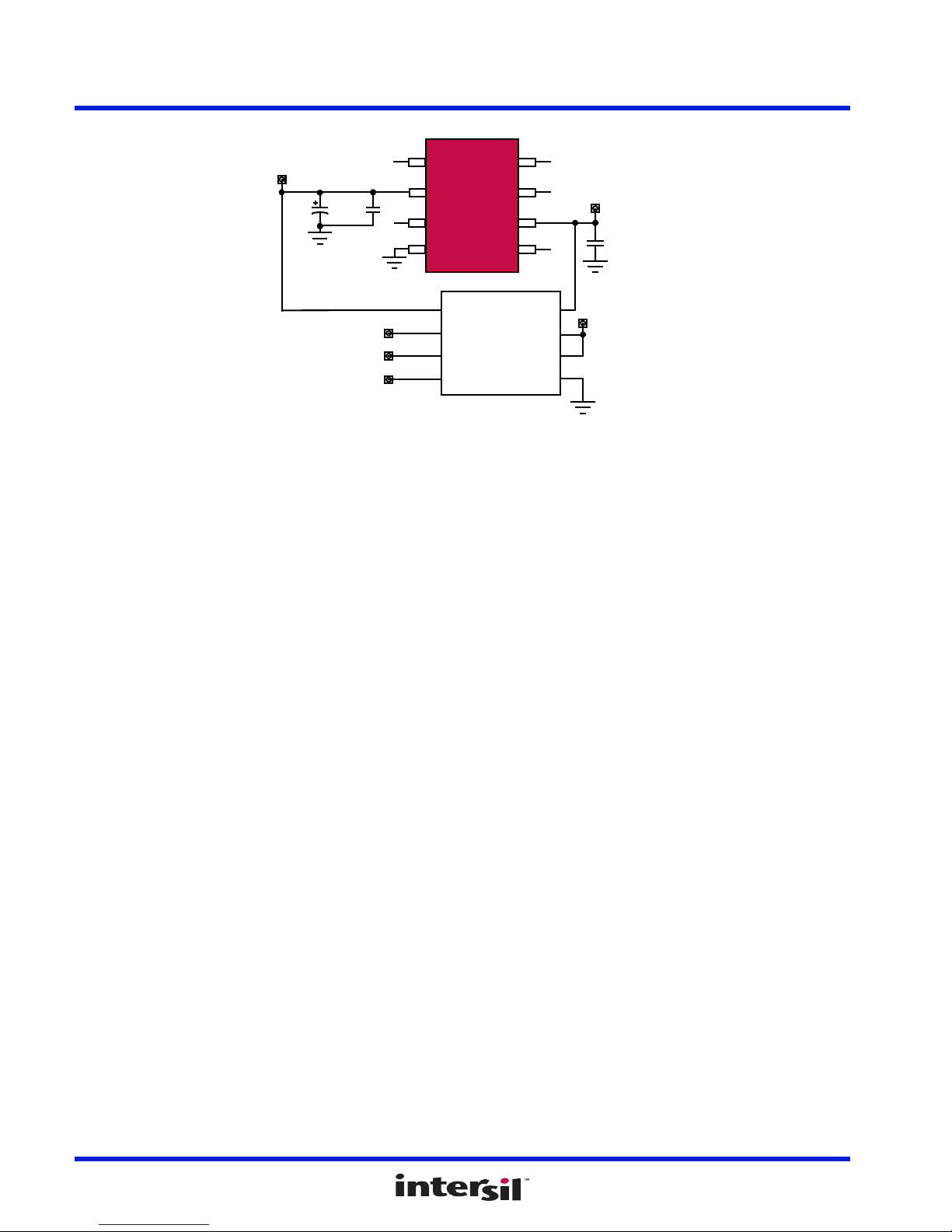
Figure 1. ISL71010BM50EV1Z Block Diagram
UG136 Rev.0.00 Page 3 of 12
Oct 24, 2017
Page 4
ISL71010BM50EV1Z 2. Functional Description
2. Functional Description
The ISL71010BM50EV1Z evaluation board provides a simple platform to demonstrate the features and evaluate the
performance of the ISL71010B50 voltage reference. It provides easy access to the pins of the ISL71010B50 IC. The
schematic, bill of materials, and top silkscreen for the board are shown on pages 6
Figures 8
through 18 show performance data taken using the ISL71010BM50EV1Z evaluation board and basic lab
equipment.
The following sections explain how to use the evaluation board.
2.1 Basic Layout of the Evaluation Board
Refer to Figure 3 on page 6 or the actual ISL71010BM50EV1Z evaluation board for the basic layout.
The schematic of the evaluation board is shown in Figure 4 on page 6
ISL71010B50 voltage reference (U1), input decoupling capacitors (C
load capacitor (C
loads. The R
). Different resistor values can be applied at (R2) for testing of the voltage reference at different
3
resistor location accepts surface mount or through-hole style resistors.
2
The power supply leads attach to TP1 and TP2 (VIN, GND). The ISL71010B50 IC requires a DC supply in the
range of 7.0V to 30V for proper operation. The power supply should be capable of delivering 100mA of current.
The output is measured at test points TP3 and TP4 (VOUT, GND), and is best measured with a high precision voltmeter
(such as the Agilent 3458A 8 - 1/2 digit multimeter).
The R-C damper network (R
, C4) is populated and can be connected to the reference output by adding a shunt to
1
the R-C jumper (J1). The damper network improves stability by reducing transient load ringing with high value
(>0.47µF) load capacitance.
. The ISL71010BM50EV1Z contains the
1
through 8.
, C2), a compensation capacitor (C5), and a
2.1.1 Components Parts List
Table 1. Components Parts List
Reference Designator Value Description
C
1
C
2
C
3
C
4
C
5
R
1
R
2
U1 ISL71010BMB50Z SOIC 8 Ld package
J1 DNP Damper jumper
10µF Bypass capacitor
0.01µF Bypass capacitor
0.1µF Load capacitor
10µF Damper capacitor
1nF Compensation capacitor
2.21kΩ Damper resistor
DNP Optional load resistor
2.2 Operating Range
The ISL71010B50 IC requires a VIN DC supply in the range of 7.0V to 30V for proper operation. The power
supply should be capable of delivering 100mA of current.
The ISL71010B50 IC V
load resistor should be selected to be ≥250Ω. Note: With V
≤75mA.
can source 20mA of current and sink -10mA of current. For normal operation the R2
OUT
shorted to ground the IC will limit the current to
OUT
UG136 Rev.0.00 Page 4 of 12
Oct 24, 2017
Page 5

ISL71010BM50EV1Z 2. Functional Description
7V to 30V
DC Power Supply
ISL71010BM50EV1ZEVAL1Z
-
+
C4
C3
TP1
R1
R2
VIN
VOUT
LOAD
TP4
GND
GND
TP2
TP3
C1
U1
Precision
Vol tme ter
C2
C5
REV A
+-
2.3 Quick Start Guide
(1) Gather the external supply and equipment needed to operate the board:
(a) 7V to 30V DC power supply.
(b) Precision voltmeter (Agilent 3458A digital multimeter or equivalent).
(2) Attach the evaluation board to a DC power supply at test points TP1 and TP2 labeled VIN and GND as shown
in Figure 2
be capable of delivering 7V to 30V and 100mA of current.
(3) Connect a precision voltmeter at test points TP3 and TP4 labeled VOUT and GND as indicated in Figure 2
(4) Set the supply voltage to 10V.
(5) Turn the DC power supply ON. The voltmeter should read 5.0V ±0.05%.
(6) Change the DC power supply voltage to 20V. The voltmeter should continue to read 5.0V.
(7) Vary the DC power supply voltage over the range of 7V to 30V and the voltmeter should continue to read
5.0V.
(8) Performance at different resistive loads can be evaluated by changing R
. Attach the positive terminal at VIN (TP1) and the negative terminal at GND. The supply should
with different resistor values.
2
.
Figure 2. Basic Evaluation Test Setup Block Diagram (Measure V
UG136 Rev.0.00 Page 5 of 12
Oct 24, 2017
of the Voltage Reference)
OUT
Page 6

ISL71010BM50EV1Z 3. PCB Layout Guidelines
GND
RC
GND
LOAD
VIN VOUT
7
10µF
C
2
0.1µF
R
2
DNP
TP3
0.1µF
SOIC8
1000pF
U1
2
3
4
6
TP1
C
1
C
3
C
5
P1
P2
5
1
TP4
2.21kΩ
2
R
1
J1
C
4
10µF
8
1
TP2
5
6
7
8
3
4
1
2
3. PCB Layout Guidelines
3.1 ISL71010BM50EV1Z Evaluation Board
Figure 3. ISL71010BM50EV1Z Evaluation Board
3.2 ISL71010BM50EV1Z Evaluation Board Schematic
Figure 4. ISL71010BM50EV1Z Evaluation Board Schematic
UG136 Rev.0.00 Page 6 of 12
Oct 24, 2017
Page 7

ISL71010BM50EV1Z 3. PCB Layout Guidelines
3.3 Bill of Materials
Reference
Qty
Designator Description Mfr
1 - PWB-PCB, ISL71010BM50EV1Z, Rev A, ROHS IMAGINEERING
INC
1 C5 CAP, SMD, 0805, 1000pF, 50V, 10%, X7R, ROHS PANASONIC ECJ-2VB1H102K
2 C2, C3 CAP, SMD, 0805, 0.1µF, 50V, 10%, X7R, ROHS KEMET C0805C104K5RACTU
2 C1, C4 CAP, SMD, 1210, 10µF, 50V, 10%, X5R, ROHS TAIYO YUDEN UMK325BJ106KM-T
2 TP1, TP3 CONN - MINI TEST PT, VERTICAL, RED, ROHS KEYSTONE 5000
2 TP2, TP4 CONN - MINI TEST PT, VERTICAL, BLK, ROHS KEYSTONE 5001
1 J1 CONN-HEADER, 1x2, RETENTIVE, 2.54mm, 0.230 x0.120,
1 U1 IC - PREC. VOLTAGE REFERENCE, 8P, SOIC, 5.0VOUT,
1 R2 RESISTOR, SMD, 0805, DNP - -
1 R1 RESISTOR, SMD, 0805, 2.21kΩ, 1/8W, 1%, TF, ROHS YAGEO RC0805FR-072K21L
1 Place assy in
bag.
1 - LABEL-DATE CODE_LINE 1: YRWK/REV#, LINE 2: BOM
ROHS
ROHS
BAG, STATIC, 2X3, ZIP LOC - 2X3-STATIC-BAG
NAME
BERG/FCI 69190-202HFL
INTERSIL ISL71010BMB50Z-TK
INTERSIL LABEL-DATE CODE
ISL71010BM50EV1ZREVAPCB
Manufacturer
Part Number
UG136 Rev.0.00 Page 7 of 12
Oct 24, 2017
Page 8

ISL71010BM50EV1Z 3. PCB Layout Guidelines
3.4 Board Layout
Figure 5. Top Layer Figure 6. Bottom Layer
UG136 Rev.0.00 Page 8 of 12
Oct 24, 2017
Figure 7. Top Layer Silk Screen
Page 9

ISL71010BM50EV1Z 4. Typical Performance Curves
4.998
5.000
5.002
5.004
5.006
5.008
5.010
5.012
0 5 10 15 20 25 30 35
V
OUT
(V)
VIN (V)
5.005V -0.1%
V
OUT
(V) 0mA +25°C
V
OUT
(V) 0mA +125°C
V
OUT
(V) 0mA -55°C
5.005V +0.1%
4.998
5.000
5.002
5.004
5.006
5.008
5.010
5.012
-55
-35
-15 5 25 45 65 85 105 125
5.005V +0.1%
5.005V -0.1%
Unit 2
Unit 1
Unit 4
Unit 5
Unit 3
V
OUT
(V)
Temperature (°C)
4.998
5.000
5.002
5.004
5.006
5.008
5.010
5.012
0 5
10 15
20
25 30 35
V
OUT
(V)
VIN (V)
V
OUT
(V) 0mA +25°C
V
OUT
(V) 20mA +25°C
V
OUT
(V) -10mA +25°C
V
OUT
(V) 0mA +125°C
V
OUT
(V) 20mA +125°C
V
OUT
(V) -10mA +125°C
V
OUT
(V) 0mA -55°C
V
OUT
(V) 20mA -55°C
V
OUT
(V) -10mA -55°C
5.005V -0.1%
5.005V +0.1%
4.9997
4.9998
4.9999
5.0000
5.0001
5.0002
5.0003
5.0004
5.0005
5.0006
5.0007
7 12 17 22 27 32 37
V
IN
(V)
Unit 3
Unit 2
Unit 1
V
OUT
(V)
4.9970
4.9975
4.9980
4.9985
4.9990
4.9995
5.0000
5.0005
5.0010
7 12 17 22 27 32 37
V
IN
(V)
V
OUT
(V)
+125°C
-40°C
+25°C
4. Typical Performance Curves
Unless otherwise noted: VIN = 10V, I
Figure 8. V
Accuracy Over Temperature Figure 9. 5.005V V
OUT
OUT
= 0mA, C
= 0.1µF, COMP = 1nF, TA = +25°C
OUT
Limits Plot
OUT
Figure 10. V
UG136 Rev.0.00 Page 9 of 12
Oct 24, 2017
Figure 11. Line Regulation, Three Units Figure 12. Line Regulation, Three Temperatures
vs VIN AT 0mA, 20mA, and -10mA
OUT
Page 10

ISL71010BM50EV1Z 4. Typical Performance Curves
850
900
950
1000
1050
1100
1150
7 12 17 22 27 32 37
V
IN
(V)
I
IN
(µA)
Unit 3
Unit 2
Unit 1
600
700
800
900
1000
1100
1200
1300
7 12 17 22 27 32 37
V
IN
(V)
I
IN
(µA)
+125°C
-40°C
+25°C
-2
0
2
4
6
8
10
12
0 50 100 150 200 250 300 350 400
Time (µs)
V
OUT
(V)
CL = 0.1µF
V
IN
-2
0
2
4
6
8
10
12
0 50 100 150 200 250 300 350 400
CL = 1µF
V
IN
Time (µs)
V
OUT
(V)
-80
-70
-60
-50
-40
-30
-20
7 12 17 22 27 32 37
V
IN
(V)
Current (mA)
+125°C
-40°C
+25°C
20
30
40
50
60
70
80
90
100
7 12 17 22 27 32 37
V
IN
(V)
Current (mA)
+125°C
-40°C
+25°C
Unless otherwise noted: VIN = 10V, I
Figure 13. IIN vs VIN, Three Units Figure 14. IIN vs VIN, Three Temperatures
OUT
= 0mA, C
= 0.1µF, COMP = 1nF, TA = +25°C (Continued)
OUT
Figure 15. Turn-On Time with 0.1µF Figure 16. Turn-On Time with 1µF
UG136 Rev.0.00 Page 10 of 12
Figure 17. Short-Circuit to GND Figure 18. Short-Circuit to V
Oct 24, 2017
IN
Page 11

ISL71010BM50EV1Z 5. Revision History
5. Revision History
Rev. Date Description
0.00 Oct 24, 2017 Initial release
© Copyright Intersil Americas LLC 2017. All Rights Reserved.
All trademarks and registered trademarks are the property of their respective owners.
Intersil Corporation reserves the right to make changes in circuit design, software and/or specifications at any time without notice. Accordingly, the
reader is cautioned to verify that the document is current before proceeding.
For information regarding Intersil Corporation and its products, see www.intersil.com
UG136 Rev.0.00 Page 11 of 12
Oct 24, 2017
Page 12

ISL71010BM50EV1Z
UG136
 Loading...