Intersil RLP1N06CLE Datasheet

RLP1N06CLE
Data Sheet July 1999
1A, 55V, 0.750 Ohm,Voltage Clamping,
Current Limited, N-Channel Power
MOSFET
The RLP1N06CLE is an intelligent monolithic power circuit
which incorporates a lateral bipolar transistor, resistors,
zener diodes, and a PowerMOS transistor. The current
limiting of this device allows it to be used safely in circuits
where it is anticipated that a shorted load condition may be
encountered. The drain to source voltage clamping offers
precision control of the circuit voltage when switching
inductive loads. Logic level gates allow this device to be fully
biased on with only 5V from gate to source. Input protection
is provided for ESD up to 2kV.
Formerly developmental type TA09880.
Ordering Information
PART NUMBER PACKAGE BRAND
RLP1N06CLE TO-220AB L1N06CLE
NOTE: When ordering, use the entire part number.
File Number
Features
• 1A, 55V
•r
•I
• Built-in Voltage Clamp
• Built-in Current Limiting
• ESD Protected, 2kV Minimum
• Controlled Switching Limits EMI and RFI
• 175
• Logic Level Gate
• Related Literature
- TB334 “Guidelines for Soldering Surface Mount
= 0.750Ω
DS(ON)
at 150oC = 1.1A to 1.5A Maximum
LIMIT
o
C Rated Junction Temperature
Components to PC Boards”
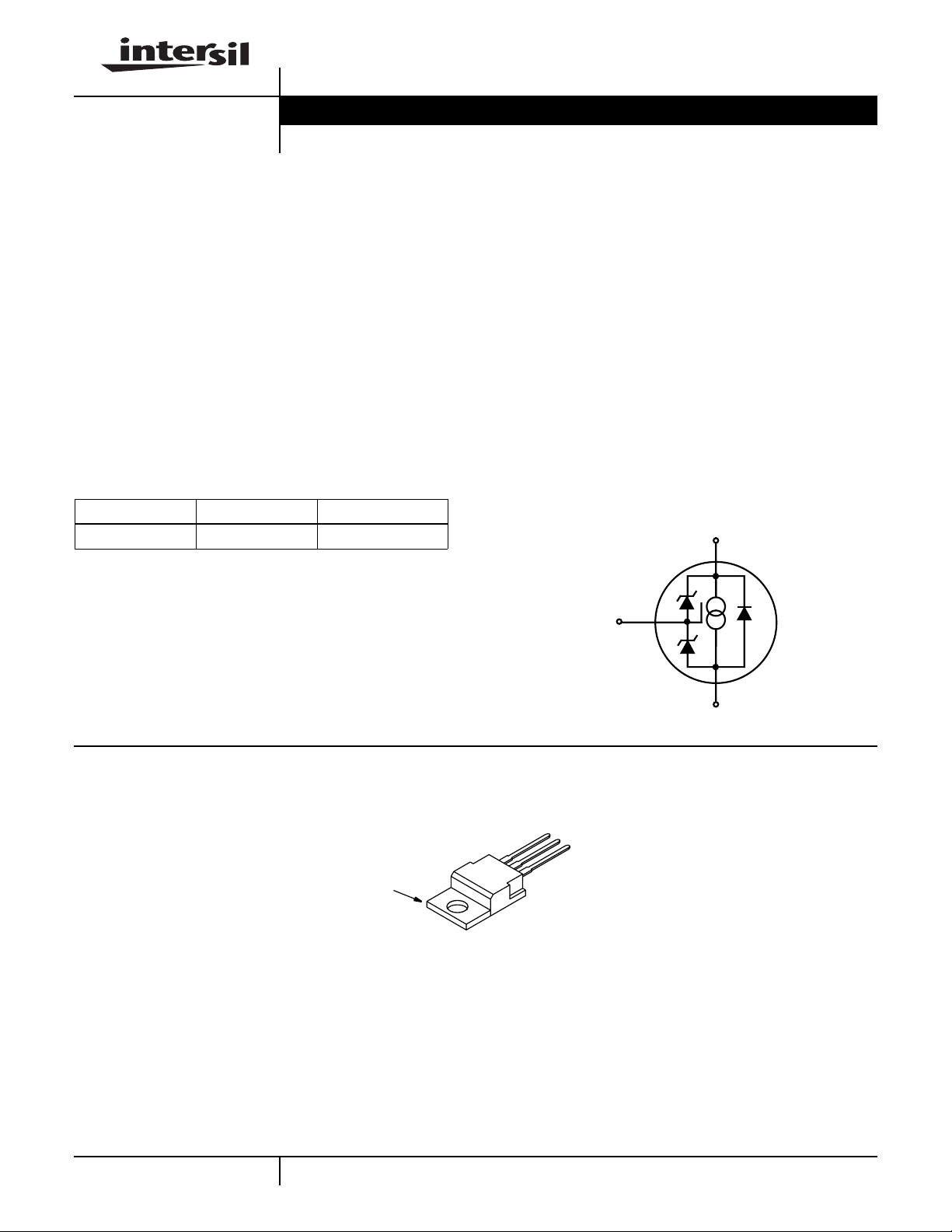
Symbol
D
2839.4
Packaging
G
S
JEDEC TO-220AB
SOURCE
DRAIN
GATE
DRAIN (FLANGE)
6-428
CAUTION: These devices are sensitive to electrostatic discharge; follow proper ESD Handling Procedures.
http://www.intersil.com or 407-727-9207
| Copyright © Intersil Corporation 1999

RLP1N06CLE
Absolute Maximum Ratings T
= 25oC, Unless Otherwise Specified
C
RLP1N06CLE UNITS
Drain to Source Voltage (Note 1). . . . . . . . . . . . . . . . . . . . . . . . . . . . . . . . . . . . . . . . . . . . .V
Drain to Gate Voltage (RGS = 20kΩ, Note 1). . . . . . . . . . . . . . . . . . . . . . . . . . . . . . . . . . . V
DSS
DGR
55 V
55 V
Electrostatic Voltage at TC = 25oC . . . . . . . . . . . . . . . . . . . . . . . . . . . . . . . . . . . . . . . . . . . ESD 2 kV
Continuous Drain Current . . . . . . . . . . . . . . . . . . . . . . . . . . . . . . . . . . . . . . . . . . . . . . . . . . . .I
Gate to Source Voltage (Reverse Voltage Gate Bias Not Allowed). . . . . . . . . . . . . . . . . . . .V
GS
Maximum Power Dissipation . . . . . . . . . . . . . . . . . . . . . . . . . . . . . . . . . . . . . . . . . . . . . . . . . .P
D
D
Self Limited
5.5 V
36 W
Power Dissipation Derating . . . . . . . . . . . . . . . . . . . . . . . . . . . . . . . . . . . . . . . . . . . . . . . . . . . . . 0.24 W/oC
Operating and Storage Temperature . . . . . . . . . . . . . . . . . . . . . . . . . . . . . . . . . . . . . . . TJ,T
STG
-55 to 175
Maximum Temperature for Soldering
Leads at 0.063in (1.6mm) from Case for 10s. . . . . . . . . . . . . . . . . . . . . . . . . . . . . . . . . . . . T
Package Body for 10s, See Techbrief 334 . . . . . . . . . . . . . . . . . . . . . . . . . . . . . . . . . . . . T
CAUTION: Stresses above those listed in “Absolute Maximum Ratings” may cause permanent damage to the device. This is a stress only rating and operationofthe
device at these or any other conditions above those indicated in the operational sections of this specification is not implied.
L
pkg
300
260
o
C
o
C
o
C
NOTE:
1. TJ= 25oC to 150oC.
Electrical Specifications T
= 25oC, Unless Otherwise Specified
C
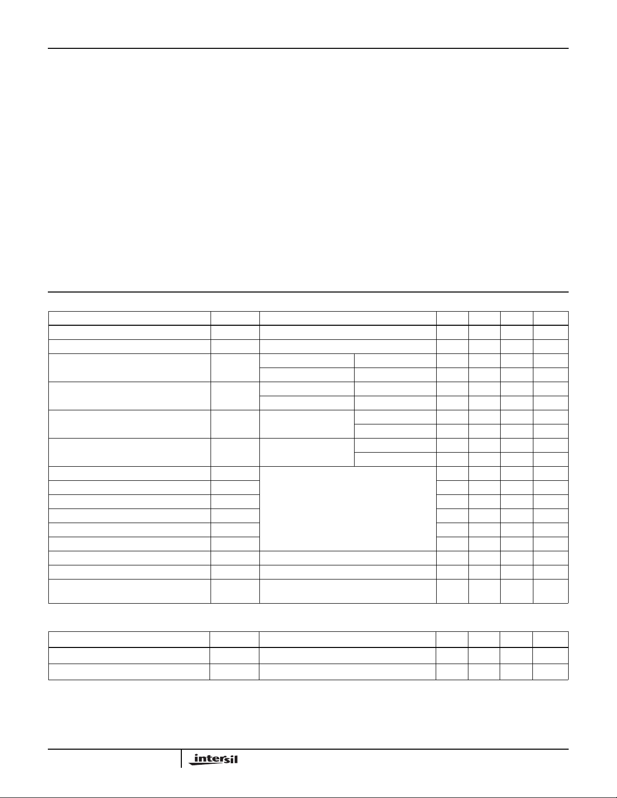
PARAMETER SYMBOL TEST CONDITIONS MIN TYP MAX UNITS
Drain to Source Breakdown Voltage BV
Gate to Threshold Voltage V
Zero Gate Voltage Drain Current I
DSSID
GS(TH)VGS
DSS
= 20mA, VGS = 0V (Figure 7) 55 - 70 V
= VDS, ID = 250µA (Figure 8) 1 - 2.5 V
VDS = 45V, VGS = 0V TC = 25oC--5µA
TC = 150oC--20µA
Gate to Source Leakage Current I
GSS
VGS = 5V TC = 25oC--5µA
TC = 150oC--20µA
Drain to Source On Resistance (Note 2) r
Limiting Current I
Turn-On Time t
Turn-On Delay Time t
Rise Time t
Turn-Off Delay Time t
Fall Time t
Turn-Off Time t
Thermal Resistance Junction to Case R
Thermal Resistance Junction to Ambient R
DS(ON)ID
DS(LIM)VDS
(ON)
d(ON)
r
d(OFF)
f
(OFF)
θJC
θJA
Electrostatic Voltage ESD Human Model (100pF, 1.5kΩ)
= 1A, VGS = 5V
(Figure 6)
= 15V, VGS = 5V
(Figure 2)
VDD = 30V, ID = 1A, VGS = 5V, RGS = 25Ω
RL = 30Ω
TC = 25oC - - 0.750 Ω
TC = 150oC - - 1.500 Ω
TC = 25oC 1.8 - 3 A
TC = 150oC 0.9 - 1.5 A
- - 6.5 µs
- - 1.5 µs
1-5µs
- - 7.5 µs
1-5µs
- - 12.5 µs
- - 4.17oC/W
TO-220AA - - 62
2000 - - V
o
C/W
MIL-STD-883B (Category B2)
Source to Drain Diode Specifications
PARAMETER SYMBOL TEST CONDITIONS MIN TYP MAX UNITS
Source to Drain Diode Voltage (Note 2) V
SD
Reverse Recovery Time t
NOTES:
2. Pulsed: pulse duration = 80µs maximum, duty cycle = 2%.
3. Repetitive rating: pulse width limited by maximum junction temperature.
6-429
ISD = 1A - - 1.5 V
ISD = 1A - - 1 ms
rr

RLP1N06CLE
Typical Performance Curves
1.2
1.0
0.8
0.6
0.4
0.2
POWER DISSIPATION MULTIPLIER
0
0 25 50 75 100 175
TC, CASE TEMPERATURE (oC)
Unless Otherwise Specified
125
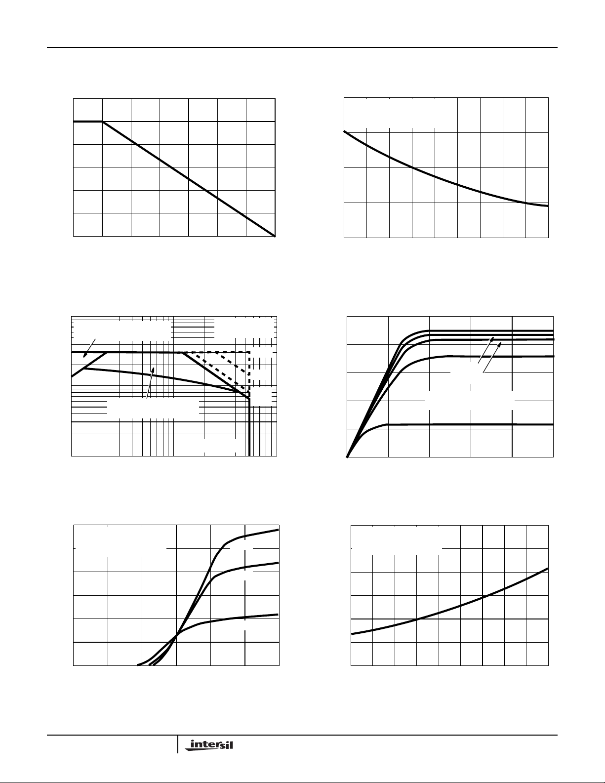
FIGURE 1. NORMALIZED POWER DISSIPATION vs CASE
TEMPERATURE
10
OPERATION IN THIS AREA
MAY BE LIMITED BY r
1
OPERATION IN THIS AREA
LIMITED BY I
, DRAIN TO SOURCE CURRENT (A)
DS
I
0.1
1 10 100
V
DS
DS(ON)
DS(LIM)
V
, DRAIN TO SOURCE VOLTAGE (V)
DSS
MAX = 55V
TJ = MAX RATED
T
= 25oC
C
150
100µs
1ms
10ms
DC
2.0
PULSE DURATION = 80µs
DUTY CYCLE = 0.5% MAX
= 10V, VGS = 5V
V
DS
1.5
1.0
0.5
NORMALIZED DRAIN CURRENT
0
-50 -25 0 25 50 75 100 125 150 175
T
, CASE TEMPERATURE (oC)
C
FIGURE 2. NORMALIZED CURRENT LIMIT vs CASE
TEMPERATURE
2.5
2.0
1.5
1.0
0.5
, DRAIN TO SOURCE CURRENT (A)
DS
I
0
012345
, DRAIN TO SOURCE VOLTAGE (V)
V
DS
VGS = 6V
= 5V
V
GS
PULSE DURATION = 80µs
DUTY CYCLE = 0.5% MAX
VGS = 7V
VGS = 4V
VGS = 3V
FIGURE 3. FORWARD BIAS SAFE OPERATING AREA FIGURE 4. SATURATION CHARACTERISTICS
3.0
VDS >> IDS x r
PULSE DURATION = 80µs
2.5
DUTY CYCLE = 0.5% MAX
2.0
1.5
1.0
, DRAIN TO SOURCE CURRENT (A)
0.5
DS(ON)
I
0
0123456
DS(ON)
, GATE TO SOURCE VOLTAGE (V)
V
GS
-25oC
25oC
150oC
3.0
VGS = 5V, ID = 0.5A
PULSE DURATION = 80µs
2.5
DUTY CYCLE = 0.5% MAX
2.0
1.5
1.0
ON RESISTANCE
0.5
NORMALIZED DRAIN TO SOURCE
0
-50 -25 0 25 50 75 100 125 150 175
, JUNCTION TEMPERATURE (oC)
T
J
FIGURE 5. TRANSFER CHARACTERISTICS FIGURE 6. NORMALIZED DRAIN TOSOURCE ON
RESISTANCE vs JUNCTION TEMPERATURE
6-430
 Loading...