Intersil RLD03N06CLE, RLD03N06CLESM, RLP03N06CLE Datasheet

RLD03N06CLE, RLD03N06CLESM,
RLP03N06CLE
Data Sheet July 1999
0.3A, 60V, 6 Ohm, ESD Rated, Current
Limited, Voltage Clamped, Logic Level
N-Channel Power MOSFETs
These are intelligent monolithic power circuits which
incorporate a lateral bipolar transistor, resistors, zener
diodes and a power MOS transistor. The current limiting of
these devices allow it to be used safely in circuits where a
shorted load condition may be encountered. The drain to
source voltage clamping offersprecisioncontrolofthecircuit
voltage when switching inductive loads. The “Logic Level”
gate allows this device to be fully biased on with only 5V
from gate to source, thereby facilitating true on-off power
control directly from logic level (5V) integrated circuits.
These devicesincorporate ESD protection andaredesigned
to withstand 2kV (Human Body Model) of ESD.
Formerly developmental type TA49028.
Ordering Information
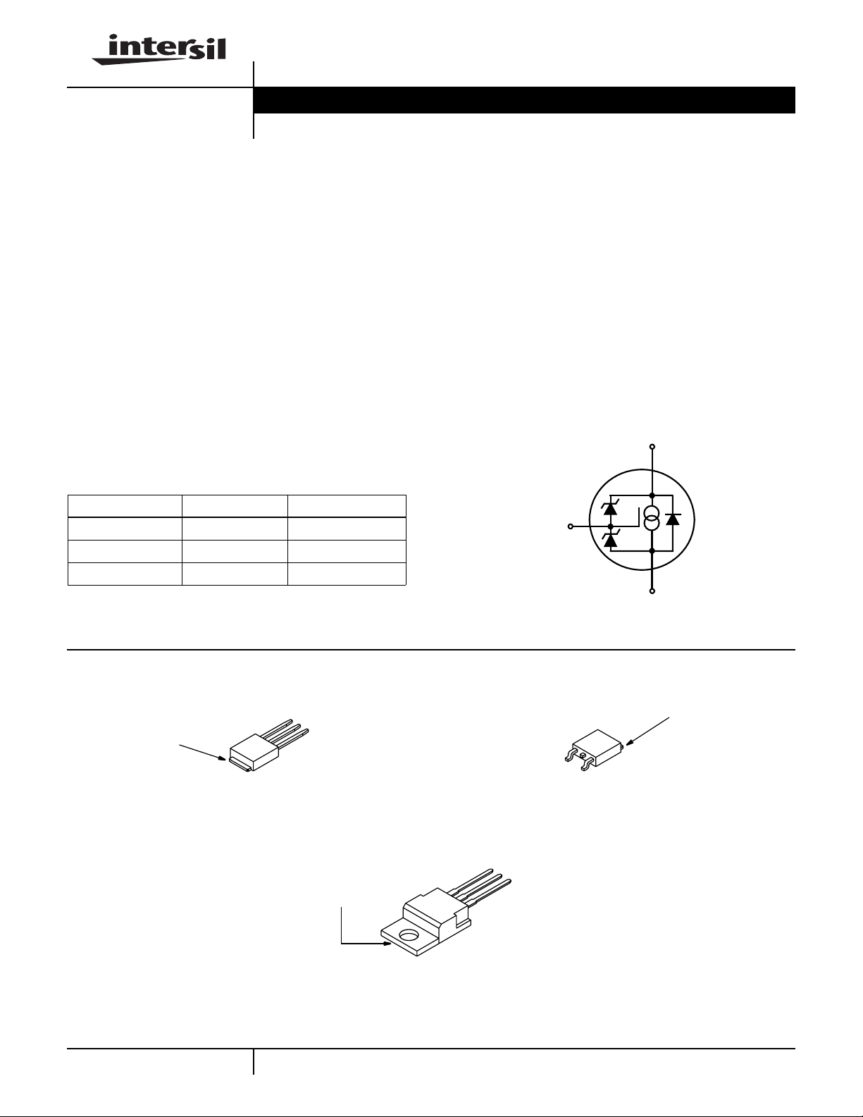
PART NUMBER PACKAGE BRAND
RLD03N06CLE TO-251AA 03N06C
RLD03N06CLESM TO-252AA 03N06C
RLP03N06CLE TO-220AB 03N06CLE
NOTE: Whenordering, usethe entire partnumber. Add the suffix9A to
obtainthe TO-252AAvariant in tape and reel,i.e. RLD03N06CLESM9A.
File Number
Features
• 0.30A, 60V
DS(ON)
= 6.0Ω
0.140 to 0.210A at 150oC
LIMIT
•r
• Built in Current Limit I
• Built in Voltage Clamp
®
• Temperature Compensating PSPICE
Model
• 2kV ESD Protected
• Controlled Switching Limits EMI and RFI
• Related Literature
- TB334 “Guidelines for Soldering Surface Mount
Components to PC Boards”
Symbol
D
G
S
3948.5
Packaging
(FLANGE)
DRAIN
JEDEC TO-251AA JEDEC TO-252AA
SOURCE
DRAIN
GATE
GATE
SOURCE
JEDEC TO-220AB
SOURCE
DRAIN
GATE
PSPICE® is a registered trademark of MicroSim Corporation.
| Copyright © Intersil Corporation 1999
6-418
DRAIN
(FLANGE)
CAUTION: These devices are sensitive to electrostatic discharge; follow proper ESD Handling Procedures.
http://www.intersil.com or 407-727-9207
DRAIN
(FLANGE)

RLD03N06CLE, RLD03N06CLESM, RLP03N06CLE
Absolute Maximum Ratings T
= 25oC, Unless Otherwise Specified
C
RLD03N06CLE, RLD03N06CLESM,
RLP03N06CLE UNITS
Drain to Source Voltage (Note 1). . . . . . . . . . . . . . . . . . . . . . . . . . . . . . . . . . . . .V
Drain to Gate Voltage. . . . . . . . . . . . . . . . . . . . . . . . . . . . . . . . . . . . . . . . . . . . . V
Gate to Source Voltage (Reverse Voltage Gate Bias Not Allowed). . . . . . . . . . . .V
Continuous Drain Current . . . . . . . . . . . . . . . . . . . . . . . . . . . . . . . . . . . . . . . . . . . . .I
Power Dissipation . . . . . . . . . . . . . . . . . . . . . . . . . . . . . . . . . . . . . . . . . . . . . . . . . . P
DSS
DGR
GS
D
D
Derate Above 25oC . . . . . . . . . . . . . . . . . . . . . . . . . . . . . . . . . . . . . . . . . . . . . . . . .
Electrostatic Discharge Rating MIL-STD-883, Category B(2) . . . . . . . . . . . . . . . .ESD 2 KV
Operating and Storage Temperature . . . . . . . . . . . . . . . . . . . . . . . . . . . . . . . TJ, T
STG
Maximum Temperature for Soldering
Leads at 0.063in (1.6mm) from Case for 10s. . . . . . . . . . . . . . . . . . . . . . . . . . . . T
Package Body for 10s, See Techbrief 334 . . . . . . . . . . . . . . . . . . . . . . . . . . . . .T
CAUTION: Stresses above those listed in “Absolute Maximum Ratings” may cause permanent damage to the device. This is a stress only rating and operationofthe
device at these or any other conditions above those indicated in the operational sections of this specification is not implied.
L
pkg
60 V
60 V
+5.5 V
Self Limited
30
0.2
-55 to 175
300
260
W
W/oC
o
C
o
C
o
C
NOTE:
1. TJ= 25oC to 150oC.
Electrical Specifications T
= 25oC, Unless Otherwise Specified
C
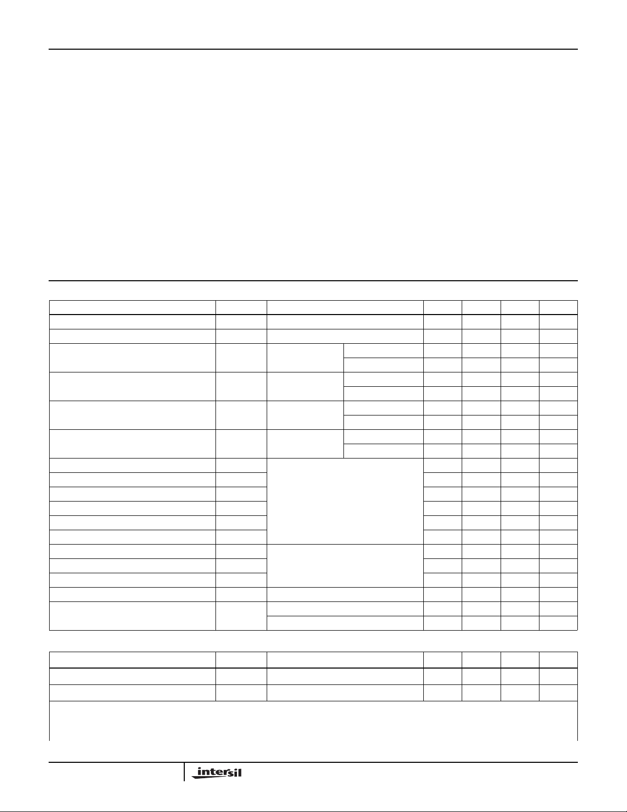
PARAMETER SYMBOL TEST CONDITIONS MIN TYP MAX UNITS
Drain to Source Breakdown Voltage BV
Gate Threshold Voltage V
Zero Gate Voltage Drain Current I
Gate to Source Leakage Current I
DSSID
GS(TH)VGS
DSS
GSS
= 250µA, VGS = 0V 60 - 85 V
= VDS, ID = 250µA 1 - 2.5 V
VDS = 45V,
VGS = 0V
TJ = 25oC--25µA
TJ = 150oC - - 250 µA
VGS = 5V TJ = 25oC--5µA
TJ = 150oC--20µA
Drain to Source On Resistance (Note 2) r
Limiting Current I
DS(ON)ID
DS(LIMIT)VDS
Turn-On Time t
Turn-On Delay Time t
d(ON)
Rise Time t
Turn-Off Delay Time t
d(OFF)
Fall Time t
Turn-Off Time t
Input Capacitance C
Output Capacitance C
Reverse Transfer Capacitance C
Thermal Resistance Junction to Case R
Thermal Resistance Junction to Ambient R
ON
r
f
OFF
ISS
OSS
RSS
θ
θ
JC
JA
= 0.100A,
VGS = 5V
= 15V,
VGS = 5V
VDD = 30V, ID = 0.10A,
RL = 300Ω, VGS = 5V,
RGS = 25Ω
TJ = 25oC - - 6.0 Ω
TJ = 150oC - - 12.0 Ω
TJ = 25oC 280 - 420 mA
TJ = 150oC 140 - 210 mA
- - 7.5 µs
- - 2.5 µs
- - 5.0 µs
- - 7.5 µs
- - 5.0 µs
- - 12.5 µs
VDS = 25V, VGS = 0V,
f = 1MHz
- 100 - pF
-65-pF
- 3.0 - pF
- - 5.0
TO-220 Package - - 80
TO-251 and TO-252 Packages - - 100
o
o
o
C/W
C/W
C/W
Source to Drain Diode Specifications
PARAMETER SYMBOL TEST CONDITIONS MIN TYP MAX UNITS
Source to Drain Diode Voltage V
SD
Diode Reverse Recovery Time t
NOTES:
2. Pulsed: pulse duration = ≤ 300µs maximum, duty cycle = ≤ 2%.
3. Repititive rating: pulse width limited by maximum junction temperature.
6-419
ISD = 0.1A - - 1.5 V
ISD = 0.1A, dISD/dt = 100A/µs - - 1.0 ms
rr

RLD03N06CLE, RLD03N06CLESM, RLP03N06CLE
Typical Performance Curves
1.2
1.0
0.8
0.6
0.4
0.2
POWER DISSIPATION MULTIPLIER
0
25 50 75 100 125 150 1750
0
TC, CASE TEMPERATURE (oC)
Unless Otherwise Specified
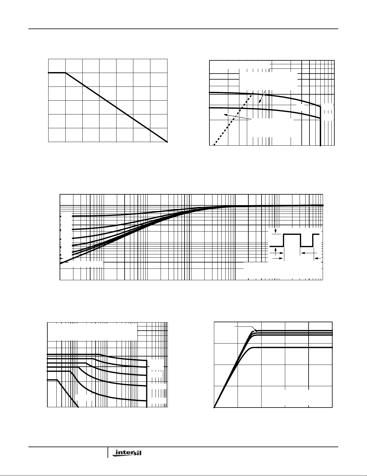
FIGURE 1. NORMALIZEDPOWER DISSIPATION vs CASE
TEMPERATURE
2
1
1
TC = 25oC, TJ = MAX RATED
OPERATION IN THIS
AREA IS LIMITED BY
JUNCTION TEMPERATURE
DC
, DRAIN CURRENT (A)
D
I
0.1
1 10 100
VDS, DRAIN TO SOURCE VOLTAGE (V)
OPERATION IN THIS
AREA MAY BE
LIMITED BY r
DS(ON)
FIGURE 2. FORWARD BIAS SAFE OPERATING AREA
25oC
175oC
0.5
0.2
0.1
0.1
, NORMALIZED
JC
θ
Z
1
, CLAMPED DRAIN CURRENT (A)
(CLAMP)
I
0.1
0.001
0.05
0.02
0.01
THERMAL IMPEDANCE
SINGLE PULSE
0.01
-5
10
= 25oC
T
C
TEMPERATURES LISTED ARE STARTING
JUNCTION TEMPERATURES
150oC
0.01 0.1 1 10
tAV, TIME IN CLAMP (s)
NOTES:
DUTY FACTOR: D = t1/t
PEAK TJ = PDM x Z
-4
10
-3
10
t, RECTANGULAR PULSE DURATION (s)
-2
10
-1
10
FIGURE 3. NORMALIZED MAXIMUM TRANSIENT THERMAL IMPEDANCE
0.40
VGS = 5V
0.30
25oC
50oC
75oC
100oC
125oC
0.20
, DRAIN CURRENT (A)
D
0.10
I
0
012345
VDS, DRAIN TO SOURCE VOLTAGE (V)
P
DM
t
1
t
2
2
x R
JC
θ
= 7.5V
+ T
JC
θ
0
10
V
GS
PULSE DURATION = 80µs
DUTY CYCLE = 0.5% MAX
= 25oC
T
C
C
10
= 4V
V
GS
VGS = 3V
1
FIGURE 4. SELF-CLAMPED INDUCTIVE SWITCHING FIGURE 5. SATURATION CHARACTERISTICS
6-420
 Loading...