

Intersil RFL1N10L, RFL1N08L Datasheet
1
Features
• 1A, 100V
•r
DS(ON)
= 1.200Ω
Description
This is an N-Channel enhancement mode silicon gate power
field effect transistor specifically designed for use with logic
level (5V) driving sources in applications such as programmable controllers, automotive switching, and solenoid drivers. This performance is accomplished through a special
gate oxide design which provides full rated conduction at
gate biases in the 3V to 5V range, thereby facilitating true
on-off power control directly from logic circuit supply voltages.
Formerly developmental type TA09524.
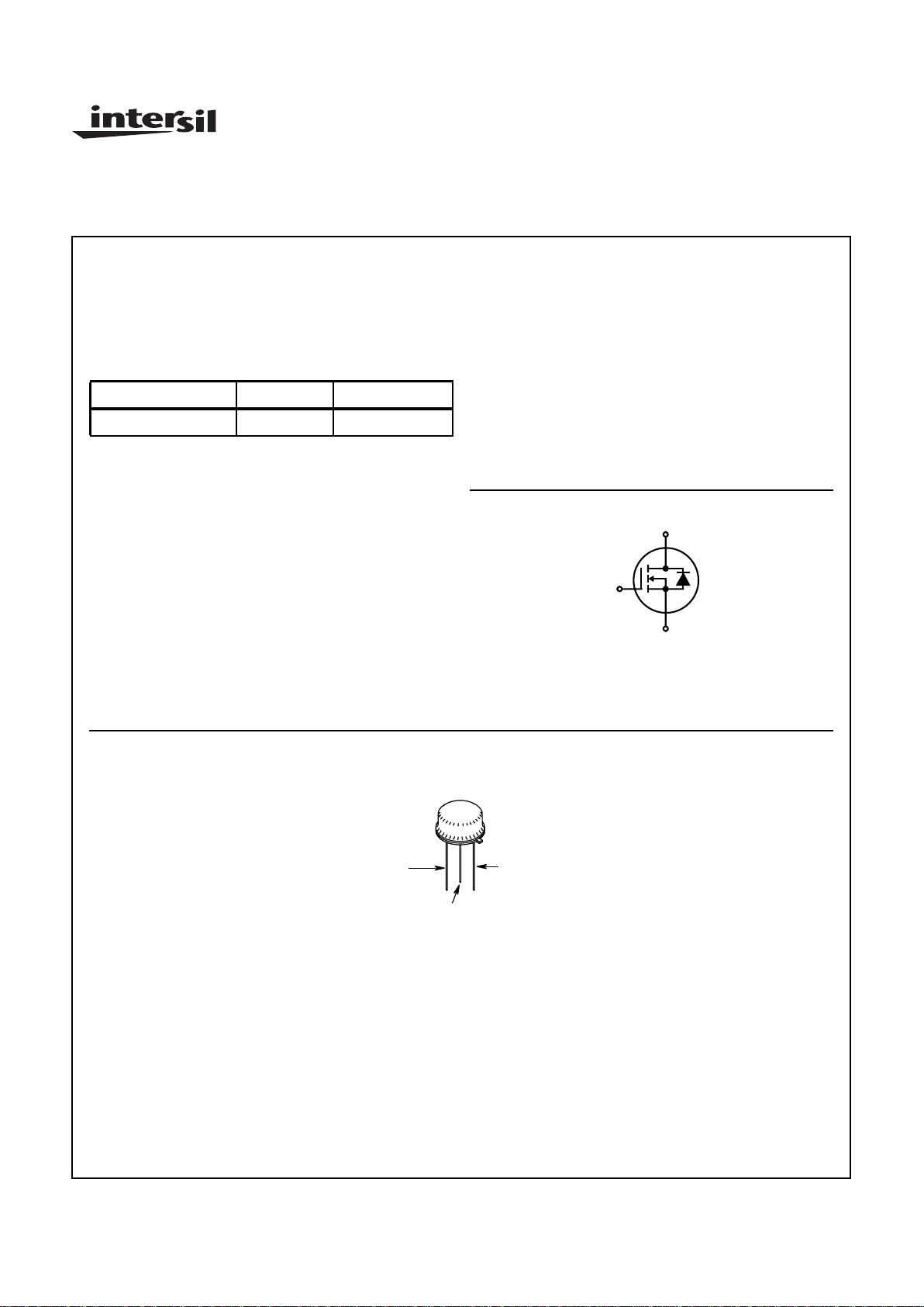
Symbol
Packaging
JEDEC TO-205AF
Ordering Information
PART NUMBER PACKAGE BRAND
RFL1N10L TO-205AF RFL1N10L
NOTE: When ordering, use the entire part number.
G
D
S
DRAIN
(CASE)
SOURCE
GATE
September 1998
File Number
1510.3
RFL1N10L
1A, 100V, 1.200 Ohm, Logic Level, N-Channel
Power MOSFET
CAUTION: These devices are sensitive to electrostatic discharge; follow proper ESD Handling Procedures.
http://www.intersil.com or 407-727-9207
| Copyright © Intersil Corporation 1999

2
Absolute Maximum Ratings T
C
= 25oC, Unless Otherwise Specified
RFL1N10L UNITS
Drain to Source Voltage (Note 1) . . . . . . . . . . . . . . . . . . . . . . . . . . . . . . . . V
DS
100 V
Drain to Gate Voltage (RGS = 1MΩ) (Note 1). . . . . . . . . . . . . . . . . . . . . .V
DGR
100 V
Continuous Drain Current. . . . . . . . . . . . . . . . . . . . . . . . . . . . . . . . . . . . . . . . I
D
1A
Pulsed Drain Current (Note 3) . . . . . . . . . . . . . . . . . . . . . . . . . . . . . . . . .I
DM
5A
Gate to Source Voltage . . . . . . . . . . . . . . . . . . . . . . . . . . . . . . . . . . . . . . . V
GS
±10 V
Maximum Power Dissipation . . . . . . . . . . . . . . . . . . . . . . . . . . . . . . . . . . . . P
D
8.33 W
Above TC = 25oC, Derate Linearly . . . . . . . . . . . . . . . . . . . . . . . . . . . . . . . . . 0.0667 W/oC
Operating and Storage Temperature . . . . . . . . . . . . . . . . . . . . . . . . . TJ, T
STG
-55 to 150
o
C
Maximum Temperature for Soldering
Leads at 0.063in (1.6mm) from Case for 10s . . . . . . . . . . . . . . . . . . . . . . .T
L
260
o
C
CAUTION: Stresses above those listed in “Absolute Maximum Ratings” may cause permanent damage to the device. This is a stress only rating and operation
of the device at these or any other conditions above those indicated in the operational sections of this specification is not implied.
NOTE:
1. TJ= 25oC to 125oC.
Electrical Specifications T
C
= 25oC, Unless Otherwise Specified
PARAMETER SYMBOL TEST CONDITIONS MIN TYP MAX UNITS
Drain to Source Breakdown Voltage BV
DSS
ID = 250µA, VGS = 0 100 - - V
Gate Threshold Voltage V
GS(TH)
VGS = VDS, ID = 250µA1-2V
Zero Gate Voltage Drain Current I
DSS
VDS = Rated BV
DSS
--1µA
VDS = 0.8 x Rated BV
DSS
, VDS = 80V,
TC = 125oC
--25µA
Gate to Source Leakage Current I
GSS
VGS = ±10V, VDS = 0 - - ±100 nA
Drain to Source On Resistance (Note 2) r
DS(ON)
ID = 1A, VGS = 5V (Figures 6, 7) - - 1.200 Ω
Drain to Source On Voltage (Note 2) V
DS(ON)
ID = 1A, VGS = 5V - - 1.2 V
Turn-On Delay Time t
d(ON)
I
D
≈ 1A, V
DD
= 50V, RG= 6.25Ω,
VGS = 5V, RL= 50Ω
(Figures 10, 11, 12)
-1025ns
Rise Time t
r
-1545ns
Turn-Off Delay Time t
d(OFF)
-2545ns
Fall Time t
f
-3050ns
Input Capacitance C
ISS
VGS = 0V, VDS = 25V, f = 1MHz
(Figure 9)
- - 200 pF
Output Capacitance C
OSS
- - 80 pF
Reverse Transfer Capacitance C
RSS
- - 35 pF
Thermal Resistance Junction to Case R
θ
JC
--15oC/W
Source to Drain Diode Specifications
PARAMETER SYMBOL TEST CONDITIONS MIN TYP MAX UNITS
Source to Drain Diode Voltage (Note 2) V
SD
ISD = 1A - - 1.4 V
Diode Reverse Recovery Time t
rr
ISD = 2A, dISD/dt = 50A/µs - 100 - ns
NOTES:
2. Pulse test: width ≤ 300µs duty cycle ≤ 2%.
3. Repetitive rating: pulse witdh limited by maximum junction temperature.
RFL1N10L
 Loading...