

Intersil RFH10N45, RFH10N50 Datasheet
Semiconductor
/
/
/
/
/
RFH10N45, RFH10N50
Data Sheet October 1998 File Number 1629.2
[ /Title
(RFH10
N45,
RFH10N
50)
Subject
(10A,
450V
and
500V,
0.600
Ohm,
N-Channel
Power
MOSFETs)
Author
()
Key-
words
(Harris
Semiconductor,
N-Channel
Power
MOSFETs,
TO218AC)
Creator
()
DOCIN
FO pdfmark
10A, 450V and 500V, 0.600 Ohm,
N-Channel Power MOSFETs
These are N-Channel enhancement mode silicon gate
power field effect transistors designed for applications such
as switching regulators, switching converters, motor drivers,
relay drivers, and drivers for high power bipolar switching
transistors requiring high speed and low gate drive power.
These types can be operated directly from integrated circuits.
Formerly developmental type TA17435.
Ordering Information
PART NUMBER PACKAGE BRAND
RFH10N45 TO-218AC RFH10N45
RFH10N50 TO-218AC RFH10N50
NOTE: When ordering, include the entire part number.
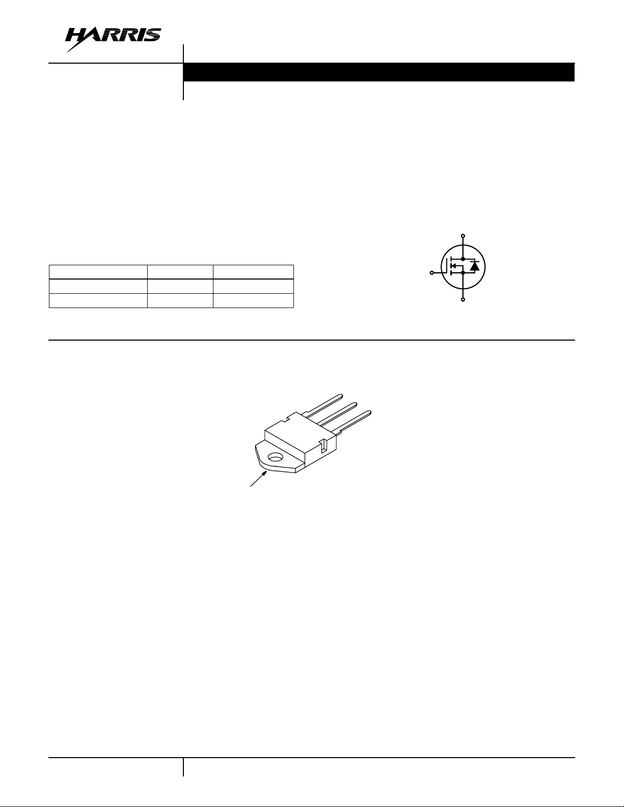
Packaging
JEDEC TO-218AC
DRAIN
(FLANGE)
Features
• 10A, 450V and 500V
•r
DS(ON)
• Related Literature
- TB334 “Guidelines for Soldering Surface Mount
= 0.600Ω
Components to PC Boards”
Symbol
D
G
S
SOURCE
DRAIN
GATE
1
CAUTION: These devices are sensitive to electrostatic discharge; follow proper IC Handling Procedures.
1-800-4-HARRIS
| Copyright © Harris Corporation 1998
RFH10N45, RFH10N50S
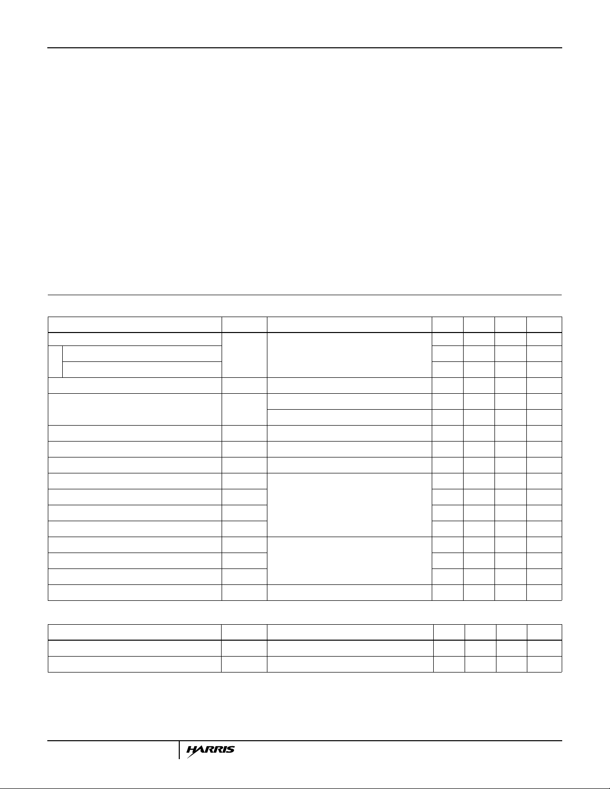
Absolute Maximum Ratings T
= 25oC, Unless Otherwise Specified
C
RFH10N45 RFH10N50 UNITS
Drain to Source Voltage (Note 1). . . . . . . . . . . . . . . . . . . . . . . . . . . . . . . V
Drain to Gate Voltage (RGS = 1MΩ) (Note 1) . . . . . . . . . . . . . . . . . . . . . V
DSS
DGR
Continuous Drain Current . . . . . . . . . . . . . . . . . . . . . . . . . . . . . . . . . . . . . . . I
Pulsed Drain Current (Note 3) . . . . . . . . . . . . . . . . . . . . . . . . . . . . . . . . . . . I
Gate to Source Voltage . . . . . . . . . . . . . . . . . . . . . . . . . . . . . . . . . . . . . . . V
Maximum Power Dissipation . . . . . . . . . . . . . . . . . . . . . . . . . . . . . . . . . . . . P
D
DM
GS
D
450 500 V
450 500 V
10 10 A
20 20 A
±20 ±20 V
150 150 W
Linear Derating Factor. . . . . . . . . . . . . . . . . . . . . . . . . . . . . . . . . . . . . . . . . . . . 1.2 1.2 W/oC
Operating and Storage Temperature . . . . . . . . . . . . . . . . . . . . . . . . TJ, T
STG
-55 to 150 -55 to 150
Maximum Temperature for Soldering
Leads at 0.063in (1.6mm) from Case for 10s. . . . . . . . . . . . . . . . . . . . . . . T
Package Body for 10s, See TB334. . . . . . . . . . . . . . . . . . . . . . . . . . . . . T
CAUTION: Stresses above those listed in “Absolute Maximum Ratings” may cause permanent damage to the device. This is a stress only rating and operationofthe
device at these or any other conditions above those indicated in the operational sections of this specification is not implied.
L
pkg
300
260
300
260
o
C
o
C
o
C
NOTE:
1. TJ= 25oC to 125oC.
Electrical Specifications T
= 25oC, Unless Otherwise Specified
C
PARAMETER SYMBOL TEST CONDITIONS MIN TYP MAX UNITS
Drain to Source Breakdown Voltage BV
DSSID
= 250µA, VGS = 0V
RFH10N45 450 V
RFH10N50 500 V
Gate to Threshold Voltage V
GS(TH)VGS
Zero-Gate Voltage Drain Current I
Gate to Source Leakage Current I
Drain to Source On Voltage (Note 2) V
Drain to Source On Resistance (Note 2) r
Turn-On Delay Time t
DS(ON)ID
DS(ON)ID
d(ON)ID
Rise Time t
Turn-Off Delay Time t
d(OFF)
Fall Time t
Input Capacitance C
Output Capacitance C
Reverse Transfer Capacitance C
Thermal Resistance, Junction to Case R
DSS
GSS
r
f
ISS
OSS
RSS
JC
θ
= VDS, ID = 250µA (Figure 8) 2 - 4 V
VDS= Rated BV
DSS
VDS= 0.8 x Rated BV
TC = 125oC--25µA
DSS,
--1µA
VGS = ±20V, VDS = 0V - - ±100 nA
= 10A, VGS = 10V - - 6.0 V
= 10A, VGS = 10V (Figures 6, 7) - - 0.600 Ω
≈ 5A, V
R
= 50Ω, V
L
(Figures 10, 11, 12)
= 250V, R
DS
= 10V
GS
= 50Ω,
G
-2660ns
- 50 100 ns
- 525 900 ns
- 105 180 ns
VGS = 0V, VDS = 25V
f = 1MHz (Figure 9)
- - 3000 pF
- - 600 pF
- - 200 pF
- - 0.83oC/W
Source to Drain Diode Specifications
PARAMETER SYMBOL TEST CONDITIONS MIN TYP MAX UNITS
Source to Drain Diode Voltage (Note 2) V
Diode Reverse Recovery Time t
NOTES:
2. Pulse Test: Pulse Width ≤ 300µs, Duty Cycle ≤ 2%.
3. Repetitive rating: pulse width is limited by maximum junction temperature.
2
ISD = 10A - - 1.4 V
SD
ISD = 10A, dISD/dt = 100A/µs - 950 - ns
rr
 Loading...