

Intersil RFG75N05E Datasheet
RFG75N05E
75A, 50V, 0.008 Ohm, N-Channel Power
MOSFET
These are N-Channel enhancement mode silicon gate
power field effect transistors. They are advanced power
MOSFETs designed, tested, and guaranteed to withstand a
specified level of energy in the breakdown avalanche mode
of operation. All of these power MOSFETs are designed for
applications such as switching regulators, switching
convertors, motor drivers, relay drivers, and drivers for high
power bipolar switching transistors requiring high speed and
low gate drive power. These types can be operated directly
from integrated circuits.
Formerly developmental type TA09821.
Ordering Information
PART NUMBER PACKAGE BRAND
RFG75N05E TO-247 RFG75N05E
NOTE: When ordering, include the entire part number.
July 1999Data Sheet File Number
Features
• 75A, 50V
DS(ON)
= 0.008Ω
•r
• Electrostatic Discharge Rated
• UIS Rating Curve (Single Pulse)
o
C Operating Temperature
• 175
• Temperature Compensated PSPICE
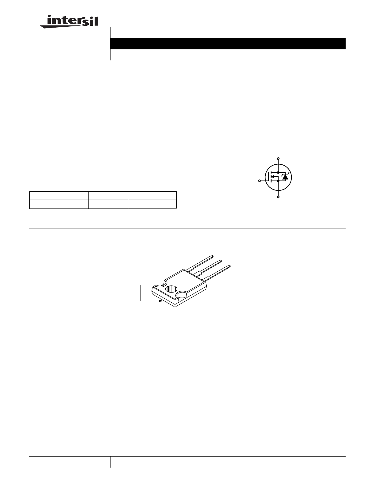
Symbol
D
G
S
2275.5
®
Model Provided
Packaging
DRAIN
(BOTTOM
SIDE METAL)
JEDEC STYLE TO-247
SOURCE
DRAIN
GATE
4-481
CAUTION: These devices are sensitive to electrostatic discharge; follow proper ESD Handling Procedures.
PSPICE® is a registered trademark of MicroSim Corporation.
http://www.intersil.com or 407-727-9207
| Copyright © Intersil Corporation 1999
RFG75N05E
Absolute Maximum Ratings T
= 25oC, Unless Otherwise Specified
C
RFG75N05E UNITS
Drain to Source Voltage (Note 1). . . . . . . . . . . . . . . . . . . . . . . . . . . . . . . . . . . . . . . . . . . . . . . . . . . .V
Drain to Gate Voltage (RGS = 20kΩ) (Note 1) . . . . . . . . . . . . . . . . . . . . . . . . . . . . . . . . . . . . . . . . . V
DSS
DGR
Continuous Drain Current (Current Limited by Package). . . . . . . . . . . . . . . . . . . . . . . . . . . . . . . . . . . . I
Pulsed Drain Current (Note 3) . . . . . . . . . . . . . . . . . . . . . . . . . . . . . . . . . . . . . . . . . . . . . . . . . . . . . . . I
Gate to Source Voltage . . . . . . . . . . . . . . . . . . . . . . . . . . . . . . . . . . . . . . . . . . . . . . . . . . . . . . . . . . . .V
Maximum Power Dissipation . . . . . . . . . . . . . . . . . . . . . . . . . . . . . . . . . . . . . . . . . . . . . . . . . . . . . . . . .P
D
DM
GS
D
50 V
50 V
75 A
200 A
±20 V
240 W
Linear Derating Factor. . . . . . . . . . . . . . . . . . . . . . . . . . . . . . . . . . . . . . . . . . . . . . . . . . . . . . . . . . . . . . . . 1.6 W/oC
Electrostatic Discharge Rating, MIL-STD-883, Category B(2). . . . . . . . . . . . . . . . . . . . . . . . . . . . . . E
SD
2kV
Single Pulse Avalanche Rating (Note 4) . . . . . . . . . . . . . . . . . . . . . . . . . . . . . . . . . . . . . . . . . . . . . . . . . . Refer to UIS SOA
Curves
Operating and Storage Temperature . . . . . . . . . . . . . . . . . . . . . . . . . . . . . . . . . . . . . . . . . . . . . TJ, T
STG
-55 to 175
Maximum Temperature for Soldering
Leads at 0.063in (1.6mm) from Case for 10s. . . . . . . . . . . . . . . . . . . . . . . . . . . . . . . . . . . . . . . . . . . T
Package Body for 10s, See Techbrief 334 . . . . . . . . . . . . . . . . . . . . . . . . . . . . . . . . . . . . . . . . . . . T
CAUTION: Stresses above those listed in “Absolute Maximum Ratings” may cause permanent damage to the device. This is a stress only rating and operationofthe
device at these or any other conditions above those indicated in the operational sections of this specification is not implied.
L
pkg
300
260
o
C
o
C
o
C
NOTE:
1. TJ= 25oC to 125oC.
Electrical Specifications T
= 25oC, Unless Otherwise Specified
C
PARAMETER SYMBOL TEST CONDITIONS MIN TYP MAX UNITS
Drain to Source Breakdown Voltage BV
Gate Threshold Voltage V
GS(TH)VGS
Zero Gate Voltage Drain Current I
Gate to Source Leakage I
Drain to Source on Resistance (Note 2) r
DS(ON)VGS
Turn On Time t
Turn On Delay Time t
d(ON)
Rise Time t
Turn Off Delay Time t
d(OFF)
Fall Time t
Turn Off Time t
Total Gate Charge
(OFF)
Q
g(TOT)VGS
(Gate to Source + Gate to Drain)
Gate Charge at 10V Q
Threshold Gate Charge Q
Junction to Case R
Junction to Ambient R
DSSVGS
DSS
GSS
(ON)
r
f
g(10)
g(TH)VGS
θJC
θJA
= 0V, ID = 250µA (Figure 9) 50 - - V
= VDS, ID = 250µA (Figure 8) 2.0 - 4.0 V
VDS = Rated BV
VDS = 0.8 x Rated BV
, VGS = 0V - - 1 µA
DSS
, VGS = 0V, TC = 150oC- -25µA
DSS
VGS = ±20V - - ±100 nA
= 10V, ID = 75A (Figure 7) - - 0.008 Ω
VDD= 25V, I
RL = 0.67Ω, RG= 1.67Ω, VGS = 10V,
(Figure 11)
≈ 37.5A,
D
- - 125 ns
-17- ns
-75- ns
-70- ns
-17- ns
- - 125 ns
= 0, 20V VDD = 40V, ID = 75A,
- - 400 nC
RL = 0.53Ω
I
= 3.44mA
VGS = 0, 10V - - 220 nC
G(REF)
(Figure 11)
= 0, 2V - - 15 nC
- - 0.625oC/W
--80oC/W
Source to Drain Diode Specifications
PARAMETER SYMBOL TEST CONDITIONS MIN TYP MAX UNITS
Source to Drain Diode Voltage V
Diode Reverse Recovery Time t
NOTES:
2. Pulse test: pulse width ≤ 300µs, duty cycle ≤ 2%.
3. Repetitive pulse: pulse width is limited by maximum junction temperature.
4. Refer to Intersil Application Notes AN9321 and AN9322. See Figure 4.
4-482
ISD= 75A - - 1.5 V
SD
ISD = 75A, dISD/dt = 100A/µs - - 125 ns
rr
 Loading...