®
www.BDTIC.com/Intersil
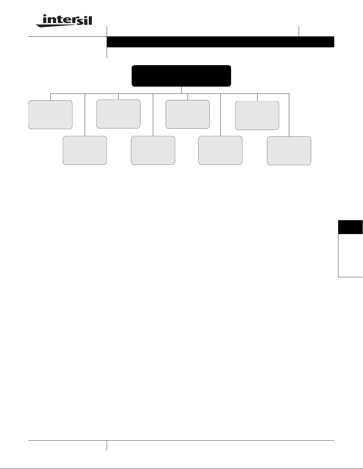
Power Management
2008 PRODUCT SELECTION GUIDE
Power Management
(pg. 10-1)
10
Battery
Management
(pg. 10-2)
Hot Plug
Controllers
(pg. 10-6)
Isolated Power
(pg. 10-8)
LNB Controllers
(pg. 10-9)
Linear
Regulation
(pg. 10-10)
Power MOSFET
Drivers
(pg. 10-11)
Power Supply
Support
(pg. 10-15)
Switching
Regulation
(pg. 10-21)
10
Power
Management
10-1
1-888-INTERSIL or 1-888-468-3774 | Copyright © 2008 Intersil Americas Inc. All rights reserved.
www.intersil.com
www.intersil.com/power/
www.BDTIC.com/Intersil
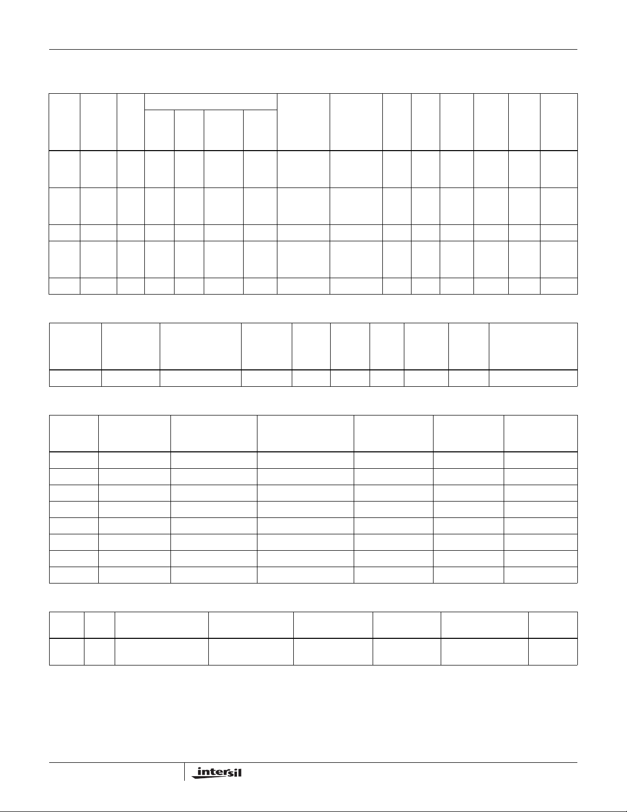
Battery Management
Cell Balancing and Safety
# of
Series
Connected
Li-Ion
Device
ISL9208 4 to 7 Y Y Y Discharge +
ISL9216 5 Y Y Y Discharge +
ISL9217 4 to 7 N Y Y N N N N Y N Y 3.3 I
ISL94200 4 to 7 Y Y Y Discharge +
ISL94201 4 to 7 N Y Y N N N N Y N N 3.3 I
Cells
Power
FET
Control
Over-
voltage
Under-
voltage
Shutdown
Over-
current
Charge
Charge
Charge
Programmable
Short
Circuit
Discharge 4-Discharge OC,
Discharge 4-Discharge OC,
Discharge 4-Discharge OC,
Threshold
4-Charge OC,
4-Short Circuit
4-Charge OC,
4-Short Circuit
4-Charge OC,
4-Short Circuit
Programmable
Timeout
8-Discharge OC,
8-Charge OC,
2-Short Circuit
8-Discharge OC,
8-Charge OC,
2-Short Circuit
8-Discharge OC,
8-Charge OC,
2-Short Circuit
Cell
Pack
Voltage
Current
Monitor
Monitor
YN Y 3.3I
YN Y 3.3I
YY N 3.3I
Cell
Balancing
FETs
Voltage
Regulator
(V) Interface Package
2
C Eval Board,
32 Ld QFN
2
C Eval Board,
32 Ld QFN
2
C 24 Ld QFN
2
C 24 Ld QFN
2
C 24 Ld QFN
Battery Status Monitors and Backup Switches
System Management:
System Resets,
Device
ICL7673 N/A Yes Yes 2.5 15 5 38 50 8 Ld PDIP, 8 Ld SOIC
# of Li-Ion
Cells Protected
Power Indicators,
Fault Detection
Over-Charge
Protection
V
IN
(min)
(V)
V
IN
(max)
(V)
I
S
(max)
(A)
I
OUT
(max)
(mA)
Input Trip
(mV) Package
Charge System Safety
Programmable
Overcurrent
Device
ISL9200 0 to 1 6.8 typ, 6.65 min, 7.0 max 4.4 typ, 4.325 min, 4.475 max 20nA max @ 4.4VVB 250 typ, 450 max 12 Ld QFN
ISL9209 0 to 1 5.58 typ, 5.65 min, 6.0 max 4.4 typ, 4.32 5 min, 4.475 max 20nA max @ 4.4VVB 250 typ, 450 max 12 Ld DFN
ISL9209B 0 to 1.5 5.58 typ, 5.65 min, 6.0 max 4.34 typ, 4.28 min, 4.4 max 20nA max @ 4.34VVB 250 typ, 450 max 12 Ld TDFN
ISL9209C 0 to 1.5 5.58 typ, 5.65 min, 6.0 max 4.34 typ, 4.28 min, 4.4 max 20nA max @ 4.4VVB 170 typ, 280 max 12 Ld TDFN
ISL9211 0 to 1.5 5.8 typ, 5.6 min, 6.0 max 4.34 typ, 4.25 min, 4.4 max 20nA max @ 4.4VVB 170 typ, 280 max 8 Ld TDFN T+R
ISL9212 0 to 2 6.8 typ, 6.65 min, 7.0 max 4.4 typ, 4.325 min, 4.475 max 20nA max @ 4.4VVB 170 typ, 280 max 12 Ld DFN
ISL9212A 0 to 2 6.8 typ, 6.65 min, 7.0 max 4.4 typ, 4.325 min, 4.475 max 20nA max @ 4.4VVB 170 typ, 280 max 12 Ld DFN
ISL9212B 0 to 2 6.8 typ, 6.65 min, 7.0 max 4.4 typ, 4.325 min, 4.475 max 20nA max @ 4.4VVB 170 typ, 280 max 12 Ld DFN
(A)
Input Overvoltage
Protection
(V)
Battery Overvoltage
Protection
(V) Battery Leakage
@ 500mA
R
ON
(mΩ) Package
Fuel Gauges
V
Operating Temp. Range
Device
ISL6295 2.8 to 7 -20 to 85 400 85 15 Bits + Sign 256 Bytes of EEPROM,
(V)
S
(°C)
Supply Current Sleep
(nA)
Supply Current Run
(µA)
A/D
Measurement Comments Package
8 Ld TSSOP
Temp measurement
10-2
1-888-INTERSIL or 1-888-468-3774 | Copyright © 2008 Intersil Americas Inc. All rights reserved.
www.intersil.com
www.intersil.com/power/
www.BDTIC.com/Intersil
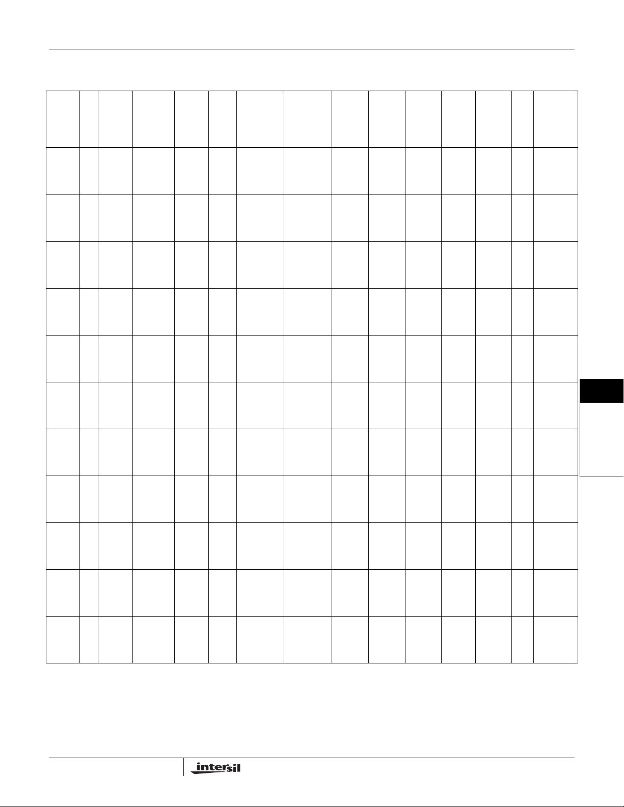
Multiple Cell Li+/Polymer Battery Charger
Input Voltage Range: 7V to 25V, Topology: Fixed Freq uency Synchronous Buck, Audible Noise: No, Operating Temperature Range: -10°C to 100°C, Thermal Shutdown: +150°C
Input
Current
Limit
Accuracy
Device iSim
ISL6251 Y ±3 4.2/Cell
ISL6251A Y ±3 4.2/Cell
ISL6252 ±3 4.2/Cell
ISL6252A ±3 4.2/Cell
ISL6256 ±3 4.2/Cell
ISL6256A ±3 4.2/Cell
ISL6253 ±3 4.2/Cell
ISL6255 Y ±3 4.2/Cell
ISL6255A Y ±3 4.2/Cell
ISL6257 ±1.5 4.2/Cell
ISL6258 ±3 6.144 to
(%)
Battery
Charge
Voltage
(2S, 3S, 4S)
(2S, 3S, 4S)
(2S, 3S, 4S)
(2S, 3S, 4S)
(2S, 3S, 4S)
(2S, 3S, 4S)
(2S, 3S, 4S)
(2S, 3S, 4S)
(2S, 3S, 4S)
(2S, 3S, 4S)
19.2 in
16mV Steps
(V)
Charging
Voltage
Accuracy
Battery
Charge
Voltage
(max)
(%)
±0.5 ±5/Cell ±5
±0.5 ±5/Cell ±3
±0.5 ±5/Cell ±3
±0.5 ±5/Cell ±3
±0.5 ±5/Cell ±3
±0.5 ±5/Cell ±3
±0.6 ±5/Cell ±3
±0.5 ±5/Cell ±5
±0.5 ±5/Cell ±3
±0.5 ±5/Cell ±1.5
±0.5 16mV
Current Limit
Adjust
(%)
(CHLIM=2.0V)
(CHLIM=2.0V)
(CHLIM=2.0V)
(CHLIM=2.0V)
(CHLIM=2.0V)
(CHLIM=2.0V)
(CHLIM=3.3V)
(CHLIM=2.0V)
(CHLIM=2.0V)
(CHLIM=2.0V)
Steps
Charge
Accuracy
(%)
±3 128mA to
Current Limit
Accuracy
(CHLIM=0.2V)No(Set by
(CHLIM=0.2V)No(Set by
(CHLIM=0.2V)No(Set by
(CHLIM=0.2V)No(Set by
(CHLIM=0.2V)No(Set by
(CHLIM=0.2V)No(Set by
(CHLIM=3.3V)
(CHLIM=0.2V)No(Set by
(CHLIM=0.2V)No(Set by
(CHLIM=0.2V)No(Set by
Trickle
Charge
(%)
±50
±25
±25
±25
±25
±25
±35
±50
±25
±25
384mA
Automatic
Trickle
Charge
(typ)
(V)
Host)
Host)
Host)
Host)
Host)
Host)
Yes
(3.1/Cell)
Host)
Host)
Host)
Yes
(Threshold
Set by
User)
Battery
Leakage
Current
(max)
(µA)
10
(DCIN=0V,
No System
Load)
10
(DCIN=0V,
No System
Load)
10
(DCIN=0V,
No System
Load)
10
(DCIN=0V,
No System
Load)
10
(DCIN=0V,
No System
Load)
10
(DCIN=0V,
No System
Load)
10
(DCIN=0V,
No System
Load)
10
(DCIN=0V,
No System
Load)
10
(DCIN=0V,
No System
Load)
10
(DCIN=0V,
System
No
Load)
25
(DCIN=0V,
No System
Load)
Automatic
Power
Source
Selection
(Set by
Host)
Adapter
Detection
No No 300 99.9 24 Ld QSOP,
No No 300 99.9 24 Ld QSOP,
No No 300 99.6 24 Ld QSOP,
No No 300 99.6 24 Ld QSOP,
Yes Yes 300 99.6 28 Ld QFN,
Yes Yes 300 99.6 28 Ld QFN,
Yes Yes 300 99.9 28 Ld QFN,
Yes Yes 300 99.9 28 Ld QFN,
Yes Yes 300 99.9 28 Ld QFN,
No
Yes No 400 99.9 28 Ld TQFN
Switching
DC
Yes 300 99.9 28 Ld QFN
Freq.
(kHz)
(typ)
Max
Duty
Cycle
(%) Package
28 Ld QFN
28 Ld QFN
Ld QFN
28
28 Ld QFN
28 Ld QSOP
28 Ld QSOP
28 Ld QSOP
28 Ld QSOP
28 Ld QSOP
10
Power
Management
10-3
1-888-INTERSIL or 1-888-468-3774 | Copyright © 2008 Intersil Americas Inc. All rights reserved.
www.intersil.com
www.intersil.com/power/
www.BDTIC.com/Intersil
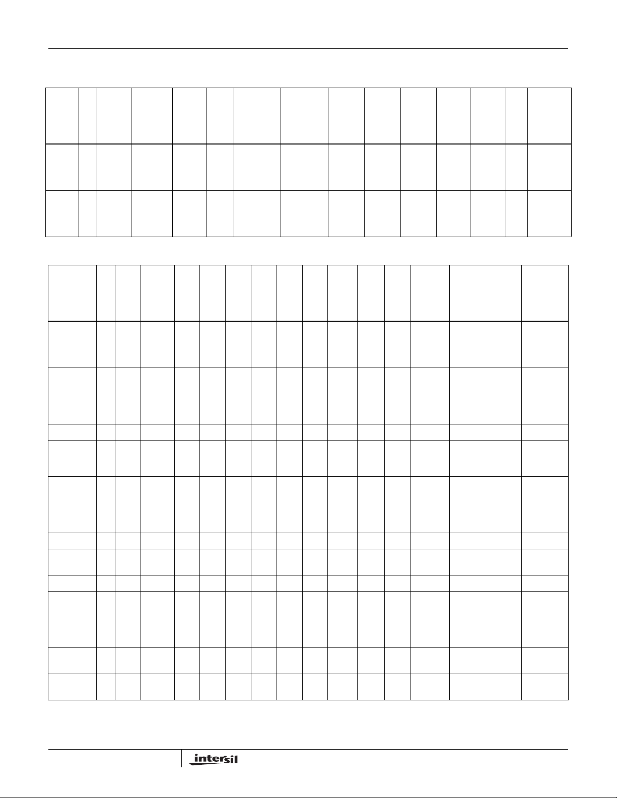
Multiple Cell Li+/Polymer Battery Charger (Continued)
Input Voltage Range: 7V to 25V, Topology: Fixed Freq uency Synchronous Buck, Audible Noise: No, Operating Temperature Range: -10°C to 100°C, Thermal Shutdown: +150°C
Input
Current
Limit
Accuracy
Device iSim
ISL6258A ±3 6.144 to
ISL88731 ±3 2.7 to 19.2
(%)
Battery
Charge
Voltage
19.2 in
16mV Steps
in 16mV
Steps
(V)
Charging
Voltage
Accuracy
(max)
(%)
±0.5 16mV
±0.5 16mV
Battery
Charge
Voltage
Adjust
(%)
Steps
steps
Charge
Current Limit
Accuracy
(%)
±3 128mA to
±3 64mA to
Trickle
Charge
Current Limit
Accuracy
(%)
384mA
220mA
Automatic
Trickle
Charge
(typ)
(V)
Yes
(Threshold
Set by
User)
2.7 2
Battery
Leakage
Current
(max)
(µA)
25
(DCIN=0V,
No System
Load)
(DCIN=0V,
No System
Load)
Automatic
Power
Source
Selection
(Set by
Host)
Adapter
Detection
Yes No 400 99.9 28 Ld TQFN
No
DC
No
(Set by
Host)
Switching
Freq.
(kHz)
Max
Duty
(typ)
Cycle
(%) Package
400 99.9 28 Ld QFN
Single Cell Li+/Polymer Battery Chargers
V
V
IN1
Trickle
V
Voltage
OUT
(typ)
Accuracy
Device iSim
ISL6291 4.1, 4.2 1 13.5 N/A 2 N/A Y Y N 10 N/A Y Enable, Charge Status,
ISL6292 Y 4.1, 4.2 1 7 N/A 1.6
ISL6292B 4.2 1 7 N/A N/A Y Y Y N/A Y 16 Ld QFN
ISL6292C 4.2 1 7 N/A 1.6 N/A Y Y Y 10 N/A Y Enable, Charge Status,
ISL6292D 4.2 1 7 N/A 2.1 N/A Y Y Y 10 N/A Y Enable, Charge Status,
ISL6293 4.2 1 28 5.5 1 0.5 N N N 9.2 8 Y Enable, Charge Status 10 Ld DFN
ISL6294 4.2 1 28 N/A 0.9 N/A N N N 15 N/A Y Enable, Charge Status,
ISL6297 4.2 0.7 7 N/A 1.5 N/A Y Y Y 10 N/A Y Enable 16 Ld QFN
ISL6298 4.1, 4.2 1 7 N/A 0.45 N/A Y Y Y 20 N/A Y Enable, Charge Status,
ISL6299A 4.2 1 28 7 1 0.38 N N N 11 12 Y Enable, Charge Status,
ISL9203R5220 4.2 1 7 N/A 1.6 N/A N N Y 10 N/A Y Enable, Charge Status,
(V)
(%)
V
IN1
(max)
(V)
V
IN2
(max)
(V)
I
I
OUT1
OUT2
(max)
(max)
(A)
(A)
N/A Y Y Y 10 N/A Y Enable, Charge Status,
(DFN)
2.1
(QFN)
Safety
Timer
Self
Term-
ination
Accepts
CC
Adapter
Charge
(min)
(% CC)
IN2
Trickle
Charge
(min)
(% CC)
Thermal
Regulation
Functions
(Pin) Package
Fault Indiction, NTC
Input, Timeout Disable,
Programmable I
Fault Indiction, NTC
Input, Timeout Disable,
Programmable I
Reference Voltage
Fault Indiction,
Reference Voltage
Fault Indiction, NTC
Input, Timeout Disable,
Programmable I
Reference Voltage
Programmable I
Fault Indiction, NTC
Input, Timeout Disable,
Programmable I
Reference Voltage
Programmable I
Reference Voltage
MIN
MIN
MIN
MIN
MIN
MIN
,
,
,
16 Ld QFN
10 Ld DFN,
16 Ld QFN
10 Ld DFN
16 Ld QFN
8 Ld DFN T+R,
8 Ld SOIC
10 Ld DFN,
16 Ld QFN
10 Ld DFN
10 Ld DFN
10-4
1-888-INTERSIL or 1-888-468-3774 | Copyright © 2008 Intersil Americas Inc. All rights reserved.
www.intersil.com
www.intersil.com/power/
www.BDTIC.com/Intersil
Single Cell Li+/Polymer Battery Chargers (Continued)
V
V
IN1
Trickle
V
Voltage
OUT
(typ)
Accuracy
Device iSim
ISL9204 4.2 1 30 N/A 0.35 N/A N N N 19 N/A Y Enable, Charge Status,
ISL9205 4.2 0.6 7 N/A 1 N/A Y Y Y 10 N/A Y Enable, Timout
ISL9205A 4.2 0.6 7 N/A 1 N/A N N Y 10 N/A Y Enable, Charge
ISL9205B 4.2 0.6 7 N/A 1 N/A Y Y Y 10 N/A Y Enable, Charge
ISL9205C 4.256 0.6 7 N/A 1 N/A Y Y Y 10 N/A Y Enable, Charge
ISL9205D 4.2 0.6 7 N/A 1 N/A Y Y Y 10 N/A Y Enable, Charge
ISL9214 4.2 1 28 7 1 0.38 N N N 16 17 Y Enable, Charge Status,
ISL9219 4.2 0.7 28 N/A 1.1 N/A Y Y Y 10 N/A Y Enable, Trickle Mode
ISL9219A 4.2 0.7 28 N/A 1.1 N/A Y Y Y 10 N/A Y Enable, Trickle Mode
ISL9221 4.2 1 28 5.4 1.2 0.465 N Y Y 18 N/A Y Enable, Charge Status,
ISL9222 4.2 1 28 7 1 0.38 N N N 16 17 Y Enable, Programmable
ISL9301 4.5 1 28 N/A 0.8 N/A Y Y Y 6 N/A Y Power Presence,
(V)
(%)
V
IN1
(max)
(V)
V
IN2
(max)
(V)
I
OUT1
(max)
(A)
I
OUT2
(max)
(A)
Safety
Timer
Self
Term-
ination
Accepts
CC
Adapter
Charge
(min)
(% CC)
IN2
Trickle
Charge
(min)
(% CC)
Thermal
Regulation
Functions
(Pin) Package
Power Presence
Indication,
Programmable I
Disable, Charge
Indication, Fault, NTC,
Set, I
I
REF
Set
Indication, Fault, I
Set, I
MIN
Indication, Fault, I
Set, I
MIN
Indication, Fault, I
Set, I
MIN
Indication, Fault, NTC,
I
Set, I
REF
Set
Programmable I
Reference Voltage
Indication, Charge
State Indication,
Adapter Fault, PGOOD,
ISET, NTC Input, Time
Set
Indication, Charge
State Indication,
Adapter Fault, PGOOD,
ISET, NTC Input, Time
Set
Power Present
Indicator
, Power Presence
I
MIN
Indication, Auxiliary
OR-gate For System
Booting Logic
Charge Indication,
Battery Disconnect,
, I
I
REF
Set, Time
MIN
Set, Time Set
Set, Time Set
Set, Time Set
Set, Time
MIN
Set, Time Set
MIN
MIN
MIN
REF
REF
REF
,
8 Ld DFN
16 Ld QFN
10 Ld DFN
10 Ld DFN
10 Ld DFN
10 Ld DFN
10 Ld DFN
20 Ld QFN
20 Ld QFN
12 Ld DFN
8 Ld TDFN
10 Ld DFN
10
Power
Management
10-5
1-888-INTERSIL or 1-888-468-3774 | Copyright © 2008 Intersil Americas Inc. All rights reserved.
www.intersil.com
www.intersil.com/power/
www.BDTIC.com/Intersil
Authentication
Operating
V
Temp. Range
Device
ISL6296 2.6 to 4.8 -25 to +85 110 Single Wire 23 64-Bit Secret with 16x8 OTP ROM 5 Ld SOT-23 T+R,
ISL6296A 2.6 to 4.8 -25 to +85 38 Single Wire 23 64-Bit Secret with 16x8 OTP ROM 5 Ld SOT-23 T+R, 8 Ld TDFN T+R
ISL9206 2.6 to 4.8 -20 to +85 0.15 in Sleep Mode/110 in Run Mode Single Wire 23 FlexiHash+ 5 Ld SOT-23 T+R, 8 Ld DFN T+R
ISL9206A 2.6 to 4.8 -25 to +85 0.15 in Sleep Mode/38 in Run Mode Single Wire 23 FlexiH ash+ 5 Ld SOT-23 T+R, 8 Ld TDFN T+R
(V)
S
(°C)
Supply Current
(µA) Data Bus
Data Bus
Speed
(Kbps) Comments Package
8 Ld DFN T+R
Hot Plug Controllers
Single Channel
Internal FET
V
Device
ISL6121 +2.5 to +5.5 +2.5 to +5.5 Current Regulation (2A) 50 UV Lockout Fault-bar for OC Latch-Off 8 Ld SOIC
BIAS
(V)
External FET
System Management:
System Resets,
Power Indicators,
Device
ISL6115 Y Y Y 12 12 Current
ISL6116 Y Y Y 12 5 Current
ISL6117 Y Y Y 12 3.3 Current
ISL6120 Y Y Y 12 2.5 Current
ISL6140 Y Y N -10 to -80 -10 to -80 Latch-Off Fixed Ext UV/OV
ISL6141 Y Y Y -20 to -80 -20 to -80 Current
ISL6142 Y Y Y -20 to -80 -20 to -80 Current
ISL6150 Y Y N -10 to -80 -10 to -80 Latch-Off Fixed Ext UV/OV
ISL6151 Y Y Y -20 to -80 -20 to -80 Current
ISL6152 Y Y Y -20 to -80 -20 to -80 Current
Fault Detection
Controlled Voltages
(V)
Adjustable
Gate Ramp
Regulation or Latch-Off
for Overcurrent
Advanced Fault
Protection
V
BIAS
(V)
Controlled
Voltages
(V)
r
DS(ON)
(mΩ) UV/OV Feature Reporting Package
Regulation or
Latch-Off for
Overcurrent
Regulation
Regulation
Regulation
Regulation
Regulation
Regulation
Regulation
Regulation
Adjustable
or Fixed
OC Vth
Adjustable UV
Adjustable UV
Adjustable UV
Adjustable UV
Fixed Ext UV/OV
Fixed Ext UV/OV
Fixed Ext UV/OV
Fixed Ext UV/OV
Int/Ext
UV/OV
FET
Feature Reporting Package
Lockout
Lockout
Lockout
Lockout
Lockout
Lockout
Lockout
Lockout
Lockout
Lockout
PGOOD +
Fault Off
PGOOD +
Fault Off
PGOOD +
Fault Off
PGOOD +
Fault Off
PWRGD-bar 8 Ld SOIC
PWRGD-bar 8 Ld SOIC
PWRGD-bar 14 Ld SOIC
PWRGD 8 Ld SOIC
PWRGD 8 Ld SOIC
PWRGD 14 Ld SOIC
8 Ld SOIC
8 Ld SOIC
8 Ld SOIC
8 Ld SOIC
10-6
1-888-INTERSIL or 1-888-468-3774 | Copyright © 2008 Intersil Americas Inc. All rights reserved.
www.intersil.com

www.intersil.com/power/
www.BDTIC.com/Intersil
Dual Channel
Internal FET
V
Device
ISL6119 +2.5 to +5.5 +2.5 to +5.5 Current Regulation (1A) 80 UV Lockout FAULT-bar for OC 8 Ld SOIC
ISL6118 +2.5 to +5.5 +2.5 to +5.5 Current Regulation (0.6A) 80 UV Lockout FAULT-bar for OC 8 Ld SOIC
BIAS
(V)
Controlled Voltages
(V)
Regulation or Latch-Off
for Overcurrent
r
DS(ON)
(mΩ) UV/OV Feature Reporting Package
External FET
Current Regulation or
V
Device
HIP1012A 12 +12 and +5 or +5 and +3.3 Current Regulation Ext UV Notification PGOOD for UV or OC 14 Ld SOIC
HIP1013 12 +12 and +5 or +5 and +3.3 Latch-Off Ext UV Notification PGOOD for UV or OC 14 Ld SOIC
HIP1020 +12 or +5 ≤Bias Voltage N /A Ext N/A N/A 5 Ld SOT-23 T+R
ISL6160 12 +12 and +5 Current Regulation Ext for +12V, Int for +5V UV Lockout FAULT-bar for UV or OC 14 Ld SOIC
ISL6161 12 +12 and +3.3 Current Regulation Ext UV Notification PGOOD for UV or OC 14 Ld SOIC
ISL6173 2.2 to 3.6 0.7 to 3.3 Current Regulation Ext UV PGOOD and FAULT 28 Ld QFN
BIAS
(V)
Controlled Voltages
(V)
Latch-Off
for Overcurrent
Int/Ext
FET UV/OV Feature Reporting Package
PCI
Single Slot
V
Device
HIP1011 12 +12 , -12, +5 , +3.3 Latch-Off Int and Ext UV Lockout UV and OC N 16 Ld SOIC
HIP1011A 12 +12 , -12, +5 , +3.3 Latch-Off Int and Ext UV Lockout UV and OC N 16 Ld SOIC
HIP1011B 12 +12 , -12, +5 , +3.3 Latch-Off Int and Ext UV Lockout OC N 16 Ld SOIC
ISL6111 12 +12 , -12, +5 , +3.3 Current Regulation Int and Ext UV Lockout PGOOD for OC N 20 Ld QFN
BIAS
(V)
Dual Slot
V
Device
HIP1011D 12 +12 , -12, +5 , +3.3 Latch-Off Int and Ext UV Lockout UV and OC N 28 Ld SSOP
HIP1011E 12 +12 , -12, +5 , +3.3 Latch-Off Int and Ext UV Lockout OC N 28 Ld SSOP
BIAS
(V)
Controlled Volt ages
(V)
Controlled Volt ages
(V)
Regulation or Latch-Off
for Overcurrent
Regulation or Latch-Off
for Overcurrent
Int/Ext
FET UV/OV Feature Reporting SM Bus Package
Int/Ext
FET UV/OV Feature Reporting SM Bus Package
10
Power
Management
PCI Express
Dual Slot
V
Device
ISL6112 3.3 +12 and +3.3 and 3.3 Aux Current Regulation Int and Ext UV Lockout PGOOD for UV or OC Y 48 Ld QFN,
ISL6113 3.3 +12 and +3.3 and 3.3 Aux Current Regulation Int and Ext UV Lockout PGOOD for UV or OC,
ISL6114 3.3 +12 and +3.3 and 3.3 Aux Current Regulation Int and Ext UV Lockout PGOOD for UV or OC,
BIAS
(V)
Controlled Volt ages
(V)
10-7
Regulation or Latch-Off
for Overcurrent
Int/Ext
FET UV/OV Feature Reporting SM Bus Package
PE Reset
PE Reset
1-888-INTERSIL or 1-888-468-3774 | Copyright © 2008 Intersil Americas Inc. All rights reserved.
48 Ld TQFP
N 48 Ld QFN
N 48 Ld QFN
www.intersil.com
www.intersil.com/power/
www.BDTIC.com/Intersil
Isolated Power
Single-Ended (Flyback and Forward)
Device iSim Device Description Control Mode
ISL6401 Y Synchronizing Current Mode PWM for
Subscriber Line Interface Circuits
(SLICs)
ISL6721 Y Flexible Single Ended Current Mode
PWM Controller
ISL6722A Flexible Single Ended Current Mode
PWM Controllers
ISL6723A Flexible Single Ended Current Mode
PWM Controllers
ISL6840 Improved Industry-Standard
Single-Ended PWM Controller
ISL6841 Improved Industry-Standard
Single-Ended PWM Controller
ISL6842 Improved Industry-Standard
Single-Ended PWM Controller
ISL6843 Improved Industry-Standard
Single-Ended PWM Controller
ISL6844 Y Improved Industry-Standard
Single-Ended PWM Controller
ISL6845 Improved Industry-Standard
Single-Ended PWM Controller
ISL8840A High Performance Industry Standard
Single-Ended Current Mode PWM
Controller
ISL8841A High Performance Industry Standard
Single-Ended Current Mode PWM
Controller
ISL8842A High Performance Industry Standard
Single-Ended Current Mode PWM
Controller
ISL8843 Single-Ended Current Mode PWM
Controller with 3% Current Limi t an d
Military Temp Grade Option
ISL8843A High Performance Industry Standard
Single-Ended Current Mode PWM
Controller
ISL8844A High Performance Industry Standard
Single-Ended Current Mode PWM
Controller
ISL8845A High Performance Industry Standard
Single-Ended Current Mode PWM
Controller
Peak Current Mode 4.1 3.6 7 3.7 1 1 50 14 Ld SOIC,
Peak Current Mode 8.25 7.7 20 4.5 1 1 100 16 Ld SOIC,
Peak Current Mode 8.25 7.7 20 4.5 1 1 100 16 Ld QFN,
Peak Current Mode 13 7.7 20 4.5 1 1 100 16 Ld SOIC
Peak Current Mode 7 6.6 20 2.3 1 1 100 8 Ld DFN T+R,
Peak Current Mode 7 6.6 20 2.3 1 1 50 8 Ld DFN T+R,
Peak Current Mode 14.4 8.8 20 2.3 1 1 100 8 Ld DFN T+R,
Peak Current Mode 8.4 7.6 20 2.3 1 1 100 8 Ld DFN T+R,
Peak Current Mode 14.4 8.8 20 2.3 1 1 50 8 Ld DFN T+R,
Peak Current Mode 8.4 7.6 20 2.3 1 1 50 8 Ld DFN T+R,
Peak Current Mode 7 6.6 30 2.9 1 1 100 8 Ld MSOP, 8 Ld SOIC
Peak Current Mode 7 6.6 30 2.9 1 1 50 8 Ld MSOP, 8 Ld SOIC
Peak Current Mode 14.4 8.8 30 2.9 1 1 100 8 Ld MSOP, 8 Ld SOIC
Peak Current Mode 8.4 7.6 30 2.9 1 1 100 8 Ld MSOP, 8 Ld SOIC
Peak Current Mode 8.4 7.6 30 2.9 1 1 100 8 Ld MSOP, 8 Ld SOIC
Peak Current Mode 14.4 8.8 30 2.9 1 1 50 8 Ld MSOP, 8 Ld SOIC
Peak Current Mode 8.4 7.6 30 2.9 1 1 50 8 Ld MSOP, 8 Ld SOIC
UVLO
Rising
(V)
UVLO
Falling
(V)
V
BIAS
(max)
(V)
No-Load
Operating
Current
(mA)
# of PWM
Outputs
FET Driver
I
OUT
(max)
(A)
Max Duty
Cycle
(%) Package
16 LdQFN
16 Ld TSSOP
16 Ld SOIC,
16 Ld TSSOP
8 Ld MSOP, 8 Ld SOIC
8LdMSOP, 8Ld SOIC
8LdMSOP, 8Ld SOIC
8LdMSOP, 8Ld SOIC
8LdMSOP, 8Ld SOIC
8LdMSOP, 8Ld SOIC
10-8
1-888-INTERSIL or 1-888-468-3774 | Copyright © 2008 Intersil Americas Inc. All rights reserved.
www.intersil.com
www.intersil.com/power/
www.BDTIC.com/Intersil
Double-Ended (Push-pull, Bridge, Bus Converters, Interleaved)
UVLO
UVLO
Rising
Falling
Device iSim Device Description Control Mode
ISL6740 Y Flexible Double-Ended Voltage-Mode
PWM Controller
ISL6740A Y Flexible Double-Ended Voltage-Mode
PWM Controller with Voltage Feed
Forward
ISL6741 Y Flexible Double-Ended Peak-Current-
Mode PWM Controller
ISL6742 Y Advanced Double-Ended PWM
Controller with Synchronous Rectifier
Control and Average Current Limit
ISL6744 Y Intermediate Bus Double-Ended PWM
Controller with Precision Dead-Time
Adjustment
ISL6744A Intermediate Bus PWM Controller Voltage Mode 6.2 5.7 20 3 2 1 100 8 Ld MSOP, 8 Ld SOIC
ISL6745 Voltage-Mode Double-Ended PWM
Controller with Precision Dead-Time
Adjustment
Voltage Mode 7.25 6.75 20 5 2 0.5 100 16 Ld SOIC,
Voltage Mode 7.25 6.75 20 5 2 0.5 100 16 Ld TSSOP
Peak Current Mode 7.25 6.75 20 5 2 0.5 100 16 Ld SOIC,
Voltage, Peak
Current, or Average
Current Mode
Voltage Mode 6.2 5.7 20 3 2 1 100 8 Ld MSOP, 8 Ld SOIC
Voltage Mode 6.3 5.7 20 3 2 1 100 10 Ld MSOP
(V)
(V)
8.75 7 20 5 4 0.1 100 16 Ld QSOP
V
BIAS
(max)
(V)
No-Load
Operating
Current
(mA)
# of PWM
Outputs
FET Driver
I
OUT
(max)
(A)
Max Duty
Cycle
(%) Package
16 Ld TSSOP
16 Ld TSSOP
Zero-Voltage-Switching (ZVS) Full Bridge
UVLO
UVLO
Rising
Falling
Device iSim Device Description Control Mode
ISL6551 ZVS Full Bridge PWM Controller Peak Current Mode 9.6 8.6 16 13 6 2 100 28 Ld QFN, 28 Ld SOIC
ISL6752 Y ZVS Full-Bridge Current-Mode PWM
with Adjustable Synchronous Rectifier
Control
ISL6753 Y ZVS Full-Bridge PWM Controller Peak Current Mode
Peak Current Mode 8.75 7 20 6 6 0.1 100 16 Ld QSOP
or Voltage Mode
(V)
(V)
8.75 7 20 5 4 0.1 100 16 Ld QSOP
V
BIAS
(max)
(V)
No-Load
Operating
Current
(mA)
# of PWM
Outputs
FET Driver
I
OUT
(max)
(A)
Max Duty
Cycle
(%) Package
LNB Controllers
Single
V
(min)
Device
ISL6421 8 14 13 18 750 1.5 Eval Board, 32 Ld QFN
ISL6421A 8 14 13 18 500 1.5 Eval Board, 32 Ld QFN
ISL6423 8 14 13.3/14.3 18.3/19.3 750 1.5 Eval Board, 24 Ld QFN, 28 Ld HTSSOP
ISL6423B 8 14 13.3/14.3 18.3/19.3 750 1.5 24 Ld QFN, 28 Ld EPTSSOP
ISL6425 8 14 13 18 750 1.5 Eval Board, 32 Ld QFN
IN
(V)
VIN (max)
(V)
V
OUT
(min)
(V)
V
OUT
(max)
(V)
I
OUT
(max)
(mA)
I
(min)
BIAS
(mA) Package
10
Power
Management
10-9
1-888-INTERSIL or 1-888-468-3774 | Copyright © 2008 Intersil Americas Inc. All rights reserved.
www.intersil.com
www.intersil.com/power/
www.BDTIC.com/Intersil
Dual
(min)
V
IN
Device
ISL6405 8 14 13 18 750 1.5 Eval Board, 32 Ld QFN
ISL6422 8 14 2x13.3/14.3 2x18.3/19.3 2x750 3 38 Ld EPTSSOP, 40 Ld QFN
ISL6422B 8 14 2x13.3/14.3 2x18.3/19.3 2x750 3 38 Ld EPTSSOP, 40 Ld QFN
ISL6424 8 14 13 18 750 1.5 Eval Board, 32 Ld QFN
(V)
VIN (max)
(V)
V
OUT
(min)
(V)
V
OUT
(max)
(V)
I
OUT
(max)
(mA)
I
(min)
BIAS
(mA) Package
Linear Regulation
Low Noise
V
IN
(min)
Device
ICL7663S 1.6 16 1.3 16 40 8 Ld PDIP, 8 Ld SOIC
ISL6412 3 3.6 1.8 2.8 840 16 Ld QFN
ISL6414 3 3.6 1.8 2.84 500 16 Ld QFN
ISL6416 3 3.6 1.8 2.8 500 16 Ld QSOP
(V)
V
IN
(max)
(V)
V
OUT
(min)
(V)
V
OUT
(max)
(V)
I
OUT
(max)
(mA) Package
Low Power
V
IN
Range
Device iSim
ISL9000 Y 2.3 to
ISL9000A 2.3 to
ISL9001 2.3 to
ISL9001A 2.3 to
ISL9003A 2.3 to
ISL9005 2.3 to
ISL9005A 2.3 to
ISL9007 2.3 to
ISL9008A 2.3 to
ISL9011 2.3 to
ISL9011A 2.3 to
ISL9012 2.3 to
(V)
6.5
6.5
6.5
6.5
6.5
6.5
6.5
6.5
6.5
6.5
6.5
6.5
V
OUT
Range
(V)
1.5 to
3.3
1.5 to
3.3
1.5 to
3.3
1.5 to
3.3
1.5 to
3.3
1.5 to
3.3
1.5 to
3.3
1.5 to
3.3
1.5 to
3.3
1.5 to
3.3
1.5 to
3.3
1.5 to
3.3
Fixed
Output
O/P Volt
Voltage
Accuracy
Option
(%)
Y ±1.8 300 300 90 30 40 250 @
Y ±1.8 300 300 90 30 40 250 @
Y ±1.8 300 90 30 25 250 @
Y ±1.8 300 90 30 25 250 @
Y ±1.8 150 N/A 90 20 29 200
Y ±1.8 300 75 45 50 250 @
Y ±1.8 300 75 45 50 250 @
Y ±1.8 400 75 30 50 250 @
Y ±1.8 150 N/A 65 45 45 200
Y ±1.8 150 300 70 30 45 250 @
Y ±1.8 150 300 70 30 45 250 @
Y ±1.8 150 300 70 30 45 250 @
I
OUT1
(max)
(mA)
I
OUT2
(max)
(mA)
PSRR
@ 1kHz
(dB)
(V
Noise
10 to 100)
RMS
(kHz)
Iq
(µA)
Typical
Drop-Out
Voltage
(mV)
300mA
300mA
300mA
300mA
@150mA
300mA
300mA
400mA
@150mA
300mA
300mA
300mA
Operating
Enable/
Shutdown
# of
Temp. Range
PORs
Y 2 -40 to +85 Eval Board,
Y 2 -40 to +85 10 Ld DFN
Y -40 to +85 8 Ld DFN T+R
Y -40 to +85 8 Ld DFN T+R
Y N/A -40 to +85 5 Ld SC-70 T+R,
Y -40 to +85 8 Ld DFN T+R
Y -40 to +85 8 Ld DFN T+R
Y -40 to +85 8 Ld MSOP
Y N/A -40 to +85 5 Ld SC-70 T+R,
Y -40 to +85 10 Ld DFN
Y -40 to +85 10 Ld DFN
Y 1 -40 to +85 10 Ld DFN
(°C) Package
10 Ld DFN
6 Ld µTDFN T+R
6 Ld µTDFN T+R
10-10
1-888-INTERSIL or 1-888-468-3774 | Copyright © 2008 Intersil Americas Inc. All rights reserved.
www.intersil.com
www.intersil.com/power/
www.BDTIC.com/Intersil
Low Power (Continued)
V
IN
Device iSim
ISL9014 2.3 to
ISL9014A 2.3 to
Range
(V)
6.5
6.5
V
OUT
Range
(V)
1.5 to
3.3
1.5 to
3.3
Fixed
I
Output
O/P Volt
Voltage
Accuracy
Option
Y ±1.8 300 300 70 30 45 250 @
Y ±1.8 300 300 70 30 45 250 @
(%)
I
OUT1
(max)
(mA)
OUT2
(max)
(mA)
PSRR
@ 1kHz
(dB)
(V
Noise
10 to 100)
RMS
(kHz)
Iq
(µA)
Typical
Drop-Out
Voltage
(mV)
300mA
300mA
Operating
Enable/
Shutdown
# of
Temp. Range
PORs
Y -40 to +85 10 Ld DFN
Y -40 to +85 10 Ld DFN
High Voltage
V
IN
(min)
Device iSim
ISL6720A Y 17 100 0 20 125 1.2 11 Ld DFN
ISL6719 17 100 1.5 20 100 1.1 9 Ld DFN
(V)
V
IN
(max)
(V)
V
OUT
(min)
(V)
V
OUT
(max)
(V)
I
OUT
(max)
(mA)
I
BIAS
(min)
(mA) Package
Power MOSFET Drivers
Integrated FET Bridge and High-Side Drivers
Device Device Description
HIP4020 Full Bridge Driver with Integrated
0.5A Power FETs for Small 3V, 5V
and 12V DC Motors
ISL6801 High Voltage Bootstrap High Side
Driver
Max Bootstrap
Supply Voltage
(V)
N/A 15 0.5 0.5 2.5 0.1 4 0.1 20 Ld SOIC
120 6.5 0.2 0.2 1 0.1 4 0.1 8 Ld SOIC
Max Bias
Voltage
(V)
Sourcing Current
Capability
(A)
Sinking Current
Capability
(A)
Turn-On
Prop Delay
(µs)
Turn-Off
Prop Delay
(µs)
Rise
Time
(µs)
(°C) Package
Fall
Time
(µs) Package
10
Full Bridge and Three-Phase
Max Bootstrap
Supply Voltage
Device Device Description
HIP4080A 80V/2.5A Peak, High Frequency Full
Bridge FET Driver with Charge Pump
and Input Comparators
HIP4081A 80V/2.5A Peak, High Frequency Full
Bridge FET Driver with Charge Pump
and Independent Control Inputs
HIP4082 80V/1.25A Peak Current Full Bridge
FET Driver
HIP4083 80V/0.3A Peak Three Phase High Side
Driver
HIP4086 80V/0.5A Peak Three Phase Driver 95 15 0.5 1.1 65 75 20 10 24 Ld PDIP,
ISL83202 55V, 1A Peak Current H-Bridge FET
Driver
ISL83204A 60V/2.5A Peak, High Frequency Full
Bridge FET Driver
(V)
95 15 2.6 2.4 70 50 10 10 20 Ld PDIP,
95 15 2.6 2.4 60 35 10 10 20 Ld PDIP,
95 15 1.4 1.3 75 55 9 9 16 Ld PDIP,
95 15 0.24 (avg) 0.3 (avg) 65 60 35 30 16 Ld PDIP,
70 15 1 1 75 55 9 9 16 Ld PDIP,
75 15 2.6 2.4 70 50 10 10 20 Ld PDIP,
Max Bias
Voltage
(V)
Peak Pull-up
Current
(A)
Peak Pull-down
Current
(A)
Turn-On
Prop Delay
(ns)
Turn-Off
Prop Delay
(ns)
Rise
Fall
Time
Time
(ns)
(ns) Package
20 Ld SOI C
20 Ld SOI C
16 Ld SOI C
16 Ld SOI C
24 Ld SOI C
16 Ld SOI C
20 Ld SOI C
Power
Management
10-11
1-888-INTERSIL or 1-888-468-3774 | Copyright © 2008 Intersil Americas Inc. All rights reserved.
www.intersil.com
Half Bridge
www.BDTIC.com/Intersil
Device Device Description
HIP2100 100V/2A Peak High-Frequency Half
Bridge Driver with CMOS Logic Inputs
HIP2101 100V/2A Peak High-Frequency Half
Bridge Driver with TTL Logic Inputs
ISL2100A 100V, 2A Peak, High Frequency Half-
Bridge Drivers
ISL2101A 100V, 2A Peak, High Frequency Half-
Bridge Drivers
ISL2110 100V, 3A/4A Peak, High Frequency
Half-Bridge Drivers
ISL2111 100V, 3A/4A Peak, High Frequency
Half-Bridge Drivers
ISL6700 80V/1.25A Peak High-Frequency Half
Bridge Driver with TTL Logic Inputs
ISL89400 100V, 1.25A Peak, High Frequency
Half-Bridge Drivers
ISL89401 100V, 1.25A Peak, High Frequency
Half-Bridge Drivers
www.intersil.com/power/
Max Bootstrap
Supply Voltage
(V)
114 14 2 2 20 20 10 10 12 Ld DFN,
114 14 2 2 25 25 10 10 12 Ld DFN,
114 14 2 2 39 31 10 10 9 Ld DFN
114 14 2 2 39 34 10 10 9 Ld DFN
114 14 3 4 3 8 32 9 7.5 12 Ld DFN,
114 14 3 4 38 32 9 7.5 10 Ld TDFN,
96 15 1.4 1.3 70 60 5 5 12 Ld QFN,
114 14 1.25 1.25 39 31 16 16 9 Ld DFN,
114 14 1.25 1.25 39 31 16 16 9 Ld DFN,
Max Bias
Voltage
(V)
Peak Pull-up
Current
(A)
Peak Pull-down
Current
(A)
Turn-On
Prop Delay
(ns)
Turn-Off
Prop Delay
(ns)
Rise
Fall
Time
Time
(ns)
(ns) Package
16 Ld QFN,
8 Ld EPSOIC,
8 Ld SOIC
16 Ld QFN,
8 Ld EPSOIC,
8 Ld SOIC
8LdSOIC
12 Ld DFN,
8LdSOIC
8LdSOIC
8LdSOIC
8LdSOIC
Low Side
Single
Device
Device
EL7104 High Speed, Single
EL7154 High Speed,
EL7155 High Performance
EL7156 High Performance
EL7158 Ultra-High Current
EL7182 2-Phase, High Speed
Description
Channel, Power
MOSFET Driver
Monolithic Pin Driver
Pin Driver
Pin Driver
Pin Driver
CCD Driver
Max
Operating
# of
Frequency
Drivers
(MHz)
1 10 4 10 15 18 18 7.5 1.5 0 to
1 10 4 20 20 10 20 2.5 1.5 0 to
1 40 3.5 14.5 15 10 9.5 3 2.7 0 to
1 40 3.5 14.5 15 10 9.5 3 2.7 0 to
1 40 12 12 12 22 22.5 2.5 0.5 0 to
2 10 2 10 13 18 20 5 3 +4.5 to
Peak
Output
I
PK
(A)
Rise
Time
(ns)
Fall
Time
(ns)
Turn On
Delay
(ns
Turn Off
Delay
(ns)
I
S
(mA)
R
(Ω)
Input
Signal
Range
ON
(V)
V
P
V
P
V
P
V
P
V
P
Input
Supply
Range
(VP)
+4.5 to
+16
+4.5 to
+16
+4.5 to
+16.5
+4.5 to
+16.5
+4.5 to
+18
+16
Max
Max
Output
Input
Signal
Signal
Range
(V)
16 8 Ld PDIP,
16 -3 to +15.5 15.5 8 Ld PDIP,
16 -5 to +16.5 16 8 Ld PDIP,
16 -5 to +16.5 16 8 Ld PDIP,
18 -5 to +12 12 8 Ld SOIC
16 8 Ld PDIP,
(V)
Output
Signal
Range
(V) Package
8 Ld SOIC
8 Ld SOIC
8 Ld SOIC
8 Ld SOIC
8 Ld SOIC
10-12
1-888-INTERSIL or 1-888-468-3774 | Copyright © 2008 Intersil Americas Inc. All rights reserved.
www.intersil.com
www.intersil.com/power/
www.BDTIC.com/Intersil
Dual
V
Max Operating
IN
(max)
Device Device Description
EL7202 High Speed, Dual Channel Power MOSFET
Drivers
EL7212 High Speed, Dual Channel Power MOSFET
Drivers
EL7222 High Speed, Dual Channel Power MOSFET
Drivers
EL7232 Dual Channel, High Speed, High Current Line
Driver with 3-State
EL7242 Dual Input, High Speed, Dual Channel Power
MOSFET Driver
EL7252 Dual Input, High Speed, Dual Channel Power
MOSFET Driver
ICL7667 Dual Power MOSFET Driver 15 10 1 30 30 20 5 4.5 8 Ld PDIP,
Frequency
(V)
15 10 2 10 13 1 8 20 7.5 4.5 8 Ld PDIP,
15 10 2 10 13 1 8 20 2.5 4.5 8 Ld PDIP,
15 10 2 10 13 18 20 5 4.5 8 Ld PDIP,
15 10 2 10 13 1 8 20 2.5 4.5 8 Ld PDIP,
15 10 2 20 (max) 2 0 (m a x) 20 20 3 4.5 8 Ld P D IP,
15 10 2 20 (max) 20 (m a x ) 20 3 4.5 8 Ld PDIP,
(MHz)
Peak
Output I
(A)
PK
Rise Time
(ns)
Fall Time
(ns)
Turn On
Delay
(ns)
Turn Off
Delay
(ns)
I
S
(mA)
V
BIAS
(min)
(V) Package
8Ld SOIC
8Ld SOIC
8Ld SOIC
8Ld SOIC
8Ld SOIC
8Ld SOIC
8Ld SOIC
Quad
Signal
Range
(V)
+16
Max
Output
Signal
Range
(V) Package
16 16 Ld QFN,
16 Ld QSOP,
16 Ld SOIC
Device Device Description
EL7412 High Speed, Four
Channel Power
MOSFET Drivers
EL7457 40MHz Non-Inverting
Quad CMOS Driver
Max
Rise
Fall
Operating
# of
Frequency
Drivers
(MHz)
4 10 2 10 13 18 18 5 3 20 Ld SOIC
4 40 2 11 12 13 11.5 0.8 4.5 -V
Peak Output
I
PK
(A)
Time
(ns)
Turn On
Time
(ns)
Delay
(ns)
Turn Off
Delay
(ns)
I
S
(mA)
R
(Ω)
ON
Input
Signal
Range
(V)
to
P
+ V
P
Input
Supply
Range
(VP)
-4.5 to
+16
Max
Input
Signal
(V)
16 -4.5 to
Output
Synchronous Buck
UGATE
Output Per
Driver I
LGATE
Source/Sink
(A)
Phase V
(min)
(V)
GND - 8V
(<400ns)
GND - 8V
(<400ns)
GND - 8V
(<400ns)
GND - 8V
(<400ns)
GND - 8V
(<400ns)
PHASE
Phase V
PHASE
(max)
(V)
15VDC, 30V
(<200ns)
15VDC, 30V
(<200ns)
15VDC, 30V
(<200ns)
15VDC, 30V
(<200ns)
15VDC, 30V
(<200ns)
No Load
IS (max)
(mA)
4.5 7.1 14 Ld SOIC,
4.5 7.1 14 Ld SOIC,
4.5 7.1 14 Ld SOIC,
N/A 4.5 10 Ld DFN,
2.5 8 10 Ld DFN,
I
S
(mA) Package
16 Ld QFN
16 Ld QFN
16 Ld QFN
8 Ld SOIC
8 Ld SOIC
Device Device Descrip tio n
ISL6614 Dual Advanced Synchronous
Rectified Buck MOSFET Drivers
with Protection Features
ISL6614A Dual Advanced Synchronous
Rectified Buck MOSFET Drivers
with Pre-POR OVP
ISL6614B Dual Advanced Synchronous
Rectified Buck MOSFET Drivers
with Protection Features
ISL6594D Advanced Synchronous Buck
MOSFET Driver with 3V PWM
Interface and Advanced
Protection Features
ISL6594A Advanced Synchronous Buck
MOSFET Driver with 3V PWM
Interface and Advanced
Protection Features
Output Per
Driver I
(max)/V
V
IN
(V)
GND - 0.3V to 7V 5 to 12 1.25/2 2/3 GND - 0.3VDC
GND - 0.3V to 7V 5 to 12 1.25/2 2/3 GND - 0.3VDC
GND - 0.3V to 7V 5 to 12 1.25/2 2/3 GND - 0.3VDC
GND - 0.3 V to 7V 4.5 to 13.2 1.25/2 2/3 GND - 0.3VDC
GND - 0.3V to 7V 5 to 12 1.25/2 2/3 GND - 0.3VDC
PWM
V
DRIVE
(V)
Source/Sink
(A)
10
Power
Management
10-13
1-888-INTERSIL or 1-888-468-3774 | Copyright © 2008 Intersil Americas Inc. All rights reserved.
www.intersil.com

Synchronous Buck (Continued)
www.BDTIC.com/Intersil
V
(max)/V
Device Device Descrip tio n
ISL6594B Advanced Synchronous Buck
MOSFET Driver with 3V PWM
Interface and Advanced
Protection Features
ISL6596 Synchronous Rectified MOSFET
ISL6609 Synchronous Rectified MOSFET
ISL6609A Synchronous Rectified MOSFET
ISL6610 Dual Synchronous Rectified
ISL6610A Dual Synchronous Rectified
ISL6612A Advanced Synchronous
ISL6612B Advanced Synchronous
ISL6613A Advanced Synchronous
ISL6613B Advanced Synchronous
ISL6208A High Voltage Synchronous
ISL6605 Synchronous Rectified MOSFET
ISL6608 Synchronous Rectified MOSFET
ISL6207 High Voltage Synchronous
ISL6208 High Voltage Synchronous
ISL6209 High Voltage Synchronous
ISL6210 Dual Synchronous Rectified
HIP6601B Synchronous Rectified Buck
HIP6602B Dual Channel Synchronous
Driver
Driver
Driver
MOSFET Drivers
MOSFET Drivers
Rectified Buck MOSFET Drivers
with Pre-POR OVP
Rectified Buck MOSFET Drivers
with Pre-POR OVP
Rectified Buck MOSFET Drivers
with Pre-POR OVP
Rectified Buck MOSFET Drivers
with Pre-POR OVP
ctified Buck MOSFET Driver
Re
with Programmable Deadtime
Driver
Driver
Rectified Buck MOSFET Driver
Rectified Buck MOSFET Driver
with Programmable Deadtime
Rectified Buck MOSFET Driver
with Programmable Deadtime
MOSFET Drivers
MOSFET Drivers
Rectified Buck MOSFET Driver
IN
GND - 0.3V to 7V 5 to 12 1.25/2 2/3 GND - 0.3VDC
3.3 and 5 5 2/2 2/4 GND - 0.3VDC
-0.3V to VCC
-0.3V to VCC
GND - 0.3V to 7V 5 to 12 1.25/2 2/3 GND - 0.3VDC
GND - 0.3V to 7V 5 to 12 1.25 2 2/3 GND - 0.3VDC
GND - 0.3V to 7V 5 to 12 1.25/2 2/3 GND - 0.3VDC
GND - 0.3V to 7V 5 to 12 1.25/2 2/3 GND - 0.3VDC
-0.3V to VCC
-0.3V to 7V 5 2/2 2/4 V
-0.3V to VCC
-0.3V to VCC
-0.3V to VCC
www.intersil.com/power/
UGATE
Output Per
Driver I
LGATE
Source/Sink
(A)
Phase V
(min)
(V)
GND - 8V
(<400ns)
GND - 8V
(<20ns)
GND - 8V
(<20ns)
GND - 8V
(<400ns)
GND - 8V
(<400ns)
GND - 8V
(<400ns)
GND - 8V
(<400ns)
BOOT
BOOT
BOOT
BOOT
BOOT
BOOT
BOOT
Phase V
PHASE
-7 30 0.08 8 Ld QFN,
-7 22 0.002 8 Ld QFN,
-7 22 0.08 8 Ld QFN,
-7 30 0.05 8 Ld QFN,
-7 30 0.08 8 Ld QFN,
-7 30 0.085 8 Ld QFN,
-7 25 0.17 16 Ld QFN
(max)
(V)
15VDC, 30V
(<200ns)
15VDC, 30V
(<100ns)
(<100ns)
15VDC, 30V
(<100ns)
15VDC, 30V
(<200ns)
15VDC, 30V
(<200ns)
15VDC, 30V
(<200ns)
15VDC, 30V
(<200ns)
PHASE
No Load
IS (max)
(mA)
2.5 4.5 10 Ld DFN,
Almost
Negligible
Almost
Negligible
Almost
Negligible
7.2 5 10 Ld DFN,
4.5 8 10 Ld DFN,
4.5 4.5 10 Ld DFN,
4.5 4.5 10 Ld DFN,
I
S
(mA) Package
8 Ld SOIC
0.19 10 Ld QFN,
8 Ld SOIC
0.132 8 Ld QFN,
8 Ld SOIC
0.132 8 Ld QFN,
8 Ld SOIC
14 Ld SOIC,
(typ)
16 Ld QFN
14 Ld SOIC,
(typ)
16 Ld QFN
8 Ld EPSOIC,
8 Ld SOIC
8 Ld EPSOIC,
8 Ld SOIC
8 Ld EPSOIC,
8 Ld SOIC
8 Ld EPSOIC,
8 Ld SOIC
8 Ld SOIC
8 Ld SOIC
8 Ld SOIC
8 Ld SOIC
8 Ld SOIC
8 Ld SOIC
8 Ld SOIC
16 Ld QFN
Output Per
Driver I
V
PWM
(V)
+0.3V
+0.3V
22 5 2/2 2/4 -8 30 1.6 (typ) 240µA
15 5 2/2 2/4 -8 30 1.6 (typ) 240µA
+0.3V
17 5 2/2 2/4 V
+0.3V
+0.3V
+0.3V
25 5 2 2/4 V
12 5 or 12 0.7 -5 15 6.6 8 Ld EPSOIC,
12 5 or 12 0.7 -5 15 9 14 Ld SOIC,
Source/Sink
DRIVE
(V)
5 2/2 2/4 -8V (<20ns) 15VDC, 30V
5 2/2 2/4 GND - 0.3VDC
52/22/4V
52/22/4V
52/22/4V
52/22/4V
(A)
10-14
1-888-INTERSIL or 1-888-468-3774 | Copyright © 2008 Intersil Americas Inc. All rights reserved.
www.intersil.com
Synchronous Buck (Continued)
www.BDTIC.com/Intersil
V
(max)/V
Device Device Descrip tio n
HIP6603B Synchronous Rectified Buck
MOSFET Drivers
HIP6604B Synchronous Rectified Buck
MOSFET Drivers
PX3511A Advanced Synchronous
Rectified Buck MOSFET Drivers
with Protection Features
PX3511B Advanced Synchronous
Rectified Buck MOSFET Drivers
with Protection Features
PX3511D Advanced Synchronous
Rectified Buck MOSFET Driver
with Protection Features
ISL6622 VR11.1 Compatible
Synchronous Rectified Buck
MOSFET Drivers
ISL6622A VR11.1 Compatible
Synchronous Rectified Buck
MOSFET Drivers
ISL6615 High-Frequency 6A Sink
Synchronous MOSFET Drivers
with Protection Features
ISL6615A High-Frequency 6A Sink
Synchronous MOSFET Drivers
with Protection Features
ISL6620 VR11.1 Compatible
Synchronous Rectified Buck
MOSFET Drivers
ISL6620A VR11.1 Compatible
Synchronous Rectified Buck
MOSFET Drivers
IN
www.intersil.com/power/
UGATE
Output Per
Driver I
LGATE
Source/Sink
(A)
Phase V
(min)
(V)
GND - 8V
(<400ns)
GND - 8V
(<400ns)
GND - 8V
(<400ns)
GND - 8V
(<200ns)
GND - 8V
(<200ns)
GND - 8V
(<400ns)
GND - 8V
(<400ns)
GND - 8V
(<100ns)
GND - 8V
(<100ns)
PHASE
Phase V
PHASE
(max)
(V)
15VDC, 30V
(<200ns)
15VDC, 30V
(<200ns)
15VDC, 30V
(<200ns)
15VDC, 30V
(<200ns)
15VDC, 30V
(<200ns)
15VDC, 30V
(<200ns)
15VDC, 30V
(<200ns)
15VDC, 30V
(<100ns)
15VDC, 30V
(<100ns)
No Load
IS (max)
(mA)
2.5 4.5 10 Ld DFN,
2.5 4.5 10 Ld DFN,
N/A 12 10 Ld DFN T+R
N/A 5.7 10 Ld DFN,
N/A 5.7 10 Ld DFN,
4.5 8 10 Ld DFN,
4.5 8 10 Ld DFN,
1.27 (typ) 1.85
27 (typ) 1.85
1.
I
S
(mA) Package
8 Ld SOIC
8 Ld SOIC
8 Ld SOIC
8 Ld SOIC
8 Ld SOIC
8 Ld SOIC
8 Ld SOIC
10 Ld DFN,
(typ)
8 Ld SOIC
10 Ld DFN,
(typ)
8 Ld SOIC
Output Per
Driver I
DRIVE
(V)
Source/Sink
(A)
V
PWM
(V)
12 5 or 12 0.7 -5 15 7 8 Ld EPSOIC,
12 5 or 12 0.7 -5 15 9.8 16 Ld QFN
15 5 or 12 1.25/2 2/3 GND - 0.3VDC
15 5 or 12 1.25/2 2/3 GND - 0.3VDC
13.2 12 1.25/2 2/3 GND - 0.3VDC
15 5 to 12 1.25/2 2/3 GND - 0.3VDC
15 5 to 12 1.25/2 2/3 GND - 0.3VDC
15 4.5 to 13.2 2.5/4 4/6 GND - 0.3VDC
15 4.5 to 13.2 2.5/4 4/6 GND - 0.3VDC
15 5 2/2 2/4 GND - 0.3VDC
15 5 2/2 2/4 GND - 0.3VDC
10
Power
Management
Power Supply Support
ORing FET Control
V
Device
ISL6144 +10 to +75 100 <300 <100 Voltage Resistor-Adjustable
BIAS
(V)
Transient Voltage
Withstanding
(V)
10-15
Response Time to
Dead Short
(ns)
Response Time to PS
Slow Turn Off
(µs) Ramp
1-888-INTERSIL or 1-888-468-3774 | Copyright © 2008 Intersil Americas Inc. All rights reserved.
Reverse Current
Threshold Package
(0V to 5.3V)
16 Ld TSSOP, 20 Ld QFN
www.intersil.com
www.intersil.com/power/
www.BDTIC.com/Intersil
Power Sequencers
V
Device
HIP1020 +12 or +5 ≤Bias Voltage N/A Ext N/A N/A 5 Ld SOT-23 T+R
Device
ISL6123 +1.5 to +5.5 +0.7 to +5.5 Up to 4 Active High Charge Pumped FET Drive UV Latch-Off 24 Ld QFN
ISL6124 +1.5 to +5.5 +0.7 to +5.5 Up to 4 Active Low Charge Pumped FET Drive UV Latch-Off 24 Ld QFN
ISL6125 +1.5 to +5.5 >+0.7 Up to 4 Active Low Open Drain Logic UV Latch-Off 24 Ld QFN
ISL6126 +1.5 to +5.5 +0.7 to +5.5 Up to 4 Active Low Charge Pumped FET Drive UV Latch-Off 24 Ld QFN
ISL6127 +1.5 to +5.5 +0.7 to +5.5 Up to 4 Active Low Charge Pumped FET Drive UV Latch-Off 24 Ld QFN
ISL6128 +1.5 to +5.5 +0.7 to +5.5 Up to 4 Active Low Charge Pumped FET Drive UV Latch-Off 24 Ld QFN
ISL6130 +1.5 to +5.5 +0.7 to +5.5 Up to 4 Active High Charge Pumped FET Drive UV Latch-Off 24 Ld QFN
BIAS
(V)
V
Range
BIAS
(V)
Controlled Voltages
(V)
Sequenced Voltages or Range
(V)
Regulation or Latch-Off for
Overcurrent Int/Ext FET UV/OV Feature Reporting Package
# of Voltages
Sequenced Enable Output UV/OV Feature Package
V
Device
ISL8700 2.5 to 24 Auto 4 Active High, Open Drain N N/A 14 Ld SOIC
ISL8700A 3.3 to 24 Auto 4 Active High, Open Drain N N/A 14 Ld SOIC
ISL8701 2.5 to 24 Auto 4 Active Low, Open Drain N N/A 14 Ld SOIC
ISL8701A 3.3 to 24 Auto 4 Active Low, Open Drain N N/A 14 Ld SOIC
ISL8702 2.5 to 12 Active High 4 Active High, Open Drain Y Power Fault 14 Ld SOIC
ISL8702A 3.3 to 24 SEQ_ENABLE 4 Active High, Open Drain Y UV/OV 14 Ld SOIC
ISL8703A 3.3 to 24 SEQ_ENABLE 4 Active Low, Open Drain Y UV/OV 14 Ld SOIC
ISL8704A 3.3 to 24 SEQ_ENABLE# 4 Act ive High, Open Drain Y UV/OV 14 Ld SOIC
ISL8705A 3.3 to 24 SEQ_ENABLE# 4 Active Low, Open Drain Y UV/OV 14 Ld SOIC
ISL8723 2.5 to 5 SEQ_ENABLE 4 Charge Pumped FET Drive Y UV Latch-Off 24 Ld QFN
ISL8724 2.5 to 5 SEQ_ENABLE# 4 Charge Pumped FET Drive Y UV Latch-Off 24 Ld QFN
BIAS
(V) SEQ_ENABLE
# of Sequenced
ENABLE Outputs
ENABLE
Output Type
Power Down
Sequencing
Conditions
Reported Package
Supervisors
Voltage Monitors with EEPROM I2C Interface
Single
Range (V)
Device
X4003 4.5 to 5.5
X4005 4.5 to 5.5
S
V
4.5 to 5.5
2.7-5.5)
2.7 to 5.5
4.5 to 5.5
2.7 to 5.5
2.7 to 5.5
Voltage Thresh old 1
4.62 (2.6%)
4.38 (3%)
2.92 (2.4%)
2.62 (2.7%)
4.62 (2.6%)
4.38 (3%)
2.92 (2.4%)
2.62 (2.7%)
Reset Output Type
Active High OFF, 0.6, 0.2, 1.4 N I
Active Low OFF, 0.6, 0.2, 1.4 N I
Watchdog Timer (s)
Manual Reset
Bus Interface
EEPROM Size (kbits)
Battery Montor and Switchover
Fault Detection Register
Suffix
2
C0 N N-4.5A
2
C0 N N-4.5A
Blank
-2.7A
-2.7
Blank
-2.7A
-2.7
10-16
1-888-INTERSIL or 1-888-468-3774 | Copyright © 2008 Intersil Americas Inc. All rights reserved.
POR (ms)
RTC Function
Features
200 N 8 Ld MSOP,
200 N 8 Ld MSOP,
www.intersil.com
Package
8 Ld SOIC
8 Ld SOIC
www.intersil.com/power/
www.BDTIC.com/Intersil
Single (Continued)
Range (V)
Device
X4043 4.5 to 5.5
X4045 4.5 to 5.5
X4C105 3.0 to 3.6 2.875 (2.6%) Active High N N I
Dual
S
V
4.5 to 5.5
2.7 to 5.5
2.7 to 5.5
4.5 to 5.5
2.7 to 5.5
2.7 to 5.5
Voltage Threshold 1
4.62 (2.6%)
4.38 (3%)
2.92 (2.4%)
2.62 (2.7%)
4.62 (2.6%)
4.38 (3%)
2.92 (2.4%)
2.62 (2.7%)
Reset Output Type
Active High OFF, 0.6, 0.2, 1.4 N I
Active Low OFF, 0.6, 0.2, 1.4 N I
Watchdog Timer (s)
Manual Reset
Bus Interface
EEPROM Size (kbits)
Battery Montor and Switchover
Fault Detection Register
Suffix
POR (ms)
RTC Function
Features
2
C4 N N-4.5A
2
C4 N N-4.5A
2
C 4 N N None 200 N NOVRAM 20 Ld TSSOP
Blank
Blank
200 N 8 Ld MSOP,
-2.7A
-2.7
200 N 8 Ld MSOP,
-2.7A
-2.7
Package
8 Ld PDIP,
8LdSOIC
8 Ld PDIP,
8LdSOIC
Range (V)
Device
X40010 2.7 to 5.5
X40011 2.7 to 5.5
X40014 2.7 to 5.5
X40015 2.7 to 5.5
X40020 2.7 to 5.5
X40021 2.7 to 5.5
X40410 2.7 to 5.5
X40411 2.7 to 5.5
X40414 2.7 to 5.5
S
V
2.7 to 5.5
2.7 to 3.6
2.7 to 5.5
2.7 to 3.6
2.7 to 5.5
2.7 to 3.6
2.7 to 5.5
2.7 to 3.6
2.7 to 5.5
2.7 to 3.6
2.7 to 5.5
2.7 to 3.6
2.7 to 5.5
2.7 to 3.6
2.7 to 5.5
2.7 to 3.6
2.7 to 5.5
2.7 to 3.6
Voltage Threshold 1
4.6 (1%)
4.6 (1%)
2.9 (1.7%)
4.6 (1%)
4.6 (1%)
2.9 (1.7%)
2.9 (1.7%)
2.6 (2%)
2.6 (2%)
2.9 (1.7%)
2.6 (2%)
2.6 (2%)
4.6 (1%)
4.6 (1%)
2.9 (1.7%)
4.6 (1%)
4.6 (1%)
2.9 (1.7%)
4.6 (1%)
4.6 (1%)
2.9 (1.7%)
4.6 (1%)
4.6 (1%)
2.9 (1.7%)
2.9 (1.7%)
2.6 (2%)
2.6 (2%)
Voltage Threshold 2
2.9 (1.7%)
2.6 (2%)
1.6 (3%)
2.9 (1.7%)
2.6 (2%)
1.6 (3%)
1.3 (4%)
1.3 (4%)
1.0 (5%)
1.3 (4%)
1.3 (4%)
1.0 (5%)
2.9 (1.7%)
2.6 (2%)
1.6 (3%)
2.9 (1.7%)
2.6 (2%)
1.6 (3%)
2.9 (1.7%)
2.6 (2%)
1.6 (3%)
2.9 (1.7%)
2.6 (2%)
1.6 (3%)
1.3 (4%)
1.3 (4%)
1.0 (5%)
Reset Output Type
Active High OFF, 0.025,
Active Low OFF, 0.025,
Active High OFF, 0.025,
Active Low OFF, 0.025,
Active High OFF, 0.025,
Active Low OFF, 0.025,
Active High OFF, 0.025,
Active Low OFF, 0.025,
Active High OFF, 0.025,
Watchdog Timer (s)
0.2, 1.4
0.2, 1.4
0.2, 1.4
0.2, 1.4
0.2, 1.4
0.2, 1.4
0.2, 1.4
0.2, 1.4
0.2, 1.4
Manual Reset
Bus Interface
EEPROM Size (kbits)
Battery Monitor and Switchover
2
C0 N Y -A
NI
2
C0 N Y -A
NI
2
C0 N Y -A
NI
2
C0 N Y -A
NI
2
C0 Y Y -A
YI
2
C0 Y Y -A
YI
2
C4 N Y -A
NI
2
C4 N Y -A
NI
2
C4 N Y -A
NI
10
Fault Detection Register
Suffix
-B
-C
-B
-C
-B
-C
-B
-C
-B
-C
-B
-C
-B
-C
-B
-C
-B
-C
POR (ms)
50, 200, 400,
800
50, 200, 400,
800
50, 200, 400,
800
50, 200, 400,
800
50, 200, 400,
800
50, 200, 400,
800
50, 200, 400,
800
50, 200, 400,
800
50, 200, 400,
800
RTC Function
N 8 Ld SOIC,
N 8 Ld SOIC,
N 8 Ld SOIC,
N 8 Ld SOIC,
NBattery Switch,
N 14 Ld SOIC,
N 8 Ld SOIC,
N 8 Ld SOIC,
N 8 Ld SOIC,
WDO Out
Features
Package
8LdTSSOP
8LdTSSOP
8LdTSSOP
8LdTSSOP
14 Ld SOIC,
14 Ld TSSOP
14 Ld TSSOP
8LdTSSOP
8LdTSSOP
8LdTSSOP
Power
Management
10-17
1-888-INTERSIL or 1-888-468-3774 | Copyright © 2008 Intersil Americas Inc. All rights reserved.
www.intersil.com
Dual (Continued)
www.BDTIC.com/Intersil
Device
X40415 2.7 to 5.5
2.7 to 5.5
2.7 to 3.6
X40420 2.7 to 5.5
2.7 to 5.5
2.7 to 3.6
X40421 2.7 to 5.5
2.7 to 5.5
2.7 to 3.6
X45620 4.5 to 5.5
4.5 to 5.5
2.7 to 5.5
2.7 to 5.5
Range (V)
S
V
Voltage Threshold 1
2.9 (1.7%)
2.6 (2%)
2.6 (2%)
4.6 (1%)
4.6 (1%)
2.9 (1.7%)
4.6 (1%)
4.6 (1%)
2.9 (1.7%)
4.62 (2.6%)
4.38 (3%)
2.62 (2.7%)
www.intersil.com/power/
Voltage Threshold 2
1.3 (4%)
1.3 (4%)
1.0 (5%)
2.9 (1.7%)
2.6 (2%)
1.6 (3%)
2.9 (1.7%)
2.6 (2%)
1.6 (3%)
1.75 (2.4%) Active Low 0.15, 0.4, 0.8 N I
Reset Output Type
Active Low OFF, 0.025,
Active High OFF, 0.025,
Active Low OFF, 0.025,
Watchdog Timer (s)
0.2, 1.4
0.2, 1.4
0.2, 1.4
Manual Reset
NI2C4 N Y -A
YI
YI
Bus Interface
EEPROM Size (kbits)
Battery Monitor and Switchover
Fault Detection Register
-B
-C
2
C4 Y Y -A
-B
-C
2
C4 Y Y -A
-B
-C
2
C256 Y N -4.5A
Blank
-2.7A
-2.7
Suffix
POR (ms)
50, 200, 400,
800
50, 200, 400,
800
50, 200, 400,
800
150 N Pins for Both
RTC Function
N 8 Ld SOIC,
N Battery Switch,
N 14 Ld SOIC,
Features
WDO Out
active high and
active low
Package
8LdTSSOP
14 Ld SOIC,
14 Ld TSSOP
14 Ld TSSOP
20 Ld TSSOP
Triple
Device
X40030 2.7 to 5.5
2.7 to 5.5
2.7 to 3.6
X40031 2.7 to 5.5
2.7 to 5.5
2.7 to 3.6
X40034 2.7 to 5.5
2.7 to 5.5
2.7 to 3.6
X40035 2.7 to 5.5
2.7 to 5.5
2.7 to 3.6
X40430 2.7 to 5.5
2.7 to 5.5
2.7 to 3.6
X40431 2.7 to 5.5
2.7 to 5.5
2.7 to 3.6
Range (V)
S
V
Voltage Threshold 1
4.6 (1%)
4.6 (1%)
2.9 (1.7%)
4.6 (1%)
4.6 (1%)
2.9 (1.7%)
2.9 (1.7%)
2.6 (2%)
2.6 (2%)
2.9 (1.7%)
2.6 (2%)
2.6 (2%)
4.6 (1%)
4.6 (1%)
2.9 (1.7%)
4.6 (1%)
4.6 (1%)
2.9 (1.7%)
Voltage Threshold 2
2.9 (1.7%)
2.6 (2%)
1.6 (3%)
2.9 (1.7%)
2.6 (2%)
1.6 (3%)
1.3 (4%)
1.3 (4%)
1.0 (5%)
1.3 (4%)
1.3 (4%)
1.0 (5%)
2.9 (1.7%)
2.6 (2%)
1.6 (3%)
2.9 (1.7%)
2.6 (2%)
1.6 (3%)
Voltage Threshold 3
2.9 (1.7%)
2.6 2%)
1.6 (3%)
2.9 (1.7%)
2.6 (2%)
1.6 (3%)
1.3 (4%)
1.3 (4%)
1.0 (5%)
1.3 (4%)
1.3 (4%)
1.0 (5%)
2.9 (1.7%)
2.6 (2%)
1.6 (3%)
2.9 (1.7%)
2.6 (2%)
1.6 (3%)
Reset Output Type
Active High OFF, 0.025,
Active Low OFF, 0.025,
Active High OFF, 0.025,
Active Low OFF, 0.025,
Active High OFF, 0.025,
Active Low OFF, 0.025,
Watchdog Timer (s)
0.2, 1.4
0.2, 1.4
0.2, 1.4
0.2, 1.4
0.2, 1.4
0.2, 1.4
Manual Reset
Bus Interface
EEPROM Size (kbits)
2
C0 N Y -A
YI
2
C0 N Y -A
YI
2
C0 N Y -A
YI
2
C0 N Y -A
YI
2
C4 N Y -A
YI
2
C4 N Y -A
YI
Battery Monitor and Switchover
Fault Detection Register
Suffix
-B
-C
-B
-C
-B
-C
-B
-C
-B
-C
-B
-C
POR (ms)
50, 200, 400,
800
50, 200, 400,
800
50, 200, 400,
800
50, 200, 400,
800
50, 200, 400,
800
50, 200, 400,
800
RTC Function
N 14 Ld SOIC,
N 14 Ld SOIC,
N 14 Ld SOIC,
N 14 Ld SOIC,
N 14 Ld SOIC,
N 14 Ld SOIC,
Features
Package
14 Ld TSSOP
14 Ld TSSOP
14 Ld TSSOP
14 Ld TSSOP
14 Ld TSSOP
14 Ld TSSOP
10-18
1-888-INTERSIL or 1-888-468-3774 | Copyright © 2008 Intersil Americas Inc. All rights reserved.
www.intersil.com

www.intersil.com/power/
www.BDTIC.com/Intersil
Triple (Continued)
Range (V)
Device
X40434 2.7 to 5.5
X40435 2.7 to 5.5
S
V
2.7 to 5.5
2.7 to 3.6
2.7 to 5.5
2.7 to 3.6
Voltage Monitors with EEPROM SPI Interface
Single
Voltage Threshold 1
2.9 (1.7%)
2.6 (2%)
2.6 (2%)
2.9 (1.7%)
2.6 (2%)
2.6 (2%)
Voltage Threshold 2
1.3 (4%)
1.3 (4%)
1.0 (5%)
1.3 (4%)
1.3 (4%)
1.0 (5%)
Voltage Threshold 3
1.3 (4%)
1.3 (4%)
1.0 (5%)
1.3 (4%)
1.3 (4%)
1.0 (5%)
Active High OFF, 0.025,
Active Low OFF, 0.025,
Reset Output Type
Watchdog Timer (s)
0.2, 1.4
0.2, 1.4
Manual Reset
Bus Interface
EEPROM Size (kbits)
Battery Monitor and Switchover
Fault Detection Register
Suffix
YI2C4 N Y -A
-B
-C
YI2C4 N Y -A
-B
-C
POR (ms)
50, 200, 400,
800
50, 200, 400,
800
RTC Function
N 14 Ld SOIC,
N 14 Ld SOIC,
Features
Package
14 Ld TSSOP
14 Ld TSSOP
Range (V)
Device
X5001 4.5 to 5.5
X5043 4.5 to 5.5
X5045 4.5 to 5.5
X5083 4.5 to 5.5
X5163 4.5 to 5.5
X5165 4.5 to 5.5
X5168 4.5 to 5.5
S
V
4.5 to 5.5
2.7 to 5.5
2.7 to 5.5
4.5 to 5.5
2.7 to 5.5
2.7 to 5.5
4.5 to 5.5
2.7 to 5.5
2.7 to 5.5
4.5 to 5.5
2.7 to 5.5
2.7 to 5.5
4.5 to 5.5
2.7 to 5.5
2.7 to 5.5
4.5 to 5.5
2.7 to 5.5
2.7 to 5.5
4.5 to 5.5
2.7 to 5.5
2.7 to 5.5
Voltage Thresh old 1
4.62 (2.6%)
4.38 (3%)
2.92 (2.4%)
2.63 (2.7%)
4.62 (2.6%)
4.38 (3%)
2.92 (2.4%)
2.62 (2.7%)
4.62 (2.6%)
4.38 (3%)
2.92 (2.4%)
2.62 (2.7%)
4.63 (2.8%)
4.38 (2.7%)
2.93 (2.7%)
2.63 (3%)
4.62 (2.6%)
4.38 (3%)
2.92 (2.4%)
2.63 (2.7%)
4.62 (2.6%)
4.38 (3%)
2.92 (2.4%)
2.63 (2.7%)
4.63 (2.8%)
4.38 (2.7%)
2.93 (2.7%)
2.63 (3%)
Reset Output Type
Active Low OFF, 1.4, 0.6, 0.2 N SPI 0 N N -4.5A
Active High OFF, 0.2, 0.6, 1.4 N SPI 4 N N -4.5A
Active Low OFF, 0.2, 0.6, 1.4 N SPI 4 N N -4.5A
Active Low OFF, 0.2, 0.6, 1.4 N SPI 8 N N -4.5A
Active High OFF, 0.2, 0.6, 1.4 N SPI 16 N N -4.5A
Active Low OFF, 0.2, 0.6, 1.4 N SPI 16 N N -4.5A
Active High N N SPI 16 N N -4.5A
Watchdog Timer (s)
Manual Reset
Bus Interface
EEPROM Size (kbits)
Battery Monitor and Switchover
Fault Detection Register
Blank
-2.7A
-2.7
Blank
-2.7A
-2.7
Blank
-2.7A
-2.7
Blank
-2.7A
-2.7
Blank
-2.7A
-2.7
Blank
-2.7A
-2.7
Blank
-2.7A
-2.7
Suffix
POR (ms)
RTC Function
Features
Y N 8 Ld PDIP,
Y N 14 Ld TSSOP,
Y N 14 Ld TSSOP,
200 N 8 Ld PDIP,
200 N 14 Ld TSSOP,
200 N 14 Ld TSSOP,
200 N Replaces
X25268
Package
8 Ld SOIC,
8 Ld TSSOP
8 Ld MSOP,
8 Ld PDIP,
8 Ld SOIC
8 Ld MSOP,
8 Ld PDIP,
8 Ld SOIC
8 Ld SOIC,
8 Ld TSSOP
8 Ld PDIP,
8 Ld SOIC
8 Ld PDIP,
8 Ld SOIC
14 Ld TSSOP,
8 Ld PDIP,
8 Ld SOIC
10
Power
Management
10-19
1-888-INTERSIL or 1-888-468-3774 | Copyright © 2008 Intersil Americas Inc. All rights reserved.
www.intersil.com
Single (Continued)
www.BDTIC.com/Intersil
Range (V)
Device
X5169 4.5 to 5.5
X5323 4.5 to 5.5
X5325 4.5 to 5.5
X5328 4.5 to 5.5
X5329 4.5 to 5.5
S
V
4.5 to 5.5
2.7 to 5.5
2.7 to 5.5
4.5 to 5.5
2.7 to 5.5
2.7 to 5.5
4.5 to 5.5
2.7 to 5.5
2.7 to 5.5
4.5 to 5.5
2.7 to 5.5
2.7 to 5.5
4.5 to 5.5
2.7 to 5.5
2.7 to 5.5
Voltage Threshold 1
4.63 (2.8%)
4.38 (2.7%)
2.93 (2.7%)
2.63 (3%)
4.63 (2.8%)
4.38 (2.7%)
2.93 (2.7%)
2.63 (3%)
4.63 (2.8%)
4.38 (2.7%)
2.93 (2.7%)
2.63 (3%)
4.63 (2.8%)
4.38 (2.7%)
2.93 (2.7%)
2.63 (3%)
4.63 (2.8%)
4.38 (2.7%)
2.93 (2.7%)
2.63 (3%)
www.intersil.com/power/
Reset Output Type
Active Low N N SPI 16 N N -4.5A
Active High OFF, 0.2, 0.6, 1.4 N SPI 32 N N -4.5A
Active Low OFF, 0.2, 0.6, 1.4 N SPI 32 N N -4.5A
Active High N N SPI 32 N N -4.5A
Active Low N N SPI 32 N N -4.5A
Watchdog Timer (s)
Manual Reset
Bus Interface
EEPROM Size (kbits)
Battery Monitor and Switchover
Fault Detection Register
Blank
-2.7A
-2.7
Blank
-2.7A
-2.7
Blank
-2.7A
-2.7
Blank
-2.7A
-2.7
Blank
-2.7A
-2.7
Suffix
POR (ms)
200 N Replaces
200 N Replaces
200 N Replaces
200 N Replaces
200 N Replaces
RTC Function
X25169
X25323
X25325
X25328
X25329
Features
14 Ld TSSOP,
8 Ld PDIP,
8 Ld SOIC
14 Ld TSSOP,
8 Ld PDIP,
8 Ld SOIC
14 Ld TSSOP,
8 Ld PDIP,
8 Ld SOIC
14 Ld TSSOP,
8 Ld PDIP,
8 Ld SOIC
14 Ld TSSOP,
8 Ld PDIP,
8 Ld SOIC
Package
Voltage Monitors
Single
TRIP
Adj. V
TRIP
(Resistors)
Reset Output
Type
Drain)
Low
Low
Manual
Reset WDT
N N N Ultra Low 160nA
Y N Y 5 Ld SOT-23 T+R
Y Y N Enhanced WDT 5 Ld SOT-23 T+R
Adj. POR
Timeout Features Package
3 Ld SC-70 T+R,
Current
Current
Current
V
TRIP
V
TRIP
3Ld SOT-23 T+R
3 Ld SC-70 T+R,
3Ld SOT-23 T+R
3 Ld SC-70 T+R,
3Ld SOT-23 T+R
6 Ld TSOT T+R
6 Ld TSOT T+R
Device
ISL88001 1 Y N Active Low N N N Ultra Low 160nA
ISL88002 1 Y N Active Low (Open
ISL88003 1 Y N Active High N N N Ultra Low 160nA
ISL88011 1 Y N Active High and
ISL88013 1 Y N Active High and
ISL88014 1 N Y Active Low Y N Y 5 Ld SOT-23 T+R
ISL88015 1 N Y Active Low Y Y N Enhanced WDT 5 Ld SOT-23 T+R
ISL88016 1 Y N Active Low Y N N 26 Pin Selectable
ISL88017 1 Y N Active Low Y N N 26 Pin Selectable
Number of
Voltag e Mon itors
Fixed
V
10-20
1-888-INTERSIL or 1-888-468-3774 | Copyright © 2008 Intersil Americas Inc. All rights reserved.
www.intersil.com
www.intersil.com/power/
www.BDTIC.com/Intersil
Dual
Number of
Device
ISL6132 2(UV), 2(OV) N Y Active Low Y N N PGOOD, Individual
ISL88012 2 Y Y Active High and
ICL7665S 2 N Y Active Low N N N Programmable
ISL88705 2 Y Y Active Low Y Y Y PFI/PFO 8 Ld PDIP, 8 Ld SOIC
ISL88706 2 Y Y Active Low Y Y Y PFI/PFO 8 Ld PDIP, 8 Ld SOIC
ISL88707 2 Y Y Active High and
ISL88708 2 Y Y Active High and
ISL88813 2 Y Y Active High Y N N PFI/PFO 8 Ld PDIP, 8 Ld SOIC
ISL88716 2 Y Y Active High Y N N PFI/PFO 8 Ld PDIP, 8 Ld SOIC
Voltag e Mon itors
Triple
Number of
Device
ISL88021 3 Y Y Active High and
ISL88022 3 Y Y Active High and
Voltag e Mon itors
Quad
Number of
Device
ISL6131 4 N Y Active Low Y N N PGOOD, Individual
ISL6536 4 N Y Active Low Y N N 8 Ld SOIC
ISL88041 4 N Y Active Low Y N N 8 Ld SOIC
Voltag e Mon itors
Fixed
V
TRIP
Fixed
V
TRIP
Fixed
V
TRIP
Adj. V
TRIP
(Resistors)
Adj. V
TRIP
(Resistors)
Adj. V
TRIP
(Resistors)
Reset Output
Type
Low
Low
Low
Reset Output
Type
Low
Low
Reset Output
Type
Manual
Reset WDT
Y N N 5 Ld SOT-23 T+R
Y Y Y PFI/PFO 8 Ld PDIP, 8 Ld SOIC
Y Y Y PFI/PFO 8 Ld PDIP, 8 Ld SOIC
Manual
Reset WDT
Y N Y OV Monitor 8 Ld MSOP
Y N Y UV/OV Monitor 8 Ld MSOP
Manual
Reset WDT
Adj. POR
Timeout Features Package
24 Ld QFN
Reset Outputs,
UV/OV Monitor
8 Ld PDIP, 8 Ld SOIC
Hysteresis
Adj. POR
Timeout Features Package
Adj. POR
Timeout Features Package
24 Ld QFN
Reset Outputs
10
Power
Management
Quintuple
TRIP
Adj. V
TRIP
(Resistors)
Reset Output
Type
Manual
Reset WDT
Adj. POR
Timeout Features Package
Device
ISL88031 5 Y Y Active Low Y N N 8 Ld MSOP
Number of
Voltag e Mon itors
Fixed
V
Switching Regulation
Backlight Drivers
(max) (mA)
Device
ISL97801 High Power LED Driver Inductor Boost or Buck 8 1 N 3.5 to 9 1000 90 2.7 to 16 31 1 3.5 2.5 3600 N Y Y DC or PWM 20 Ld QFN
Device Description
Topologies
# of LEDs (max)
# of Channels
Digital Interface
OUT
For LCD Size
I
Peak Eff. (%)
10-21
1-888-INTERSIL or 1-888-468-3774 | Copyright © 2008 Intersil Americas Inc. All rights reserved.
(V)
V
(max) (V)
(max) (mA)
IN
OUT
V
Freq. (MHz)
(max) (µA)
S
q
I
I
(typ) (mA)
sw
I
Integrated Diode
OVP
Fault Switch
Brightness Control
www.intersil.com
Package
Boost Controllers
www.BDTIC.com/Intersil
Device
Device iSim
ISL6721 Y Flexible Single Ended Current
Mode PWM Controller
ISL6722A Flexible Single Ended Current
Mode PWM Controllers
ISL6723A Flexible Single Ended Current
Mode PWM Controllers
ISL6840 Improved Industry-Standard
Single-Ended PWM Controller
ISL6841 Improved Industry-Standard
Single-Ended PWM Controller
ISL6842 Improved Industry-Standard
Single-Ended PWM Controller
ISL6843 Improved Industry-Standard
Single-Ended PWM Controller
ISL6844 Y Improved Industry-Standard
Single-Ended PWM Controller
ISL6845 Improved Industry-Standard
Single-Ended PWM Controller
ISL8840A High Performance Industry
Standard Single-Ended Current
Mode PWM Controller
ISL8841A High Performance Industry
Standard Single-Ended Current
Mode PWM Controller
ISL8842A High Performance Industry
Standard Single-Ended Current
Mode PWM Controller
ISL8843 Single-Ended Current Mode PWM
Controller with 3% Current Limit
and Military Temp Grade Option
ISL8843A High Performance Industry
Standard Single-Ended Current
Mode PWM Controller
ISL8844A High Performance Industry
Standard Single-Ended Current
Mode PWM Controller
ISL8845A High Performance Industry
Standard Single-Ended Current
Mode PWM Controller
Description
Control
Mode
Peak Current
Mode
Peak Current
Mode
Peak Current
Mode
Peak Current
Mode
Peak Current
Mode
Peak Current
Mode
Peak Current
Mode
Peak Current
Mode
Peak Current
Mode
Peak Current
Mode
Peak Current
Mode
Peak Current
Mode
Peak Current
Mode
Peak Current
Mode
Peak Current
Mode
eak Current
P
Mode
www.intersil.com/power/
UVLO
UVLO
V
Falling
(V)
(max)
Rising
(V)
8.25 7.7 20 4.5 1 1 100 16 Ld SOIC, 16 Ld TSSOP
8.25 7.7 20 4.5 1 1 100 16 Ld QFN, 16 Ld SOIC,
13 7.7 20 4.5 1 1 100 16 Ld SOIC
7 6.6 20 2.3 1 1 100 8 Ld DFN T+R, 8 Ld MSOP ,
7 6.6 20 2.3 1 1 50 8 Ld DFN T+R, 8 Ld MSOP ,
14.4 8.8 20 2.3 1 1 100 8 Ld DFN T+R, 8 Ld MSOP ,
8.4 7.6 20 2.3 1 1 100 8 Ld DFN T+R, 8 Ld MSOP,
14.4 8.8 20 2.3 1 1 50 8 Ld DFN T+R, 8 Ld MSOP,
8.4 7.6 20 2.3 1 1 50 8 Ld DFN T+R, 8 Ld MSOP ,
7 6.6 30 2.9 1 1 100 8 Ld MSOP, 8Ld SOIC
7 6.6 30 2.9 1 1 50 8 Ld MSOP, 8Ld SOIC
14.4 8.8 30 2.9 1 1 100 8 Ld MSOP, 8Ld SOIC
8.4 7.6 30 2.9 1 1 100 8 Ld MSOP, 8 Ld SOIC
8.4 7.6 30 2.9 1 1 100 8 Ld MSOP, 8 Ld SOIC
14.4 8.8 30 2.9 1 1 50 8 Ld MSOP, 8Ld SOIC
8.4 7.6 30 2.9 1 1 50 8 Ld MSOP, 8Ld SOIC
BIAS
(V)
No-Load
Operating
Current
(mA)
# of PWM
Outputs
FET Driver
I
OUT
(max)
(A)
Max
Duty Cycle
(%) Package
16 Ld TSSOP
8 Ld SOIC
8LdSOIC
8LdSOIC
8LdSOIC
8LdSOIC
8LdSOIC
Charge Pumps
V
(min)
Device Device Description
ICL7660 CMOS Voltage Converters 1.5 12 1.5 22.8 45 0.08 0.165 10 8 Ld PDIP, 8 Ld SOIC
ICL7660S Super Voltage Converter 1.5 12 1.5 22.8 45 0.08 0.18 10 to 35 8 Ld PDIP, 8 Ld SOIC
(V)
10-22
V
(V)
V
IN
(min)
(V)
IN
(max)
V
OUT
OUT
(max)
(V)
1-888-INTERSIL or 1-888-468-3774 | Copyright © 2008 Intersil Americas Inc. All rights reserved.
I
OUT
(max)
(mA)
I
(typ)
(mA)
I
S
S
(max)
(mA)
Switching
Freq.
(kHz) Package
www.intersil.com

Digital Multiphase
www.BDTIC.com/Intersil
Device Device Description
ISL6594A Advanced Synchronous Buck MOSFET
Driver with 3V PWM Interface and
Advanced Protection Features
ISL6594B Advanced Synchronous Buck MOSFET
Driver with 3V PWM Interface and
Advanced Protection Features
ISL6594D Advanced Synchronous Buck MOSFET
Driver with 3V PWM Interface and
Advanced Protection Features
PX3511A Advanced Synchronous Rectified Buck
MOSFET Drivers with Protection Features
PX3511B Advanced Synchronous Rectified Buck
MOSFET Drivers with Protection Features
PX3511D Advanced Synchronous Rectified Buck
MOSFET Driver with Protection Features
www.intersil.com/power/
V
DRIVE
(V)
Output Per
Driver I
Source/Sink
(A)
V
IN
(max)
(V)
15 5 or 12 1.25/2 2/3 GND - 0.3VDC
15 5 or 12 1.2 5/2 2/3 GND - 0.3VDC
13.2 12 1.25/2 2/3 GND - 0.3VDC
15 5 or 12 1.2 5/2 2/3 GND - 0.3VDC
15 5 or 12 1.2 5/2 2/3 GND - 0.3VDC
13.2 12 1.25/2 2/3 GND - 0.3VDC
UGATE
Output Per
Driver I
LGATE
Source/Sink
(A)
Phase V
(min)
GND - 8V
(<400ns)
GND - 8V
(<400ns)
GND - 8V
(<400ns)
GND - 8V
(<400ns)
GND - 8V
(<400ns)
GND - 8V
(<400ns)
PHASE
(V)
Phase V
PHASE
(max)
(V)
15VDC, 30V
(<200ns)
15VDC, 30V
(<200ns)
15VDC, 30V
(<200ns)
15VDC, 30V
(<200ns)
15VDC, 30V
(<200ns)
15VDC, 30V
(<200ns)
No Load I
S
(max)
(mA)
2.5 4.5 10 Ld DFN, 8 Ld SOIC
2.5 4.5 10 Ld DFN, 8 Ld SOIC
N/A 12 10 Ld DFN, 8 Ld SOIC
2.5 4.5 10 Ld DFN, 8 Ld SOIC
2.5 4.5 10 Ld DFN, 8 Ld SOIC
N/A 12 10 Ld DFN T+R
I
S
(mA) Package
V
(min)
Device Device Description
ISL6595 Digital Multiphase Controller 13.2 8 0.5 1.6 up to 80 100 to 1500 3.3 VR11 48 Ld QFN
(V)
V
IN
(max)
(V)
V
IN
(min)
OUT
(V)
V
OUT
(max)
(V)
I
OUT
(max)
(A)
Switching
Frequency
(kHz)
V
BIAS
(V) Application Package
Integrated FET DC/DC
Buck
Single Output
V
V
V
V
IN
IN
(V)
OUT
(min)
(V)
1.2, 1.5,
1.8
1.2, 1.8,
3.3
(min)
(max)
Device iSim Device Description
EL7530 Monolithic 600mA Step-Down Regulator with
Low Quiescent Current
EL7531 Monolithic 1A Step-Down Regulator with Low
Quiescent Current
EL7532 Y Monolithic 2A Step-Down Regulator 2.5 5.5 0.8 V
EL7534 Y Monolithic 600mA Step-Down Regulator 2.5 5.5 0.8 V
EL7554 Monolithic 4A DC/DC Step-Down Regulator 3 6 0.8 V
EL7566 Monolithic 6A DC/DC Step-Down Regulator 3 6 0.8 V
ISL6273 1.2A Low Quiescent Current 1.6MHz High
Efficiency Synchronous Buck Regulator
ISL6410 Y Single Synchronous Buck Regulator with
Integrated FET for WLAN Chipsets
ISL6410A Y Single Synchronous Buck Regulator with
Integrated FET for WLAN Chipsets
ISL8009A Y 1.5A Low Quiescent Current 1.6MHz High
Efficiency Synchronous Buck Regulator
(V)
2.5 5.5 0.8 V
2.5 5.5 0.8 V
2.7 5.5 0.8 V
3 3.6 1.2, 1.5,
4.5 5.5 1.2, 1.8,
2.7 5.5 0.8 1.5 17 1.6 95 Y 1cm
I
OUT
OUT
(max)
(max)
(V)
(A)
0.6 120 1.5 94 N 10 Ld MSOP
IN
1 120 1.4 80-94 Y 0.78 x 0.27 10 Ld MSOP
IN
2 500 1.5 94 Y 10 Ld MSOP
IN
0.6 400 1.5 94 Y 10 Ld MSOP
IN
4 1000 0.2 to 1 95 Y 0.8 x 0.72 28 Ld HTSSOP
IN
6 1000 0.2 to 1 95 Y 1 x 0.72 28 Ld HTSSOP
IN
1.2 25 1.6 96 Y 10 Ld DFN
IN
0.6 2300 0.75 90 Y 10 Ld MSOP,
1.8
0.6 2300 0.75 90 Y 10 Ld MSOP,
3.3
I
q
(µA)
Switching
Frequency
(MHz)
Peak
Efficiency
(%) POR
BOM Total
Footprint Package
16 Ld QFN
16 Ld QFN
2
8 Ld DFN T+R
10
Power
Management
10-23
1-888-INTERSIL or 1-888-468-3774 | Copyright © 2008 Intersil Americas Inc. All rights reserved.
www.intersil.com

www.intersil.com/power/
www.BDTIC.com/Intersil
Single Output (Continued)
I
q
(µA)
Switching
Frequency
(MHz)
Peak
Efficiency
(%) POR
BOM Total
Footprint Package
V
V
V
I
OUT
OUT
(max)
(max)
(V)
(A)
0.6 120 1.5 94 N 10 Ld MSOP
IN
1.2 500 0 1.6 96 Y 10 Ld DFN
IN
2 40 1 95 Y 0.35 x 0.35 10 Ld DFN
IN
Device iSim Device Description
ISL8010 Y Monolithic 600mA Step-Down Regulator with
Low Quiescent Current
ISL8011 Y 1.2A Integrated FETs , High Efficiency
Synchronous Buck Regulator
ISL8012 Y 2A Low Quiescent Current 1MHz High
V
IN
IN
(V)
OUT
(min)
(V)
(min)
(V)
(max)
2.5 5.5 0.8 V
2.7 5.5 0.8 V
2.7 5.5 0.8 V
Efficiency Synchronous Buck Regulator
ISL8013 Y 3A Low Quiescent Current 1MHz High
Efficiency Synchronous Buck Regulator
ISL8014 Y 4A Low Quiescent Current 1MHz High
Efficiency Synchronous Buck Regulator
2.7 5.5 0.8 V
2.7 5.5 0.8 V
3 35 1 97 Y 0.4 x 0.4 16 Ld QFN
IN
4 35 1 97 Y 0.4 x 0.4 16 Ld QFN
IN
ISL8500 Y 2A Standard Buck PWM Regulator 5.5 25 0.6 19 2 80 500 94 Y 12 Ld DFN
ISL8502 Y 2.5A Synchronous Buck Regulator with
Integrated MOSFETs
4.5 14 0.6 V
2 0.5 to 1.2 95 Y 24 Ld QFN
IN
ISL8540 Y DC/DC Power Switching Regulator 9 40 1.21 35 2 60 0.1 to 0.6 95 Y 20 Ld HTSSOP
ISL8560 Y DC/DC Power Switching Regulator 9 60 1.21 55 2 60 0.1 to 0.6 95 Y 20 Ld QFN
ISL9105 600mA Low Quiescent Current 1.6MHz High
Efficiency Synchronous Buck Regulator
ISL9106 1.2A 1.6MHz Low Quiescent Current High
2.7 5.5 0.8 V
2.7 5.5 0.8 1.2 34 1.6 95 Y 10 Ld DFN
0.6 25 1.6 96 Y 8 Ld DFN T+R
IN
Efficiency Synchronous Buck Regulator
ISL9107 1.5A 1.6MHz Low Quiescent Current High
2.7 5.5 0.8 V
Efficiency Synchronous Buck Regulator
ISL9108 1.5A 1.6MHz Low Quiescent Current High
2.7 5.5 0.8 V
Efficiency Synchronous Buck Regulator
ISL9109 RF PA 1.5A DC/DC Regulator 2.7 5.5 0.8 V
ISL97536 Monolithic 1A Step-Down Regulator with Low
2.5 6 0.8 6 1 400 1.4 95 Y 0.15 x 0.15 10 Ld MSOP
1.5 17 1.6 95 Y 1.0 x 1.0 8 Ld DFN T+R
IN
1.5 17 1.6 95 N 1.0 x 1.0 8 Ld DFN T+R
IN
1.5 4.3 1.6 95 N 1.0 x 1.0 8 Ld DFN T+R
IN
Quiescent Current
Multiple Output
Device iSim Device Description
ISL6455 0.6A PWM Regulator and Dual 0.3A LDOs and
Reset
ISL6455A 0.6A PWM Regulator and Dual 0.3A LDOs and
Reset
ISL65426 6A Dual Synchronous Buck Regulator with
Integrated MOSFETs
ISL8510 Dual Output Controller with 1A Standard Buck
PWM and LDO
ISL8501 Y Triple Output Controller with 1A Standard
Buck PWM and Dual LDOs
10-24
V
V
V
V
I
# of
Outputs
(min)
(V)
IN
IN
OUT
(min)
(V)
OUT
(max)
(V)
(max)
(max)
(V)
OUT
(A)
I
(LDO1)
(max)
(A)
I
(LDO2)
(max)
(A)
Switching
Frequency
(MHz)
Peak
Efficiency
(%) Package
3 3 3.6 0.8 2.5 0.6 0.3 0.3 0.75 93 24 Ld QFN
3 4.5 5.5 0.8 3.3 0.6 0.3 0.3 0.75 93 24 Ld QFN
235.51V
6 1 95 50 Ld QFN
IN
2 5 25 0.6 22 1 0.5 0.5 95 24 Ld QFN
3 5 25 0.6 22 1 0.5 0.5 0.5 95 24 Ld QFN
www.intersil.com
1-888-INTERSIL or 1-888-468-3774 | Copyright © 2008 Intersil Americas Inc. All rights reserved.
www.intersil.com/power/
www.BDTIC.com/Intersil
Boost
Device Device Description
EL7515 High Frequency PWM Step-Up
Regulator
ISL97516 600kHz/1.2MHz PWM Step-Up
Regulator
ISL97519 1% Output Accuracy
600kHz/1.2MHz PWM Step-Up
Regulator
ISL97519A 600kHz/1.2MHz PWM Step-Up
Regulator
ISL97656 640kHz/1.2MHz PWM Step-Up
Regulator
Input Vol tage
(V)
1.8 to 13.2 4.5 to 17 1.4 N/A N/A N/A N/A N/A Adjustable frequency, Adjustable
2.3 to 5.5 5 to 25 2 N/A N/A N/A N/A N/A Adjustable Soft-Start,
2.3 to 5.5 5 to 25 2 N/A N/A N/A N/A N/A Adjustable Soft-Start,
2.3 to 5.5 5 to 25 2 N/A N/A N/A N/A N/A Adjustable Soft-Start,
2.3 to 5.5 5 to 25 4 N/A N/A N/A N/A N/A 10 Ld TDFN
V
BOOST
(V)
FET Size
(A)
V
V
V
# of
# of
V
Gamma Features Package
COM
softstart, low battery test/indicator
600kHz/1.2MHz
600kHz/1.2MHz
600kHz/1.2MHz
(V)
ON
OFF
LOGIC
(V)
(V)
LCD Display Power
Device Device Description
EL7515 High Frequency PWM Step-Up
EL7520 4-Channel DC/DC Controller 3 to 5.5 5.5 to 20 Ext FET 5 to 32 -15 to 0 1.2 to 3.3 N/A N/A Start-up sequencing (inc.
EL7520A 4-Channel DC/DC Controller 3 to 5.5 5.5 to 20 Ext FET 5 to 32 -15 to 0 1.2 to 3.3 N/A N/A Start-up sequencing (exc.
EL7581 3-Channel DC/DC Converter 2.7 to 14 5 to 17 2.75 5 to 40 -40 to 0 N/A N/A N/A Adjustable frequency,
EL7583 3-Channel DC/DC Converter 2.7 to 14 5 to 17 1.75 5 to 40 -40 to 0 N/A N/A N/A Adjustable frequency,
EL7584 4-Channel DC/DC Converter 2.7 to 14 5 to 17 1.75 5 to 40 -40 to 0 N/A 1 N/A Adjustable frequency,
EL7585 TFT-LCD Power Supply 3 to 5.5 5.5 to 20 3.5 5 to 32 -15 to 0 1.2 to 3.3 N/A N/A Start-up sequencing
EL7585A T FT-LCD Power Sup ply 3 to 5.5 5.5 to 2 0 3.5 5 to 3 2 -15 to 0 1.2 to 3.3 N/A N/A Start-up sequencing
EL7586 TFT-LCD Power Supply 3 to 5.5 5.5 to 20 2 5 to 32 -15 to 0 1.2 to 3.3 N/A N/A Start-up sequencing (inc.
EL7586A TFT-LCD Power Supply 3 to 5.5 5.5 to 20 2 5 to 32 -15 to 0 1.2 to 3.3 N/A N/A Start-up sequencing (exc.
ISL97516 600kHz/1.2MHz PWM Step-Up
ISL97519 1% Output Accuracy
ISL97519A 600kHz/1.2MHz PWM Step-Up
ISL97522 4-Channel TFT-LCD Supply 4.5 to 20 5 to 30 Ext FET 5.5 to 30 -15 to 0 1 to 3.3
ISL97642 TFT -LCD DC/DC with I ntegrated
ISL97645 Boost + V
Regulator
Regulator
600kHz/1.2MHz PWM Step-Up
Regulator
Regulator
Amplifiers
Slice + V
ON
COM
Input Vol tage
(V)
1.8 to 13.2 4.5 to 17 1.4 N/A N/A N/A N/A N/A Adjustable frequency,
2.3 to 5.5 5 to 25 2 N/A N/A N/A N/A N/A Adjustable Soft-Start,
2.3 to 5.5 5 to 25 2 N/A N/A N/A N/A N/A Adjustable Soft-Start,
2.3 to 5.5 5 to 25 2 N/A N/A N/A N/A N/A Adjustable Soft-Start,
2.6 to 5.5 3 to 18 2.8 15 to 36 -25 to -5 N/A 1 2 32 Ld TQFN
3 to 5.5 5 to 20 2.6 N/A N/A N/A 1 0 VON slice, UV and OT
V
BOOST
(V)
FET Size
(A)
V
V
(V)
OFF
V
LOGIC
(V)
Ext FET
(V)
ON
# of
# of
Gamma Features Package
V
COM
Adjustable softstart, low
battery test/indicator
), fault protection
V
LOGIC
), fault protection
V
LOGIC
adjustable soft-start
adjustable soft-start
adjustable soft-start
LOGIC
LOGIC
), fault protection
LOGIC
), fault protection
LOGIC
slice
ON
), fault protection
), fault protection
(inc. V
(exc. V
V
V
600kHz/1.2MHz
600kHz/1.2MHz
600kHz/1.2MHz
N/A N/A Power sequecing, overload
protection, thermal shutdown,
V
Protection
10 Ld MSOP
8 Ld MSOP
8 Ld MSOP
8 Ld MSOP
10 Ld MSOP
20 Ld QFN
20 Ld QFN
20 Ld HTSSOP
20 Ld HTSSOP,
20 Ld TSSOP
24 Ld TSSOP
20 Ld QFN
20 Ld QFN
20 Ld QFN
20 Ld QFN
8 Ld MSOP
8 Ld MSOP
8 Ld MSOP
38 Ld QFN
24 Ld QFN
10
Power
Management
10-25
1-888-INTERSIL or 1-888-468-3774 | Copyright © 2008 Intersil Americas Inc. All rights reserved.
www.intersil.com

www.intersil.com/power/
www.BDTIC.com/Intersil
LCD Display Power (Continued)
Input Vol tage
Device Device Description
ISL97645A Boost + VON Slice + V
ISL97646 Boos t + L DO + V
ISL97650 4-Channel Integrated LCD Supply 4 to 13.2 5.5 to 20 3 5.5 to 32 -18 to 0 1 to 3.3
ISL97651 4-Channel Integrated LCD Supply 4 to 5.5 5.5 to 20 4.4 5.5 to 32 -18 to 1 2 to 3.3
ISL97652 4-Channel Integrated LCD Supply
with Dual V
ISL97653A 5-Channel Integrated LCD Supply 4 to 14 5.5 to 20 4.4 15 to 30 -15 to -5 1.5 to 3.3 N/A N/A Integrated V
ISL97656 640kHz/1.2MHz PWM Step-Up
Regulator
COM
Slice + V
ON
Amplifiers
COM
COM
(V)
2.7 to 5.5 7 to 20 2.6 N/A N/A N/A 1 0 24 Ld QFN
2.7 to 5.5 8 to 20 2.6 7 to 30 N/A 2.5, 2.85,
8 to 15 10 to
2.3 to 5.5 5 to 25 4 N/A N/A N/A N/A N/A 10 Ld TDFN
V
BOOST
(V)
19.5
FET Size
V
V
(V)
OFF
V
2A FET
2A FET
(A)
2 5 to 34 -20 to 0 1.2 to 5.5 2 N/A OVP, Integrated Delay FET,
(V)
ON
# of
LOGIC
(V)
3.3
# of
V
Gamma Features Package
COM
10VON slice, UV and OT
N/A N/A Power sequecing, overload
N/A N/A Power sequecing, overload
Protection
protection, thermal
shutdown, V
protection, thermal
shutdown, V
Dual V
and V
ON
Integrated V
Pump Output, LDO Controller
COM
slice
ON
slice
ON
Charge Pump
ON
Slice Circuit,
Charge
OFF
24 Ld QFN T+R
36 Ld QFN
36 Ld QFN
48 Ld QFN
40 Ld QFN
V
(min)
Device
ISL97536 2.5 6 0.8 6 1 400 1.4 95 Y 0.15 x 0.15 10 Ld MSOP
(V)
V
IN
(max)
(V)
V
IN
OUT
(min)
(V)
V
OUT
(max)
(V)
I
OUT
(max)
(A)Iq(µA)
Switching
Frequency
(MHz)
Peak
Efficiency
(%) POR
BOM Total
Footprint Package
Microcontroller-Friendly
Device Device Description Control Mode
ISL6729 Low-Cost Single-Ended Current-Mode
PWM for Microcontroller-Based Power
Converters
Peak Current Mode 4.5 4.3 7 3.3 1 1 100 8 Ld MSOP, 8 Ld SOIC
UVLO
Rising
(V)
UVLO
Falling
(V)
V
BIAS
(max)
(V)
No-Load
Operating
Current
(mA)
# of PWM
Outputs
FET Driver
I
OUT
(max)
(A)
Max
Duty Cycle
(%) Package
Multiphase Controllers
VID Voltage Set
Portable
V
V
IN
IN
(max)
(min)
Device Device Description
ISL6244 Multiphase PWM Controller 5.5 25 0.8 1.5 N/A 5 AMD Mobile
ISL6247 Multiphase PWM Controller for Mobile
Intel Pentium 4
ISL6217 PWM Controller for Intel Pentium M 5.5 25 License
(V)
(V)
5.5 25 License
V
OUT
(min)
(V)
Required for
Additional Data
Required for
Additional Data
V
OUT
(max)
(V)
License
Required for
Additional Data
License
Required for
Additional Data
I
OUT
(max)
(A)
License
Required for
Additional Data
License
Required for
Additional Data
V
BIAS
(V) Applications Package
Hammer
License
Required for
Additional Data
License
Required for
Additional Data
IMVP-IV 40 Ld QFN
IMVP-IV 38 Ld TSSOP
32 Ld QFN
10-26
1-888-INTERSIL or 1-888-468-3774 | Copyright © 2008 Intersil Americas Inc. All rights reserved.
www.intersil.com

Portable (Continued)
www.BDTIC.com/Intersil
Device Device Description
ISL6219A Microprocessor CORE Voltage
Regulator Precision Multiphase BUCK
PWM Controller for Mobile Applications
ISL6217A PWM Controller, IMVP License
Required, CPU Power for Centrino
All-In-One VID
Device iSim Device Description
ISL6563 Y Two-Phase Multiphase Buck PWM
Controller with Integrated MOSFET Drivers
ISL6566 Y Three-Phase Buck PWM Controller with
Integrated MOSFET Driver s fo r V RM 9 ,
VRM10, and AMD Hammer Applications
ISL6566A Y Three-Phase Buck PWM Controller with
Two Integrated MOSFET Drivers and One
External Driver Signal
ISL6568 Two-Phase Buck PWM Controller with
ISL6312 Y Four-Phase Buck PWM Controller with
ISL6312A Y Four-Phase Buck PWM Controller with
ISL6313 Y Two-Phase Buck PWM Controller with
ISL6322 Y Four-Phase Buck PWM Controller with
ISL6322G Y T wo-Phase Buck PWM Controller with
ISL6323 Hybrid SVI/PVI, Monolithic Dual PWM
Integrated MOSFET Driver s fo r V RM 9 ,
VRM10, and AMD Hammer Applications
Integrated MOSFET Drivers for Intel VR10,
VR11, and AMD Applications
Integrated MOSFET Drivers for Intel VR10,
VR11, and AMD Applications
Integrated MOSFET Drivers for Intel VR11
and AMD Applications
2
Integrated MOSFET Driv ers and I
Interface for Intel VR10, VR11, and AMD
Applications
Integrated MOSFET Drivers, I
and Phase Dropping
Hybrid Controller Powering AMD SVI
Split-Plane and VI Uniplane Processors
C
2
C Interface,
www.intersil.com/power/
V
V
IN
IN
(max)
(min)
(V)
(V)
5.5 25 1.1 1.85 60 N/A IMVP-IV 28 Ld SSOP
5.5 25 License
V
IN
(min)
(V)
5120.81.85 ≥60 5 VR9, VR10, AMD Hammer™ (Athlon 64™,
3 12 0.8375 1.6 >100 5 VR9, VR10, AMD Hammer 40 Ld QFN
3 12 0.8375 1.6 >100 (3rd FET
3 12 0.8375 1.6 ≥60 5 VR9, VR10, AMD Hammer 32 Ld QFN
3 12 0.375 1.6 >100 (4th FET
5 13.2 0.375 1.6 120 5 Intel VR11/AMD M2 CPU core regulators,
5 12 0.5 1.6 60 5 36 Ld QFN
3 12 0.375 1.99375 >100 (4th FET
3 12 0.375 1.99375 >50 5 Overclocking, VR10, VR11, AMD M2 6-Bit 48 Ld QFN
5 12 0 2 120 5 AMD Dual and Single Plane Processors 48 Ld QFN
Required for
Additional Data
V
IN
(max)
(V)
V
OUT
(min)
(V)
V
(min)
(V)
OUT
V
OUT
(max)
(V)
License
Required for
Additional Data
V
OUT
(max)
(V)
Driver External)
Driver External)
Driver External)
License
Required for
Additional Data
I
OUT
(max)
(A)
I
OUT
(max)
(A)
V
BIAS
(V) Applications Package
5 VR9, VR10, AMD Hammer 40 Ld QFN
5 VR10, VR11, AMD M2 6-Bit 48 Ld QFN
5 Overclocking, VR10, VR11, AMD M2 6-Bit 48 Ld QFN
V
BIAS
(V) Applications Package
License
Required for
Additional Data
Opteron™, Sempron™)
low-output-voltage, high-current power
supplies, high-current POL modules,
high-current embedded voltage regulators,
high-current FPGA DC/DC converters
License
Required for
Additional Data
38 Ld TSOT T+R,
38 Ld TSSOP
24 Ld QFN
48 Ld QFN
10
Power
Management
10-27
1-888-INTERSIL or 1-888-468-3774 | Copyright © 2008 Intersil Americas Inc. All rights reserved.
www.intersil.com

VRM10/10.1/10.2
www.BDTIC.com/Intersil
Device iSim Device Description
ISL6316 Enhanced 4-Phase PWM Controller with
ISL6556A Y Optimized Multiphase PWM Controller with
ISL6556B Optimized Multiphase PWM Controller with
ISL6561 Y Multiphase PWM Controller with Precision
ISL6563 Y Two-Phase Multiphase Buck PWM
ISL6565A Multiphase PWM Controller with Precision
ISL6565B Multiphase PWM Controller with Precision
ISL6566 Y Three-Phase Buck PWM Controller with
ISL6566A Y Three-Phase Buck PWM Controller with Two
ISL6568 Two-Phase Buck PWM Controller with
6-Bit VID Code Capable of Precision r
or DCR Differential Current Sensing for
VR10 Application
6-Bit DAC for VR10.X Application
6-Bit DAC and Programmable Internal
Temperature Compensation for VR10.X
Application
or DCR Current Sensing
r
DS(ON)
Controller with Integrated MOSFET Drivers
r
or DCR Current Sensing for VR10.X
DS(ON)
Application
or DCR Current Sensing for VR10.X
r
DS(ON)
Application
Integrated MOSFET Drivers for VRM9,
VRM10, and AMD Hammer Applications
Integrated MOSFET Drivers and One
External Driver Signal
Integrated MOSFET Drivers for VRM9,
VRM10, and AMD Hammer Applications
DS(ON)
www.intersil.com/power/
V
V
V
IN
(min)
(V)
3 12 0.8375 1.65 ≥130 5 VR10x 40 Ld QFN
3 12 0.8375 1.6 ≥120 5, 12 VR10 28 Ld SOIC,
3 12 0.8375 1.6 ≥120 5, 12 VR10 28 Ld SOIC,
3 12 0.8375 1.65 ≥120 5, 12 V R10 40 Ld QFN
5 12 0.8 1.85 ≥60 5 VR9, VR10, AMD
3 12 0.8375 1.6 >90 5, 12 VR10 28 Ld QFN,
3 12 0.8375 1.6 >90 5, 12 VR10 28 Ld QFN,
3 12 0.8375 1.6 >100 5 VR9, VR10, AMD Hammer 40 Ld QFN
3 12 0.8375 1.6 >100 (3rd FET
3 12 0.8375 1.6 ≥60 5 VR9, VR10, AMD Hammer 32 Ld QFN
IN
(max)
(V)
OUT
(min)
(V)
V
OUT
(max)
(V)
I
OUT
(max)
(A)
Driver External)
V
BIAS
(V) Applications Package
Hammer™ (Athlon 64™,
Opteron™, Sempron™)
5 VR9, VR10, AMD Hammer 40 Ld QFN
32 Ld QFN
32 Ld QFN
24 Ld QFN
28 Ld SOIC,
28 Ld TSSOP
28 Ld SOIC,
28 Ld TSSOP
AMD K7/K8 (Athlon64, Opteron)
V
V
V
IN
(min)
Device iSim Device Description
HIP6301 Y Microprocessor CORE Voltage Regulator
Multiphase Buck PWM Controller
HIP6301V Microprocessor CORE Voltage Regulator
Multiphase Buck PWM Controller
HIP6302 Microprocessor CORE Voltage Regulator
Multiphase Buck PWM Controller
HIP6302V Microprocessor CORE Voltage Regulator
Multiphase Buck PWM Controller
ISL6557A Multiphase PWM Controller for CORE
Voltage Regulation
ISL6559 Y Multiphase PWM Controller 3 12 0.8 1.55 ≥120 5, 12 AMD Hammer™ (Athlon
ISL6563 Y Two-Phase Multiphase Buck PWM
Controller with Integrated MOSFET Drivers
(V)
IN
(max)
(V)
3 12 1.1 1.85 ≥120 5 VR9 20 Ld SOIC
3 12 1.1 1.85 ≥120 5 VR9 20 Ld SOIC
3 12 1.1 1.85 ≥60 5 VR9 16 Ld SOIC
3 12 1.1 1.85 ≥60 5 VR9 16 Ld SOIC
3 12 0.88 1.55 ≥120 5 VR9 24 Ld SOIC
5 12 0.8 1.85 ≥60 5 VR9, VR10, AMD Hammer™
OUT
(min)
(V)
V
OUT
(max)
(V)
I
OUT
(max)
(A)
V
BIAS
(V) Applications Package
64™, Opteron™, Sempron™)
(Athlon 64™, Opteron™,
Sempron™)
10-28
1-888-INTERSIL or 1-888-468-3774 | Copyright © 2008 Intersil Americas Inc. All rights reserved.
28 Ld SOIC,
32 Ld QFN
24 Ld QFN
www.intersil.com

www.intersil.com/power/
www.BDTIC.com/Intersil
AMD K7/K8 (Athlon64, Opteron) (Continued)
V
IN
(max)
(min)
Device iSim Device Description
ISL6566 Y Three-Phase Buck PWM Controller with
Integrated MOSFET Drivers for VRM9,
VRM10, and AMD Hammer Applications
ISL6566A Y Three-Phase Buck PWM Controller with
Two Integrated MOSFET Drivers and One
External Driver Signal
ISL6568 Two-Phase Buck PWM Controller with
Integrated MOSFET Drivers for VRM9,
VRM10, and AMD Hammer Applications
ISL6569 Y 2 Phase Multiphase Buck PWM Controller 3 12 0.8 1.55 ≥60 5, 12 AMD Hammer (Athlon 64™,
ISL6569A Y 2 Phase Buck PWM Controller 3 12 0.8 1.55 ≥60 5, 12 AMD Hammer (Athlon 64™,
(V)
3 12 0.8375 1.6 >100 5 VR9, VR10, AMD Hammer 40 Ld QFN
3 12 0.8375 1.6 >100 (3rd FET
3 12 0.8375 1.6 ≥60 5 VR9, VR10, AMD Hammer 32 Ld QFN
VRM9.0/9.1
V
IN
(min)
Device iSim Device Description
HIP6301 Y Microprocessor CORE Voltage Regulator
Multiphase Buck PWM Controller
HIP6301V Microprocessor CORE Voltage Regulator
Multiphase Buck PWM Controller
HIP6311 Microprocessor CORE Voltage Regulator
Multiphase Buck PWM Controller
HIP6311A Microprocessor CORE Voltage Regulator
Multiphase Buck PWM Controller
HIP6302 Microprocessor CORE Voltage Regulator
Multiphase Buck PWM Controller
HIP6302V Microprocessor CORE Voltage Regulator
Multiphase Buck PWM Controller
ISL6560 Microprocessor Core Voltage Regulator Two
Phase Buck PWM Controller
ISL6563 Y Two-Phase Multiphase Buck PWM
Controller with Integrated MOSFET Drivers
ISL6566 Y Three-Phase Buck PWM Controller with
Integrated MOSFET Drivers for VRM9,
VRM10, and AMD Hammer Applications
ISL6566A Y Three-Phase Buck PWM Controller with Two
Integrated MOSFET Drivers and One
External Driver Signal
ISL6568 Two-Phase Buck PWM Controller with
Integrated MOSFET Drivers for VRM9,
VRM10, and AMD Hammer Applications
(V)
3 12 1.1 1.85 ≥120 5 VR9 20 Ld SOIC
3 12 1.1 1.85 ≥120 5 VR9 20 Ld SOIC
3 12 1.1 1.85 ≥120 5 VR9 20 Ld SOIC
3 12 1.1 1.85 ≥120 5 VR9 20 Ld SOIC
3 12 1.1 1.85 ≥60 5 VR9 16 Ld SOIC
3 12 1.1 1.85 ≥60 5 VR9 16 Ld SOIC
3 12 1.1 1.85 ≥60 5 VR9 16 Ld SOIC
5 12 0.8 1.85 ≥60 5 VR9, VR10, AMD
3 12 0.8375 1.6 >100 5 VR9, VR10, AMD Hammer 40 Ld QFN
3 12 0.8375 1.6 >100 (3rd FET
3 12 0.8375 1.6 ≥60 5 VR9, VR10, AMD Hammer 32 Ld QFN
V
IN
(V)
V
(max)
(V)
V
V
OUT
(V)
V
OUT
(min)
(V)
OUT
(max)
(V)
V
OUT
(max)
(V)
(min)
IN
I
OUT
(max)
(A)
Driver External)
I
OUT
(max)
(A)
Driver External)
V
BIAS
(V) Applications Package
5 VR9, VR10, AMD Hammer 40 Ld QFN
Opteron™, Sempron™)
Opteron™, Sempron™)
V
BIAS
(V) Applications Package
Hammer™ (Athlon 64™,
Opteron™, Sempron™)
5 VR9, VR10, AMD Hammer 40 Ld QFN
24 Ld SOIC,
32 Ld QFN
24 Ld SOIC,
32 Ld QFN
10
Power
Management
24 Ld QFN
10-29
1-888-INTERSIL or 1-888-468-3774 | Copyright © 2008 Intersil Americas Inc. All rights reserved.
www.intersil.com

VRM8.4
www.BDTIC.com/Intersil
Device Device Description
HIP6303 Microprocessor CORE Voltage Regulator
Multiphase Buck PWM Controller
VRM8.5
Device Device Description
ISL6552 Microprocessor CORE Voltage Regulator
Multiphase Buck PWM Controller
ISL6553 Microprocessor CORE Voltage Regulator 2
Phase Buck PWM Controller
Itanium IA-64
Device Device Description
ISL6554 Microprocessor CORE Voltage Regulator 2-4
Phase Buck PWM Controller
ISL6564A Multiphase PWM Controller with Linear 6-Bit
DAC Capable of Precision r
Differential Current Sensing
DS(ON)
or DCR
www.intersil.com/power/
V
IN
(min)
(V)
V
(max)
(V)
3 12 1.3 2.05 ≥120 5 VR8.4 20 Ld SOIC
V
IN
(min)
(V)
V
(max)
(V)
3121.051.825≥120 5 VR8.5 20 Ld QFN,
3121.051.825≥60 5 VR8.5 16 Ld SOIC
V
IN
(min)
(V)
V
(max)
(V)
3 12 0.95 1.7 ≥60 5 VR8.5 20 Ld SOIC
3 12 0.525 1.3 ≥120 5, 12 Montecito 40 Ld QFN
V
IN
OUT
(min)
(V)
V
IN
OUT
(min)
(V)
V
OUT
(max)
(V)
V
OUT
(max)
(V)
I
OUT
(max)
(A)
I
OUT
(max)
(A)
V
BIAS
(V) Applications Package
V
BIAS
(V) Applications Package
20 Ld SOIC
V
IN
OUT
(min)
(V)
V
OUT
(max)
(V)
I
OUT
(max)
(A)
V
BIAS
(V) Applications Package
VR11
Device iSim Device Description
ISL6306 Y 4-Phase PWM Controller with 8-Bit DAC
Code Capable of Precision r
Differential Current Sensing
ISL6307 Y 6-Phase PWM Controller with 8 Bit VID
Code Capable of Precision r
Differential Current
ISL6307A Ultra-high bandwidth 6-Phase PWM
Controller with 8 Bit VID Code Capable of
Precision r
Current Sensing
or DCR Differential
DS(ON)
ISL6307B 6-Phase VR11 PWM Controller with 8-Bit
VID Code Capable of Precision r
DCR Differential Current Sensing for
Applications in Which Supply Voltage is
Higher than 5V
ISL6326 Y 4-Phase PWM Controller with 8-Bit DAC
Code Capable of Precision DCR Differential
Current Sensing
ISL6326B 4-Phase PWM Controller with 8-Bit DAC
Code Capable of Precision DCR Differential
Current Sensing
ISL6327 Y Enhanced 6-Phase PWM Controller with 8-
Bit VID Code and Differential Inductor DCR
or Resistor Current Sensing
DS(ON)
DS(ON)
or DCR
or DCR
DS(ON)
or
V
IN
(min)
(V)
V
IN
(max)
(V)
V
OUT
(min)
(V)
V
OUT
(max)
(V)
I
OUT
(max)
(A)
V
BIAS
(V) Applications Package
3120.51.6 ≥130 5 VR11 40 Ld QFN
3120.51.6 ≥200 5 VR11 48 Ld QFN
3120.51.6 ≥200 5 VR11 48 Ld QFN
3120.51.6 ≥200 12 VR11 48 Ld QFN
3 12 0.5 1.6 >130 5 VR11 DT, Servers 40 Ld QFN
3 12 0.5 1.6 >130 5 VR11 DT, Servers 40 Ld QFN
3 12 0.5 1.6 >200 5 VR11 Workstations, Servers 48 Ld QFN
10-30
1-888-INTERSIL or 1-888-468-3774 | Copyright © 2008 Intersil Americas Inc. All rights reserved.
www.intersil.com

VR11 (Continued)
www.BDTIC.com/Intersil
Device iSim Device Description
ISL6312 Y Four-Phase Buck PWM Controller with
Integrated MOSFET Drivers for Intel VR10,
VR11, and AMD Applications
ISL6312A Y Four-Phase Buck PWM Controller with
Integrated MOSFET Drivers for Intel VR10,
VR11, and AMD Applications
ISL6313 Y Two-Phase Buck PWM Controller with
ISL6322 Y Four-Phase Buck PWM Controller with
ISL6322G Y Two-Phase Buck PWM Controller with
Integrated MOSFET Drivers for Intel VR11
and AMD Applications
2
Integrated MOSFET Drivers and I
Interface for Intel VR10, VR11, and AMD
Applications
Integrated MOSFET Drivers, I
and Phase Dropping
C
2
C Interface,
www.intersil.com/power/
V
IN
(min)
(V)
3 12 0.375 1.6 >100 (4th FET
5 13.2 0.375 1.6 120 5 Intel VR1 1/AMD M2 CPU core regulators,
5 12 0.5 1.6 60 5 36 Ld QFN
3 12 0.375 1.99375 >100 (4th FET
3 12 0.375 1.99375 >50 5 Overclocking, VR10, VR11, AMD M2 6-Bit 48 Ld QFN
V
IN
(max)
(V)
V
OUT
(min)
(V)
V
OUT
(max)
(V)
I
OUT
(max)
(A)
Driver External)
Driver External)
V
BIAS
(V) Applications Package
5 VR10, VR11, AMD M2 6-Bit 48 Ld QFN
48 Ld QFN
low-output-voltage, high-current power
supplies, high-current POL modules,
high-current embedded voltage regulators,
high-current FPGA DC/DC converters
5 Overclocking, VR10, VR11, AMD M2 6-Bit 48 Ld QFN
VR11.1
Device iSim Device Description
ISL6333 Y Three-Phase Buck PWM Controller with
Integrated MOSFET Drivers and Light Load
Efficiency Enhancements for Intel VR11.1
Applications
ISL6333A Three-Phase Buck PWM Controller with
Integrated MOSFET Drivers and Light Load
Efficiency Enhancements for Intel VR11.1
Applications
ISL6333B Three-Phase Buck PWM Controller with
Integrated MOSFET Drivers and Light Load
Efficiency Enhancements for Intel VR11.1
Applications
ISL6333C Three-Phase Buck PWM Controller with
Integrated MOSFET Drivers and Light Load
Efficiency Enhancements for Intel VR11.1
Applications
ISL6334 VR11.1, 4-Phase PWM Controller with Light
Load Efficiency Enhancement and Load
Current Monitoring Features
ISL6334A VR11.1, 4-Phase PWM Controller with Light
Load Efficiency Enhancement and Load
Current Monitoring Features
ISL6334B VR11.1, 4-Phase PWM Controller with Light
Load Efficiency Enhancement and Load
Current Monitoring Features
ISL6334C VR11.1, 4-Phase PWM Controller with Light
Load Efficiency Enhancement and Load
Current Monitoring Features
V
V
V
IN
IN
(max)
(min)
(V)
(V)
5 12 0.5 1.6 100 5 VR11.1 48 Ld QFN
5 12 0.5 1.6 100 5 VR11.1 48 Ld QFN
5 12 0.5 1.6 100 5 VR11.1 48 Ld QFN
5 12 0.5 1.6 100 5 VR11.1 48 Ld QFN
3120.51.6 ≥130 5 VR11.1 40 Ld QFN
3120.51.6 ≥130 5 VR11.1 40 Ld QFN
3120.51.6 ≥130 5 VR11.1 40 Ld QFN
3120.51.6 ≥130 5 VR11.1 40 Ld QFN
OUT
(min)
(V)
V
OUT
(max)
(V)
I
OUT
(max)
(A)
V
BIAS
(V) Applications Package
10
Power
Management
10-31
1-888-INTERSIL or 1-888-468-3774 | Copyright © 2008 Intersil Americas Inc. All rights reserved.
www.intersil.com
VR11.1 (Continued)
www.BDTIC.com/Intersil
Device iSim Device Description
ISL6336 6-Phase PWM Controller with Light Load
Efficiency Enhancement and Current
Monitoring
ISL6336A 6-Phase PWM Controller with Light Load
Efficiency Enhancement and Current
Monitoring
ISL6336B 6-Phase PWM Controller with Light Load
Efficiency Enhancement and Current
Monitoring
No - VID
Device iSim Device Description
ISL6558 Y Multi-Purpose Precision Multiphase PWM
Controller With Optional Active Voltage Positi oning
AMD SVI Solutions (AM2+)
Device Device Description
ISL6323 Hybrid SVI/PVI, Monolithic Dual PWM
ISL6324 Hybrid SVI/PVI with I
Hybrid Controller Powering AMD SVI
Split-Plane and VI Uniplane Processors
2
C Monolithic Dual
PWM Hybrid Controller Powering AMD SVI
Split-Plane and PVI Uniplane Processors
www.intersil.com/power/
V
IN
(min)
(V)
3120.51.6 ≥200 5 VR11.1 48 Ld QFN
3120.51.6 ≥200 5 VR11.1 48 Ld QFN
3120.51.6 ≥200 5 VR11.1 48 Ld QFN
V
IN
(min)
(V)
5 12 0 2 120 5 AMD Dual and Single Plane
5 12 0 2 120 5 AMD Dual and Single Plane
V
V
IN
(max)
(V)
V
IN
(min)
(V)
OUT
(min)
(V)
V
OUT
(max)
(V)
V
(max)
(V)
IN
I
OUT
(max)
(A)
V
OUT
(min)
(V)
V
BIAS
(V) Applications Package
V
OUT
(max)
(V)
I
OUT
(max)
(A)
V
BIAS
(V) VRM Package
1.2 12 0.8 5 >120 5 N/A 16 Ld SOIC, 20 Ld QFN
V
IN
(max)
(V)
V
(min)
OUT
(V)
V
OUT
(max)
(V)
I
OUT
(max)
(A)
V
BIAS
(V) Applications Package
Processors
Processors with
Overclocking
48 Ld QFN
48 Ld QFN
Non-Isolated PWM Controllers
Single Output
Device iSim Device Description
ISL6406 Single Synchronous Buck Pulse-Width
Modulation (PWM) Controller
ISL6420 Y Advanced Single Synchronous Buck P ulse-Width
ISL6420A Y PWM Controller with Wide V
ISL6526 Y Single Synchronous Buck Pulse-Width
ISL6526A Y Single Synchronous Buck Pulse-Width
ISL6527 Y Single Synchronous Buck Pulse-Width
ISL6527A Y Single Synchronous Buck Pulse-Width
ISL8104 Y Synchronous Buck Pulse-Width Modulator
Modulation (PWM) Controller
Pre-Bias Load
Modulation (PWM) Controller
Modulation (PWM) Controller
Modulation (PWM) Controller
Modulation (PWM) Controller
(PWM) Controller
, Start-Up into
IN
V
IN
(min)
(V)
V
IN
(max)
(V)
V
OUT
(min)
(V)
V
OUT
(max)
(V)
I
OUT
(max)
(A)
V
BIAS
(V)
I
I
S
(min)
(mA)
S
(typ)
(mA) Package
3.3 5 0.8 5 20 3.3 to 5 7 9.8 16 Ld QFN, 16 Ld SOIC,
16 Ld TSSOP
4.5 16 0.6 V
-0.5V 20 5 1.4 2 20 Ld QFN, 20 Ld QSOP
IN
4.5 28 0.6 VIN-0.5V 20 5 1.4 2 20 Ld QFN, 20 Ld QSOP
2.550.8V
2.550.8V
2.550.8V
2.550.8V
20 3.3 to 5 6.1 6.9 14 Ld SOIC, 16 Ld QFN
IN
20 3.3 to 5 6.1 6.9 14 Ld SOIC, 16 Ld QFN
IN
20 3.3 to 5 2.6 3.3 14 Ld SOIC, 16 Ld QFN
IN
20 3.3 to 5 2.6 3.3 14 Ld SOIC, 16 Ld QFN
IN
1.2 12 0.6 5 30 8 to 12 51 14 Ld SOIC, 16 Ld QFN
10-32
1-888-INTERSIL or 1-888-468-3774 | Copyright © 2008 Intersil Americas Inc. All rights reserved.
www.intersil.com
Single Output (Continued)
www.BDTIC.com/Intersil
Device iSim Device Description
ISL8105 Y 1V to 12V Single-Phase Synchronous Buck
Converter PWM Controller with Integrated
MOSFET Gate Drivers
ISL8105A Y 1V to 12V Single-Phase Synchronous Buck
Converter PWM Controller with Integrated
MOSFET Gate Drivers
ISL8105B +5V or +12V Single-Phase Synchronous Buck
Converter PWM Controller with Integrated
MOSFET Gate Drivers, Extended Soft-Start Ti me
ISL8106 Y Wide V
ISL8107 Single-Phase Pulse-Width Modulation (PWM)
ISL8118 3.3V to 20V Single-Phase PWM Controller with
, 7V to 25V, Single-Phase PWM
IN
Controller with Integrated MOSFET Drivers
Controller with Wide (9V-75V) V
Integrated 2A/4A MOSFET Drivers
Range
IN
Multiple Output
Dual Switchmode (PWM)
Device iSim Device Description
ISL6225 Dual Mobile-Friendly PWM Controller with
DDR Memory Option
ISL6227 Y Dual Mobile-Friendly PWM Controller with
DDR Option
ISL6228 Y High-Performance Dual-Output Buck
ISL6445 Y 1.4MHz Dual, 180° Out-of-Phase, Step-Down
ISL6440 Y 300kHz Dual, 180° Out-of-Phase, Step-Down
ISL6530 Dual 5V Synchronous Buck Pulse-Width
ISL6531 Dual 5V Synchronous Buck Pulse-Width
ISL6539 Y Wide Input Range Dual PWM Controller with
ISL8112 High Light-Load Efficiency, Dual-Output, Main
Controller for Notebook Applications
PWM Controller
PWM Controller
Modulator (PWM) Controller for DDRAM
Memory V
Modulator (PWM) Controller for DDRAM
Memory V
DDR Option
Power Supply Controllers
and VTT Termination
DDQ
and VTT Termination
DDQ
www.intersil.com/power/
V
V
V
IN
(min)
(V)
3.3 20 0.6 V
V
IN
(min)
(V)
3.3 24 0.9 5.5 8 300 28 Ld QSOP
3.3 24 0.9 5.5 16 300 28 Ld QFN, 28 Ld QSOP
3.3 25 0.6 5 200 to 600 28 Ld TQFN
4.5 24 0.8 5.5 6 1400 24 Ld QSOP
4.5 24 0.8 24 10 300 24 Ld QSOP
5 5 0.8 5 1 300 24 Ld SOIC, 32 Ld QFN
5 5 0.8 5 20 300 24 Ld SOIC, 32 Ld QFN
3.3 18 0.9 5.5 8 300 28 Ld QFN, 28 Ld QSOP
5.5 25 0.7 5.5 30 400/500, 300/400, 200/300 32 Ld QFN
IN
(max)
(min)
(V)
1 12 0.6 5 25 5, 12 3.2 10 Ld DFN, 8 Ld SOIC
1 12 0.6 5 25 5, 12 3.2 10 Ld DFN, 8 Ld SOIC
1 12 0.6 5 25 5, 12 3.2 10 Ld DFN, 8 Ld SOIC
7 25 0.6 3.3 12 N/A
9 75 1.2 75 10 N/A
V
IN
(max)
(V)
OUT
(V)
V
OUT
(min)
(V)
V
(max)
OUT
(V)
IN
V
(max)
I
OUT
(max)
OUT
(V)
V
I
OUT
(max)
(A)
BIAS
(V)
(Internal)
(Internal)
(A)
30 28 Ld QFN
I
S
(min)
(mA)
2 16 Ld QFN
Switching Freq.
(kHz) Package
I
S
(typ)
(mA) Package
2 16 Ld QFN
10
Power
Management
10-33
1-888-INTERSIL or 1-888-468-3774 | Copyright © 2008 Intersil Americas Inc. All rights reserved.
www.intersil.com
2-in-1 PWM Switchers + Linear
www.BDTIC.com/Intersil
Device iSim Device Description
ISL6528 Y Dual Regulator-Standard Buck PWM
ISL6529 Y Dual Regulator-Synchronous Rectified
ISL6529A Dual Regulator-Synchronous Rectified
ISL6532 ACPI Regulator/Controller for Dual
ISL6549 Y Single 12V Input Supply Dual Regulator
ISL88550A Y Synchronous Step Down Controller with
Device Device Description
ISL6537 ACPI Regulator/Controller for Dual
Channel DDR Memory Systems
and Linear Power Controller
Buck PWM and Linear Power Controller
Buck PWM and Linear Power Controller
Channel DDR Memory Systems
- Synchronous Rectified Buck PWM and
Linear Power Controller
Sourcing and Sinking LDO Regulator
V
IN
(min)
(V)
4.5 5.5 0.8 V
www.intersil.com/power/
V
V
(V)
V
IN
(min)
IN
(min)
(V)
(max)
3.3 5 0.8 3.3 0.8 to 3.3 15 4 5 8 Ld SOIC
3.3 5 0.8 3.3 0.8 to 3.3 15 4 12 14 Ld SOIC, 16 Ld QFN
3.3 5 0.8 3.3 0.8 to 3.3 15 4 12 14 Ld SOIC, 16 Ld QFN
2.5 5 0.8 5 0.8 to 5 20 3 5 20 Ld QFN
1120.8V
2 25 0.7 3.5 15 2.5 5 28 Ld TQFN
VIN
(max)
(V)
V
(min)
OUT1
(V)
V
OUT1
(max)
(V)
IN
OUT1
(V)
V
OUT1
(max)
(V)
V
OUT2
(V)
50% of V
OUT2
(V)
I
V
0.8 to VIN20 4 12 14 Ld SOIC, 16 Ld QFN,
IN
OUT1
(A)
I
OUT2
(A)
V
BIAS
(V) Package
16 Ld QSOP
OUT1
V
OUT3
(V)
Adjustable down
to 0.8V
V
OUT4
(V)
Adjustable down to
0.8V
I
OUT1
(A) Package
25 28 Ld QFN
3-in-1 PWM Switchers + Linear
V
Device iSim Devi ce Description
ISL6443A 300kHz Dual, 180° Out-of-Phase, Step-Down
PWM and Single Linear Controller
ISL6441 Y 1.4MHz Dual, 180° Out-of-Phase, Step-Down
(V)
V
IN
(min)
V
IN
(min)
(V)
(max)
4.5 24 0.8 24 24 Adj. 10 10 28 Ld QFN,
4.5 24 0.8 24 24 Adj. 6 6 28 Ld QFN
OUT1
(V)
V
OUT1
(max)
(V)
V
OUT2
(V)
V
OUT3
(V)
I
OUT1
(A)
I
OUT2
(A) Package
28 Ld TSSOP
PWM and Single Linear Controller
ISL6442 Y 2.5MHz Dual, 180° Out-of-Phase, Step-Down
4.5 24 0.8 24 24 Adj. 20 20 24 Ld QSOP
PWM and Single Linear Controller
ISL6532A 3-in-1 ACPI Regulator/Controller for Dual Channel
2.5 5 0.8 5 0.8 to 5 Adj 20 3 28 Ld QFN
DDR and DDR2 Memory Systems
ISL6534 Y Dual PWM with Linear 3.3 12 0.6 9 0.6 to 9 Adj. 20 20 24 Ld EPTSSOP,
32 Ld QFN
HIP6018B Advanced PWM and Dual Linear Power Control 5 5 1.3 3.5 Adj. Adj. 25 0.2 24 Ld SOIC
ISL62391 High-Efficiency, Triple-Output System Power
5.5 25 0.6 5.5 0.6 to 5.5 3.3 20 20 28 Ld TQFN
Supply Controller for Notebook Computers
ISL62392 High-Efficiency, Triple-Output System Power
5.5 25 0.6 5.5 0.6 to 5.5 3.3 20 20 28 Ld TQFN
Supply Controller for Notebook Computers
4-in-1 PWM Switchers + Linear
V
V
Device iSim Device Description
ISL6232 High Efficiency System Power Supply
Controller for Notebook Computers
ISL6236 Y High-Efficiency, Quad-Output, Main Power
Supply Controllers for Notebook Computers
IN
(max)
(V)
V
IN
(min)
(V)
5.5 25 3.25
(Adj. 0.8)
5.5 25 4.975
(Adj. 0.7)
OUT1
(min)
(V)
V
OUT1
(max)
(V)
3.35
(Adj. 5.5)
5.125
(Adj. 5.5)
V
OUT2
(V)
5 (Adj. 0.8 to
5.5)
3.3 (Adj. 0.5
to 2.5)
V
OUT3
(V)
V
OUT4
(V)
I
OUT1
(A)
I
OUT2
(A) Package
3.3 Linear 5 Linear 12 28 Ld QSOP
3.3 or 5 Linear
(Adj. 0.7 to 4.5)
3.3 Always
Linear
20 32 Ld QFN
10-34
1-888-INTERSIL or 1-888-468-3774 | Copyright © 2008 Intersil Americas Inc. All rights reserved.
www.intersil.com
www.intersil.com/power/
www.BDTIC.com/Intersil
4-in-1 PWM Switchers + Linear (Continued)
V
IN
(max)
(V)
V
(Adj. 0.7)
V
IN
(min)
Device iSim Device Description
ISL6236A High-Efficiency, Quad-Output, Main Power
Supply Controllers for Notebook Computers
ISL6432 PWM and Triple Linear Power Controller for
Home Gateway Applications
ISL6521 Y PWM Buck DC/DC and Triple Linear Power
Controller
ISL6523 VRM8.5 Dual PWM and Dual Linear Power
System Controller
ISL6524 VRM8.5 PWM and Triple Linear Power
System Controller
ISL6524A VRM8.5 PWM and Triple Linear Power
System Controller
ISL6537 ACPI Regulator/Controller for Dual Channel
DDR Memory Systems
ISL6548 ACPI Regulator/Controller for Dual Channel
DDR Memory Systems
HIP6019B Advanced Dual PWM and Dual Linear Power
Control
HIP6021 Advanced PWM and Triple Linear Power
Controller
HIP6521 Y PWM and Triple Linear Power Controller 5 5 0.8 4.5 Adj. Adj. Adj. 20 16 Ld SOIC
ISL62381 High-Efficiency, Quad-Output System Power
Supply Controller for Notebook Computers
ISL62382 High-Efficiency, Quad-Output System Power
Supply Controller for Notebook Computers
ISL62383 High-Efficiency, Quad-Output System Power
Supply Controller for Notebook Computers
ISL9440 Y Triple, 180° Ou t-of-Phase, Step-Down PWM
and Single Linear Controller
ISL9440A Y Triple, 180° Out-of-Phase, Step-Down PWM
and Single Linear Controller
ISL9441 Y Triple, 180° Ou t-of-Phase, Step-Down PWM
and Single Linear Controller
(V)
4.5 25 4.975
5 5 0.8 5 2.5 1.8 1.5 16 Ld SOIC T+R
5 5 0.8 4.5 Adj. Adj. Adj. 20 16 Ld SOIC
5 5 1.05 1.825 1.2 (also
5 5 1.05 1.825 1.2 (also
5 5 1.05 1.825 1.2 (also
4.5 5.5 0.8 V
4.5 5.5 0.8 V
5 5 1.3 3.5 Adj. Adj. Adj. 25 28 Ld SOIC
5 5 1.3 3.5 1.5 or 3.3
5.5 25 0.6 5.5 0.6 to 5.5 Adj. 5 20 32 Ld TQFN
5.5 25 0.6 5.5 0.6 to 5.5 Adj. 5 20 32 Ld TQFN
5.5 25 0.6 5.5 0.6 to 5.5 Adj. 5 20 28 Ld TQFN
4.5 24 0.8 24 Adj. Adj. 20 20 32 Ld QFN
4.5 24 0.8 24 Adj. Adj. 20 20 32 Ld QFN
4.5 24 0.8 24 Adj. Adj. 20 20 32 Ld QFN
OUT1
(min)
(V)
V
OUT1
(max)
(V)
5.125
(Adj. 5.5)
IN
IN
V
OUT2
(V)
3.3 (Adj. 0.5
to 2.5)
Adj. Higher)
Adj. Higher)
Adj. Higher)
50% of
V
OUT1
50% of
V
OUT1
(also Adj.
Higher)
V
OUT3
(V)
3.3 or 5 Linear
(Adj. 0.7 to 4.5)
1.5 (also Adj.
Higher)
1.5 (also Adj.
Higher)
1.5 (also Adj.
Higher)
Adjustable
down to 0.8V
Adjustable
down to 0.8V
1.5 (also Adj.
Higher)
V
OUT4
(V)
3.3 Always
Linear
1.8 (also
Adj. Higher)
1.8 (also
Adj. Higher)
1.8 (also
Adj. Higher)
Adjustable
down to
0.8V
Adjustable
down to
0.8V
1.8 (also
Adj. Higher)
I
I
OUT1
OUT2
(A)
(A) Package
20 32 Ld QFN
25 28 Ld SOIC
25 28 Ld SOIC
25 28 Ld SOIC
25 28 Ld QFN
25 28 Ld QFN
25 28 Ld SOIC
10
Power
Management
5-in-1 PWM Switchers + Linear
V
V
Device Device Description
ISL6537A ACPI Regulator/Controller for Dual Channel
DDR Memory Systems
ISL6548A ACPI Regulator/Controller for Dual Channel
DDR Memory Systems
(V)
V
IN
IN
(min)
(max)
(V)
4.5 5.5 0.8 V
5.5 4.5 0.8 V
OUT1
(min)
(V)
V
OUT1
(max)
(V)
V
OUT2
(V)
50% of
IN
V
OUT1
50% of
IN
V
OUT1
V
OUT3
(V)
Adjustable
down to 0.8V
Adjustable
down to 0.8V
down to 0.8V
down to 0.8V
10-35
1-888-INTERSIL or 1-888-468-3774 | Copyright © 2008 Intersil Americas Inc. All rights reserved.
V
OUT4
(V)
Adjustable
Adjustable
V
OUT5
(V) Package
Adjustable
down to 0.8V
Adjustable
down to 0.8V
28 Ld QFN
28 Ld QFN
www.intersil.com

ACPI Controllers
www.BDTIC.com/Intersil
Device Device Description Chip Set Supported
ISL6504 Multiple Linear Power Controller
with ACPI Control Interface
ISL6504A Multiple Linear Power Controller
with ACPI Control Interface
ISL6505 Multiple Linear Power Controller
with ACPI Control Interface
ISL6506 Multiple Linear Power Controller
with ACPI Control Interface
ISL6506A Multiple Linear Power Controller
with ACPI Control Interface
ISL6506B Multiple Linear Power Controller
with ACPI Control Interface
HIP6501A Triple Linear Power Controller
with ACPI Control Interface
HIP6503 Multiple Linear Power Controller
with ACPI Control Interface
i845G with ICH4 Y Y N 1.8 1.2 N 16 Ld SOIC,
i845G with ICH4 Y Y N 1.5 1.2 N 16 Ld SOIC,
Springdale with ICH5 Y Y N 1.2 N 20 Ld QFN,
i810, i815, i820, i845, i865,
i875, i915, i925, i945, i955
for ICH4, ICH5, ICH6
i810, i815, i820, i845, i865,
i875, i915, i925, i945, i955
for ICH4, ICH5, ICH6, ICH7
i810, i815, i820, i845, i865,
i875, i915, i925, i945, i955
for ICH4, ICH5, ICH6, ICH8
i810/i810e/i815/i820,
SiS620/5595, SiS630, VIA
Apollo ProMedia133
i810/i820 with ICH2 Y Y 2.5 or 3.3
www.intersil.com/power/
Memory
3.3VDUAL
Regulator
5VDUAL
Regulator
Y Y N N N N Y 8 Ld EPSOIC
Y Y N N N N Y 8 Ld EPSOIC
Y Y N N N N Y 8 Ld EPSOIC
Y Y 2.5 or 3.3
Regulator
(V)
(Selectable)
(Selectable)
Integrated
Regulator
Southbridge
Resume Well
Clock
Regulator
(V)
Y 1.8 N 20 Ld SOIC
VID
Regulator
(V)
3.3VSBY
Regulator Package
N 16 Ld SOIC
20 Ld QFN
20 Ld QFN
20 Ld SOIC
Low Power
V
IN
(max)
(V)
Supply
Current
V
(mA)
V
IN
(min)
Device Device Description
ISL6271A Integrated XScale Regulator 2.76 5.5 50 40 0.85 1.6 1.1 1.3 800 50 40 Y 20 Ld QFN
(V)
Supply
Current
cc
LV
(mA)
V
V
OUT1
(V)
OUT1
(max)
(V)
(min)
CC
V
OUT2
(V)
V
OUT3
(V)
I
OUT1
(mA)
I
I
OUT2
OUT3
(mA)
(mA) I2C Package
Multiphase Controllers
Device iSim Device Description
ISL6308 Y Three-Phase Buck PWM Controller with High
Current Integrated MOSFET Drivers
ISL6310 Two-Phase Buck PWM Controller with High
Current Integrated MOSFET Drivers
ISL6315 Two-Phase Multiphase Buck PWM Controller
with MOSFET Drivers Integrated (No Droop)
ISL6567 Y Multipurpose Two-Phase Buck PWM Controller
with Integrated MOSFET Drivers
ISL8120 Dual/n-Phase Buck PWM Controller with
Integrated Drivers
ISL8121 Y 3V to 20V, Two-Phase Buck PWM Controller
with Integrated 4A MOSFET Drivers
V
IN
(min)
(max)
(V)
5 12 0.6 2.3 100 5 15 40 Ld QFN
5 12 0.6 2.3 >60 5 15 32 Ld QFN
5 12 0.8375 1.6 >60 5 4 6 24 Ld QFN
3 20 0.6 5 >60 5 to 12 7.6 24 Ld QFN
2.97 22 0.6 90% of V
3 20 0.6 66% of V
V
(V)
V
IN
OUT
(min)
(V)
V
OUT
(max)
(V)
I
OUT
(max)
(A)
>60 2.97 to 5.60 8 12 32 Ld QFN
IN
>60 5 to 12 7.6 24 Ld QFN
IN
V
BIAS
(V)
I
S
(min)
(typ)
(mA)
(mA) Package
I
S
10-36
1-888-INTERSIL or 1-888-468-3774 | Copyright © 2008 Intersil Americas Inc. All rights reserved.
www.intersil.com

www.intersil.com/power/
www.BDTIC.com/Intersil
OLED Power ICs
I
Peak
OUT
(max)
Efficiency
Device Device Description Topologies
ISL97701 Boost Regulator with Integrated Schottky and
Input Disconnect Switch
ISL97702 Boost Regulator with Dual Feedback Paths
and Output Disconnect for Passive OLED
Power Applications
Inductor Boost 130 87 2.3 to 5.5 28 1 1 1 1200 Y Y 10 Ld DFN
Inductor Boost 130 87 2.3 to 5.5 28 1 1 1 1200 Y Y 10 Ld DFN
(mA)
(%)
Single Phase Controllers
VID Voltage Set
All-In-One VID
V
IN
(min)
Device iSim Device Description
ISL6314 Y Single-Phase Buck PWM Controller with Integrated
MOSFET Drivers for Intel VR1 1 and AMD Applications
(V)
3 12 0.375 1.6 ≥30 5 to 12 32 Ld QFN
Single Output
Integrated FET DC/DC
Buck - Single Output
V
V
(V)
V
IN
OUT
(min)
(V)
IN
(min)
(max)
Device iSim Device Description
EL7530 Monolithic 600mA Step-Down Regulator
with Low Quiescent Current
EL7531 Monolithic 1A Step-Down Regulator with
Low Quiescent Current
EL7532 Y Monolithic 2A Step-Down Regulator 2.5 5.5 0.8 V
EL7534 Y Monolithic 600mA Step-Down Regulator 2.5 5.5 0.8 V
EL7554 Monolithic 4A DC/DC Step-Down
Regulator
EL7566 Monolithic 6A DC/DC Step-Down
Regulator
ISL6273 1.2A Low Quiescent Current 1.6MHz High
Efficiency Synchronous Buck Regulator
ISL6410 Y Single Synchronous Buck Regulator
with Integrated FET for WLAN Chipsets
ISL6410A Y Single Synchronous Buck Regulator
with Integrated FET for WLAN Chipsets
ISL8009A Y 1.5A Low Quiescent Current 1.6MHz High
Efficiency Synchronous Buck Regulator
ISL8010 Y Monolithic 600mA Step-Down
Regulator with Low Quiescent Current
ISL8011 Y 1.2A Integrated FETs, High Efficiency
Synchronous Buck Regulator
ISL8012 Y 2A Low Quiescent Current 1MHz High
Efficiency Synchronous Buck Regulator
(V)
2.5 5.5 0.8 V
2.5 5.5 0.8 V
36 0.8 VIN4 1000 0.2 to 1 95 Y 0.8 x 0.72 28 Ld HTSSOP
36 0.8 V
2.7 5.5 0.8 V
3 3.6 1.2, 1.5, 1.8 1.2, 1.5, 1.8 0.6 2300 0.75 90 Y 10 Ld MSOP,
4.5 5.5 1.2, 1.8, 3.3 1.2, 1.8, 3.3 0.6 2300 0.75 90 Y 10 Ld MSOP,
2.7 5.5 0.8 1.5 17 1.6 95 Y 1cm
2.5 5.5 0.8 V
2.7 5.5 0.8 V
2.7 5.5 0.8 V
V
OUT
(max)
(V)
IN
IN
IN
IN
IN
IN
IN
IN
IN
V
OUT
V
(max)
IN
(V)
V
IN
(max)
(V)
I
OUT
(max)
(A)
0.6 120 1.5 94 N 10 Ld MSOP
0.6 400 1.5 94 Y 10 Ld MSOP
1.2 25 1.6 96 Y 10 Ld DFN
0.6 120 1.5 94 N 10 Ld MSOP
1.2 5000 1.6 96 Y 10 Ld DFN
Frequency
(V)
(MHz)
V
OUT
(min)
(V)
Switching
I
Frequency
q
(µA)
1 120 1.4 80-94 Y 0.78 x 0.27 10 Ld MSOP
2 500 1.5 94 Y 10 Ld MSOP
6 1000 0.2 to 1 95 Y 1 x 0.72 28 Ld HTSSOP
2 40 1 95 Y 0.35 x 0.35 10 Ld DFN
(MHz)
(max)
(mA)
V
OUT
(max)
(V)
I
S
(max)
(µA)
Peak
Efficiency
(%) POR
I
q
I
sw
(typ)
Integrated
(mA)
Diode OVP Package
I
OUT
(max)
(A)
BOM Total
Footprint Package
V
BIAS
(V) Package
16 Ld QFN
16 Ld QFN
2
8 Ld DFN T+R
10
Power
Management
10-37
1-888-INTERSIL or 1-888-468-3774 | Copyright © 2008 Intersil Americas Inc. All rights reserved.
www.intersil.com

www.intersil.com/power/
www.BDTIC.com/Intersil
Buck - Single Output (Continued)
I
(µA)
q
Switching
Frequency
(MHz)
Peak
Efficiency
(%) POR
BOM Total
Footprint Package
20 Ld QFN
V
(V)
V
IN
OUT
(min)
(V)
V
IN
(min)
(max)
Device iSim Device Description
ISL8013 Y 3A Low Quiescent Current 1MHz High
Efficiency Synchronous Buck Regulator
ISL8014 Y 4A Low Quiescent Current 1MHz High
Efficiency Synchronous Buck Regulator
ISL8500 Y 2A Standard Buck PWM Regulator 5.5 25 0.6 19 2 80 500 94 Y 12 Ld DFN
ISL8502 Y 2.5A Synchronous Buck Regulator with
Integrated MOSFETs
ISL8540 Y DC/DC Power Switching Regulator 9 40 1.21 35 2 60 0.1 to 0.6 95 Y 20 Ld HTSSOP
ISL8560 Y DC/DC Power Switching Regulator 9 60 1.21 55 2 60 0.1 to 0.6 95 Y 20 Ld EPTSSOP,
ISL9105 600mA Low Quiescent Current 1.6MHz
High Efficiency Synchronous Buck
Regulator
ISL9106 1.2A 1.6MHz Low Quiescent Current
High Efficiency Synchronous Buck
Regulator
ISL9107 1.5A 1.6MHz Low Quiescent Current
High Efficiency Synchronous Buck
Regulator
ISL9108 1.5A 1.6MHz Low Quiescent Current
High Efficiency Synchronous Buck
Regulator
ISL9109 RF PA 1.5A DC/DC Regulator 2.7 5.5 0.8 V
ISL97536 Monolithic 1A Step-Down Regulator
with Low Quiescent Current
(V)
2.7 5.5 0.8 V
2.7 5.5 0.8 V
4.5 14 0.6 V
2.7 5.5 0.8 V
2.7 5.5 0.8 1.2 34 1.6 95 Y 10 Ld DFN
2.7 5.5 0.8 V
2.7 5.5 0.8 V
2.5 6 0.8 6 1 400 1.4 95 Y 0.15 x 0.15 10 Ld MSOP
V
OUT
(max)
(V)
IN
IN
IN
IN
IN
IN
IN
I
OUT
(max)
(A)
3 30 1 97 Y 0.4 x 0.4 16 Ld QFN
4 30 1 97 Y 0.4 x 0.4 16 Ld QFN
2.5 0.5 to 1.2 95 Y 24 Ld QFN
0.6 25 1.6 96 Y 8 Ld DFN T+R
1.5 17 1.6 95 Y 1.0 x 1.0 8 Ld DFN T+R
1.5 17 1.6 95 N 1.0 x 1.0 8 Ld DFN T+R
1.5 4.3 1.6 95 N 1.0 x 1.0 8 Ld DFN T+R
Boost
Device Device Description
EL7515 High Frequency PWM
Step-Up Regulator
ISL97516 600kHz/1.2MHz PWM
Step-Up Regulator
ISL97519 1% Output Accuracy
600kHz/1.2MHz PWM
Step-Up Regulator
ISL97519A 600kHz/1.2MHz PWM
Step-Up Regulator
ISL97656 640kHz/1.2MHz PWM
Step-Up Regulator
Input Voltage
(V)
1.8 to 13.2 4.5 to 17 1.4 N/A N/A N/A N/A N/A Adjustable frequency,
2.3 to 5.5 5 to 25 2 N/A N/A N/A N/A N/A Adjustable Soft-Start,
2.3 to 5.5 5 to 25 2 N/A N/A N/A N/A N/A Adjustable Soft-Start,
2.3 to 5.5 5 to 25 2 N/A N/A N/A N/A N/A Adjustable Soft-Start,
2.3 to 5.5 5 to 25 4 N/A N/A N/A N/A N/A 10 Ld TDFN
V
BOOST
(V)
FET Size
(A)
V
V
OFF
(V)
V
LOGIC
(V)
V
(V)
ON
# of
# of
Gamma Features Package
COM
Adjustable softstart, low
battery test/indicator
600kHz/1.2MHz
600kHz/1.2MHz
600kHz/1.2MHz
10 Ld MSOP
8 Ld MSOP
8 Ld MSOP
8 Ld MSOP
10-38
1-888-INTERSIL or 1-888-468-3774 | Copyright © 2008 Intersil Americas Inc. All rights reserved.
www.intersil.com

www.intersil.com/power/
www.BDTIC.com/Intersil
Synchronous Buck Regulators
V
V
(V)
V
IN
(min)
IN
(min)
(max)
Device iSim Device Description
ISL8502 Y 2.5A Synchronous Buck Regulator
with Integrated MOSFETs
ISL9106 1.2A 1.6MHz Low Quiescent
Current High Efficiency
Synchronous Buck Regulator
ISL9107 1.5A 1.6MHz Low Quiescent
Current High Efficiency
Synchronous Buck Regulator
ISL9108 1.5A 1.6MHz Low Quiescent
Current High Efficiency
Synchronous Buck Regulator
ISL9109 RF PA 1.5A DC/DC Regulator 2.7 5.5 0.8 V
(V)
4.5 14 0.6 V
2.7 5.5 0.8 1.2 34 1.6 95 Y 10 Ld DFN
2.7 5.5 0.8 V
2.7 5.5 0.8 V
OUT
(V)
V
OUT
(max)
(V)
IN
IN
IN
IN
I
OUT
(max)
(A)
2.5 0.5 to 1.2 95 Y 24 Ld QFN
1.5 17 1.6 95 Y 1.0 x 1.0 8 Ld DFN T+R
1.5 17 1.6 95 N 1.0 x 1.0 8 Ld DFN T+R
1.5 4.3 1.6 95 N 1.0 x 1.0 8 Ld DFN T+R
Synchronous Buck Controllers
V
V
V
IN
(min)
Device iSim Device Description
ISL6268 High-Performance Notebook PWM Controller 7 25 0.6 3.3 25 5 N/A 1.7 16 Ld QSOP
ISL6269 Y High-Performance Notebook PWM Controller
ISL6269A Y High-Performance Notebook PWM Controller 5 25 0.6 3.3 25 5 N/A 1.7 16 Ld QFN
ISL6269B High-Performance Notebook PWM Controller
ISL6406 Single Synchronous Buck Pulse-Width
ISL6420 Y Advanced Single Synchronous Buck P ulse-Width
ISL6420A Y PWM Controller with Wide V
ISL6439 Single Sync Buck PWM Controller for Broadband
ISL6439A Single Sync Buck PWM Controller for Broadband
ISL6520 Single Synchronous Buck Pulse-Width
ISL6520A Y Single Synchronous Buck Pulse-Width
ISL6520B Single Synchronous Buck Pulse-Width
ISL6522 Buck and Synchronous Rectifier Pulse-Width
ISL6522A Buck and Synchronous Rectifier Pulse-Width
ISL6522B Buck and Synchronous Rectifier Pulse-Width
ISL6525 Buck and Synchronous-Rectifier Pulse-Width
with Bias Regulator and Audio-Frequency Clamp
with Audio-Frequency Clamp
Modulation (PWM) Controller
Modulation (PWM) Controller
, Start-Up into
Pre-Bias Load
Gateway Applications
Gateway Applications
Modulation (PWM) Controller
Modulation (PWM) controller ISL6520A
Modulation (PWM) Controller
Modulator (PWM) Controller
Modulator (PWM) Controller
Modulator (PWM) Controller
Modulator (PWM) Controller
IN
(V)
3.3 5 0.8 5 20 3.3 to 5 7 9.8 16 Ld QFN, 16 Ld SOIC,
4.5 16 0.6 V
4.5 28 0.6 VIN-0.5V 20 5 1.4 2 20 Ld QFN, 20 Ld QSOP
3.3 5 0.8 3.3 20 3.3 6.1 6.9 14 Ld SOIC, 16 Ld QFN
3.3 5 0.8 3.3 20 3.3 6.1 6.9 14 Ld SOIC, 16 Ld QFN
2.5 5 0.8 5 20 5 3.2 16 Ld QFN, 8 Ld SOIC
2.5 5 0.8 5 20 5 3.2 16 Ld QFN, 8 Ld SOIC
2.5 5 0.8 5 20 5 3.2 16 Ld QFN, 8 Ld SOIC
2.5 12 0.8 V
2.5 12 0.8 V
2.5 12 0.8 V
2.5 12 1.2 V
IN
(max)
(min)
(V)
7 25 0.6 3.3 25 N/A
7 25 0.6 3.3 25 5 N/A 1.7 16 Ld QFN
OUT
(V)
V
OUT
(max)
(V)
-0.5V 20 5 1.4 2 20 Ld QFN, 20 Ld QSOP
IN
IN
IN
IN
IN
Switching
I
Frequency
q
(µA)
(MHz)
I
OUT
(max)
(A)
(Internal)
25 12 5 14 Ld SOIC, 14 Ld TSSOP,
25 12 5 14 Ld SOIC, 16 Ld QFN
25 12 5 14 Ld SOIC, 14 Ld TSSOP,
25 12 5 14 Ld SOIC
V
BIAS
(V)
Peak
Efficiency
(%) POR
I
I
S
(min)
(typ)
(mA)
(mA) Package
2 16 Ld QFN
BOM Total
Footprint Package
S
16 Ld TSSOP
16 Ld QFN
16 Ld QFN
10
Power
Management
10-39
1-888-INTERSIL or 1-888-468-3774 | Copyright © 2008 Intersil Americas Inc. All rights reserved.
www.intersil.com
www.intersil.com/power/
www.BDTIC.com/Intersil
Synchronous Buck Controllers (Continued)
Device iSim Device Description
ISL6526 Y Single Synchronous Buck Pulse-Width
Modulation (PWM) Controller
ISL6526A Y Single Synchronous Buck Pulse-Width
Modulation (PWM) Controller
ISL6527 Y Single Synchronous Buck Pulse-Width
ISL6527A Y Single Synchronous Buck Pulse-Width
ISL6540A Y Single-Phase Buck PWM Controller with
HIP6006 Y Buck and Synchronous-Rectifier Pulse-Width
HIP6012 Y Buck and Synchronous-Rectifier Pulse-Width
ISL6535 Y Synchronous Buck Pulse-Width Modulator
ISL6545 Y 5V or 12V Single Synchronous Buck Pulse-Width
ISL6545A Y 5V or 12V Single Synchronous Buck Pulse-Width
ISL8104 Y Synchronous Buck Pulse-Width Modulator
ISL8105 Y 1V to 12V Single-Phase Synchronous Buck
ISL8105A Y 1V to 12V Single-Phase Synchronous Buck
ISL8105B +5V or +12V Single-Phase Synchronous Buck
ISL8106 Y Wide V
ISL8107 Single-Phase Pulse-Width Modulation (PWM)
ISL8118 3.3V to 20V Single-Phase PWM Controller with
ISL6341 Y 5V or 12V Single Synchronous Buck Pulse-Width
ISL6341A Y 5V or 12V Single Synchronous Buck Pulse-Width
ISL6341B 5V or 12V Single Synchronous Buck Pulse-Width
Modulation (PWM) Controller
Modulation (PWM) Controller
Integrated High Speed MOSFET Driver and PreBiased Load Capability
Modulator (PWM) Controller
Modulator (PWM) Controller
(PWM) Controller
Modulation (PWM) Controller
Modulation (PWM) Controller
(PWM) Controller
Converter PWM Controller with Integrated
MOSFET Gate Drivers
Converter PWM Controller with Integrated
MOSFET Gate Drivers
Converter PWM Controller with Integrated
MOSFET Gate Drivers, Extended Soft-Start Ti me
, 7V to 25V, Single-Phase PWM
IN
Controller with Integrated MOSFET Drivers
Controller with Wide (9V-75V) V
Integrated 2A/4A MOSFET Drivers
Modulation (PWM) Controller
Modulation (PWM) Controller
Modulation (PWM) Controller
Range
IN
V
V
V
IN
(min)
(V)
2.550.8VIN20 3.3 to 5 6.1 6.9 14 Ld SOIC, 16 Ld QFN
2.550.8V
2.550.8V
2.550.8V
3.3 20 0.6 V
2.5 12 1.3 V
2.5 12 1.3 V
1.2 12 0.6 5 30 8 to 12 51 14 Ld SOIC, 16 Ld QFN
1.2 12 0.6 5 30 8 to 12 51 14 Ld SOIC, 16 Ld QFN
3.3 20 0.6 V
1.5 12 0.8 V
1.5 12 0.8 V
1.5 12 0.8 V
IN
(max)
(min)
(V)
1 12 0.6 5 25 5, 12 3.2 10 Ld DFN, 8 Ld SOIC
1 12 0.6 5 25 5, 12 3.2 10 Ld DFN, 8 Ld SOIC
1 12 0.6 5 25 5, 12 3.2 10 Ld DFN, 8 Ld SOIC
1 12 0.6 5 25 5, 12 3.2 10 Ld DFN, 8 Ld SOIC
1 12 0.6 5 25 5, 12 3.2 10 Ld DFN, 8 Ld SOIC
7 25 0.6 3.3 12 N/A
9 75 1.2 75 10 N/A
OUT
(V)
V
(max)
OUT
(V)
I
OUT
(max)
IN
IN
IN
IN
IN
IN
IN
IN
IN
IN
V
(A)
20 3.3 to 5 6.1 6.9 14 Ld SOIC, 16 Ld QFN
20 3.3 to 5 2.6 3.3 14 Ld SOIC, 16 Ld QFN
20 3.3 to 5 2.6 3.3 14 Ld SOIC, 16 Ld QFN
30 28 Ld QFN
25 12 5 14 Ld SOIC, 14 Ld TSSOP
25 12 5 14 Ld SOIC, 14 Ld TSSOP
(Internal)
(Internal)
30 28 Ld QFN
4.5 to 14.4 6.4 10 Ld TDFN
4.5 to 14.4 6.4 10 Ld TDFN
4.5 to 14.4 6.4 10 Ld TDFN
BIAS
(V)
(min)
(mA)
I
I
S
S
(typ)
(mA) Package
2 16 Ld QFN
2 16 Ld QFN
10-40
1-888-INTERSIL or 1-888-468-3774 | Copyright © 2008 Intersil Americas Inc. All rights reserved.
www.intersil.com
www.intersil.com/power/
www.BDTIC.com/Intersil
Standard Buck
V
IN
(min)
Device Device Description
HIP6007 Buck Pulse-Width Modulator (PWM) Controller 2.5 12 1.27 V
HIP6013 Buck Pulse-Width Modulator (PWM) Controller 2.5 12 1.27 V
(V)
V
IN
(max)
(V)
Synchronous Buck (VID)
Device Device Description
ISL6218 Single Phase IMVP-IV
Controller for Intel Pentium M
Input
Voltage
5.6 to 25 License
Output
Voltage
Required for
Additional Data
Max Output
Current
License
Required for
Additional Data
License
Required for
Additional Data
V
(min)
Switching
Freq.
OUT
(V)
IC Bias
Voltage
License
Required for
Additional Data
V
OUT
(max)
(V)
IN
IN
I
OUT
(max)
(A)
25 12 5 14 Ld SOIC
25 12 5 14 Ld SOIC
Bias Supply
Current
License
Required for
Additional Data
V
BIAS
(V)
Lead
Count
38 License
I
S
(typ)
(mA) Package
Reference
Voltage Package
Required for
Additional Data
38 Ld TSSOP ,
40 Ld QFN
Device Device Description
HIP6004B Buck and Synchronous-Rectifier (PWM) Controller
HIP6004D Buck and Synchronous-Rectifier (PWM) Controller
HIP6004E Buck and Synchronous-Rectifier (PWM) Controller
and Output Voltage Monitor HIP6004B
and Output Voltage Monitor HIP6004D
and Output Voltage Monitor
White LED Drivers
Device Device Description Topologies
ISL97701 Boost Regulator with Integrated Schottky and
Input Disconnect Switch
ISL97702 Boost Regulator with Dual Feedback Paths
and Output Disconnect for Passive OLED
Power Applications
Inductor Boost 130 87 2.3 to 5.5 28 1 1 1 1200 Y Y 10 Ld DFN
Inductor Boost 130 87 2.3 to 5.5 28 1 1 1 1200 Y Y 10 Ld DFN
V
(min)
(V)
V
IN
(max)
5 12 1.3 3.5 20 12 8.4 20 Ld QFN, 20 Ld SOIC,
5 12 1.1 1.85 20 12 9 20 Ld QFN, 20 Ld SOIC
5 12 1.05 1.825 20 12 8.5 20 Ld SOIC, 20 Ld TSSOP
I
OUT
(max)
Efficiency
(mA)
IN
(V)
Peak
(%)
V
(min)
OUT
(V)
V
(V)
V
OUT
(max)
(V)
V
OUT
(max)
IN
(V)
I
OUT
(max)
(A)
Frequency
(MHz)
V
BIAS
(V) VRM Package
20 Ld TSSOP
I
I
q
(max)
(µA)
I
sw
(typ)
Integrated
(mA)
Diode OVP Package
S
(max)
(mA)
10
Power
Management
(V)
V
(max) (V)
IN
OUT
Frequency (MHz)
V
(typ) (mA)
(max) (mA)
(max) (µA)
S
q
I
sw
I
I
Device
EL7513 12 LEDs Driver
(4S3P)
EL7630 6 LEDs Driver Inductor
ISL97631 6 LEDs Driver with
Integrated Schottky
Diode with OVP
ISL97632 White LED Driver
with Digital Dimming
ISL97634 White LED Driver
with PWM Dimming
Device Description
Topologies
Inductor
Boost
Boost
Inductor
Boost
Inductor
Boost
Inductor
Boost
(max) (mA)
Number of LEDs (max)
# of Channels
Digital Interface
12 1 N 3.5 to 4.3 75 91 2.6 to 13.2 18 1 1.5 1 500 N Y N DC or PWM 8 Ld MSOP,
6 1 N 1.8 to 3.5 30 86 2.7 to 5.5 27 1.35 1 1 350 N N N PWM 5 Ld TSOT,
7 1 N 1.8 to 3.5 30 85 2.7 to 5.5 27 1.35 1 1 350 Y N N PWM 6 Ld TSOT
71Single
Wire
7 1 N 1.8 to 3.5 40 85 2.7 to 5.5 27 1.4 1 1 470 Y Y Y PWM up to
For LCD Size
1.8 to 3.5 40 85 2.7 to 5.5 27 1.4 1 1 470 Y Y Y Digital 5-Bit
OUT
I
Peak Efficiency (%)
10-41
1-888-INTERSIL or 1-888-468-3774 | Copyright © 2008 Intersil Americas Inc. All rights reserved.
Integrated Diode
OVP
Fault Switch
Brightness Control
Dimming
20kHz
www.intersil.com
Package
8Ld TSOT
6LdSC-70
8 Ld TDFN T+R
8 Ld TDFN T+R

White LED Drivers (Continued)
www.BDTIC.com/Intersil
www.intersil.com/power/
Device
ISL97635 SMBus 8-Channel
LED Driver
ISL97635A SMBus 6-Channel
LED Driver
ISL97801 High Power LED
Driver
Device Description
Topologies
Inductor
Boost
Inductor
Boost
Inductor
Boost or
Buck
(max) (mA)
Number of LEDs (max)
# of Channels
Digital Interface
80 8 SMBus/
60 8 SMBus/
8 1 N 3.5 to 9 1000 90 2.7 to 16 31 1 3.5 2.5 3600 N Y Y DC or PWM 20 Ld QFN
2
C
I
2
I
C
For LCD Size
up to 17 280 91 6 to 24 34.5 0.6/1.2 10 20 2400 N Y Y SMBus,
up to 17 210 91 6 to 24 34.5 0.6/1.2 10 20 2400 N Y Y SMBus,
OUT
I
Peak Efficiency (%)
(V)
V
(max) (V)
IN
OUT
Frequency (MHz)
V
(typ) (mA)
(max) (mA)
(max) (µA)
S
q
I
sw
I
Integrated Diode
OVP
Fault Switch
I
Brightness Control
24 Ld QFN
PWM or DC
24 Ld QFN
PWM or DC
Package
10-42
1-888-INTERSIL or 1-888-468-3774 | Copyright © 2008 Intersil Americas Inc. All rights reserved.
www.intersil.com
 Loading...