

Intersil MWS5114 Datasheet
March 1997
MWS5114
1024-Word x 4-Bit
LSI Static RAM
Features
• Fully Static Operation
• Industry Standard 1024 x 4 Pinout (Same as Pinouts
for 6514, 2114, 9114, and 4045 Types)
• Common Data Input and Output
• Memory Retention for Standby Battery V olta ge as Low
as 2V Min
• All Inputs and Outputs Directly TTL Compatible
• Three-State Outputs
• Low Standby and Operating Power
Ordering Information
200ns 250ns 300ns TEMPERATURE RANGE PACKAGE PKG. NO.
MWS5114E3 MWS5114E2
MWS5114E2X
MWS5114D3
MWS5114D3X
MWS5114D2 MWS5114D1 0oC to +70oC SBDIP
MWS5114E1 0oC to +70oC PDIP
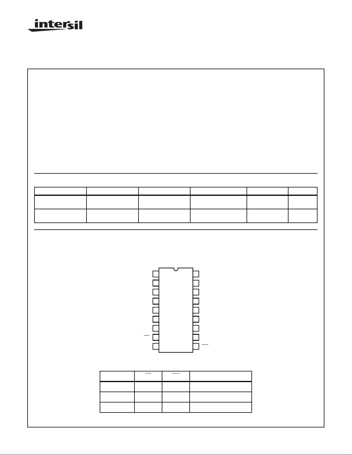
Pinout
MWS5114
(PDIP, SBDIP)
TOP VIEW
Description
The MWS5114 is a 1024 word by 4-bit static random access
memory that uses the ion-implanted silicon gate complementary MOS (CMOS) technology. It is designed for use in
memory systems where low power and simplicity in use are
desirable. This type has common data input and data output
and utilizes a single power supply of 4.5V to 6.5V.
The MWS5114 is supplied in 18 lead, hermetic, dual-in-line
sidebrazed ceramic packages (D suffix) and in 18 lead dualin-line plastic packages (E suffix).
E18.3
Burn-In
Burn-In
E18.3
D18.3
D18.3
1
A6
2
A5
3
A4
4
A3
5
A0
6
A1
7
A2
8
CS
9
V
SS
OPERATIONAL MODES
FUNCTION
Read 0 1 Output: Dependent on data
Write 0 0 Input
Not Selected 1 X High Impedance
CAUTION: These devices are sensitive to electrostatic discharge; follow proper IC Handling Procedures.
http://www.intersil.com or 407-727-9207
| Copyright © Intersil Corporation 1999
CS WE DATA PINS
6-160
18
V
DD
17
A7
16
A8
A9
15
14
I/O1
13
I/O2
12
I/O3
11
I/O4
10
WE
File Number 1325.2

Functional Block Diagram
A
4
A
5
A
6
A
7
A
8
A
9
I/O
1
I/O
2
MWS5114
ROW
SELECT
INPUT
DAT A
CONTROL
MEMORY ARRAY
64 ROWS
64 COLUMNS
COLUMN
I/O CIRCUITS
COLUMN SELECT
V
DD
V
SS
I/O
I/O
CS
WE
3
A
A
A
0
4
ENABLE
1
A
2
3
6-161
MWS5114
Absolute Maximum Ratings Thermal Information
DC Supply Voltage Range, (VDD)
(All Voltages Referenced to VSS Terminal). . . . . . . . -0.5V to +7V
Input Voltage Range, All Inputs . . . . . . . . . . . . .-0.5V to VDD +0.5V
DC Input Current, Any One Input. . . . . . . . . . . . . . . . . . . . . . . . .±10mA
Thermal Resistance (Typical) θJA (oC/W) θJC (oC/W)
Plastic DIP Package . . . . . . . . . . . . . . 75 N/A
SBDIP Package. . . . . . . . . . . . . . . . . . 75 20
Operating Temperature Range (TA)
Package Type D. . . . . . . . . . . . . . . . . . . . . . . . . .-55oC to +125oC
Package Type E. . . . . . . . . . . . . . . . . . . . . . . . . . .-40oC to +85oC
Maximum Storage Temperature Range (T
Maximum Junction Temperature
Ceramic Package . . . . . . . . . . . . . . . . . . . . . . . . . . . . . . . +175oC
Plastic Package. . . . . . . . . . . . . . . . . . . . . . . . . . . . . . . . .+150oC
Maximum Lead Temperature. . . . . . . . . . . . . . . . . . . . . . . . .+265oC
) . . .-65oC to +150oC
STG
Recommended Operating Conditions At T
PARAMETER
DC Operating Voltage Range 4.5 6.5 V
Input Voltage Range V
Static Electrical Specifications At T
CONDITIONS LIMITS
V
V
P ARAMETER SYMBOL
Quiescent
Device
Current
Output Low
(Sink) Current
Output High
(Source)
Current
IDD - 0, 5 5 - 75 100 - 75 100 - 75 250 µA
I
OL
I
OH
O
(V)
(V)
0.4 0, 5 5 2 4 - 2 4 - 2 4 - mA
4.6 0, 5 5 -0.4 -1 - -0.4 -1 - -0.4 -1 - mA
= 0oC to +70oC, VDD = ±5%, Except as Noted
A
V
IN
DD
(V)
= Full Package Temperature Range. For maximum reliability, operating
A
conditions should be selected so that operation is always within the following ranges:
LIMITS
ALL TYPES
MIN MAX
SS
MWS5114-3 MWS5114-2 MWS5114-1
MIN
(NOTE 1)
TYP MAX MIN
(NOTE 1)
TYP MAX MIN
V
DD
(NOTE 1)
TYP MAX
UNITS
V
UNITS
Output Voltage
Low-Level
Output Voltage
High-Level
Input Low
Voltage
Input High
Voltage
Input Leakage
Current (Note 2)
Operating
Current (Note 3)
VOL - 0, 5 5 - 0 0.1 - 0 0.1 - 0 0.1 V
VOH - 0, 5 5 4.9 5 - 4.9 5 - 4.9 5 - V
V
V
IIN - 0, 5 5 - ±0.1 ±5- ±0.1 ±5- ±0.1 ±5 µA
IDD1 - 0, 5 5 - 4 8 - 4 8 - 4 8 mA
0.5,
IL
0.5,
IH
- 5 - 1.2 0.8 - 1.2 0.8 - 1.2 0.8 V
4.5
- 5 2.4 - - 2.4 - - 2.4 - - V
4.5
6-162
 Loading...