


查询CMQ82C55AZ供应商
®
MS82C55A, MQ82C55A
Data Sheet June 28, 2005
CMOS Programmable Peripheral Interface
The Intersil 82C55A is a high performance CMOS version of
the industry standard 8255A and is manufactured using a
self-aligned silicon gate CMOS process (Scaled SAJI IV). It
is a general purpose programmable I/O device which may
be used with many different microprocessors. There are 24
I/O pins which may be individually programmed in two
groups of 12 and used in three major modes of operation.
The high performance and industry standard configuration of
the 82C55A make it compatible with the 80C86, 80C88 and
other microprocessors.
Static CMOS circuit design insures low operating power. The
Intersil advanced SAJI process results in performance equal
to or greater than existing functionally equivalent products at
a fraction of the power.
Ordering Information
PART
NUMBERS*
CMS82C55AZ
(Note)
IMS82C55AZ
(Note)
CMQ82C55AZ
(Note)
IMQ82C55AZ
(Note)
*Add “96” suffix to part number for tape and reel packaging.
TEMP.
RANGE (°C) PACKAGE PKG. DWG. #
0 to 70 44 Ld PLCC
(Pb-free)
-40 to 85
0 to 70 44 Ld MQFP
(Pb-free)
-40 to 85
N44.65
Q44.10x10
FN6140.1
Features
• Pb-Free Plus Anneal Available (RoHS Compliant)
(See Ordering Info)
• Pin Compatible with OKI MSM82C55A
- No Bus Hold Devices on any Port Pins
• 24 Programmable I/O Pins
• Fully TTL Compatible
• High Speed, No “Wait State” Operation with 8MHz 80C86
and 80C88
• Direct Bit Set/Reset Capability
• Enhanced Control Word Read Capability
• L7 Process
• 2.5mA Drive Capability on All I/O Ports
• Low Standby Power (ICCSB). . . . . . . . . . . . . . . . . . .10µA
NOTE: Intersil Pb-free plus anneal products employ special Pb-free
material sets; molding compounds/die attach materials and 100%
matte tin plate termination finish, which are RoHS compliant and
compatible with both SnPb and Pb-free soldering operations. Intersil
Pb-free products are MSL classified at Pb-free peak reflow
temperatures that meet or exceed the Pb-free requirements of
IPC/JEDEC J STD-020.
1
CAUTION: These devices are sensitive to electrostatic discharge; follow proper IC Handling Procedures.
1-888-INTERSIL or 1-888-468-3774
| Intersil (and design) is a registered trademark of Intersil Americas Inc.
All other trademarks mentioned are the property of their respective owners.
Copyright Intersil Americas Inc. 2005. All Rights Reserved

Pinouts
CS
GND
A1
A0
PC7
NC
PC6
PC5
PC4
PC0
PC1
MS82C55A (PLCC)
RD
PA0
PA1
7
8
9
10
11
12
13
14
15
16
17
PC2
PC3
PB0
TOP VIEW
PA2
PA3
NC
44 43 42 41 40
123456
NC
PB1
PB2
MS82C55A, MQ82C55A
MQ82C55A (MQFP)
TOP VIEW
PA4
PA5
PA6
PA7
WR
39
RESET
38
D0
D1
37
D2
36
D3
35
NC
34
D4
33
D5
32
D6
31
D7
30
V
29
CC
2827
262524232221201918
PB3
PB4
PB5
PB6
PB7
CS
GND
A1
A0
PC7
PC6
PC5
PC4
PC0
PC1
PC2
RD
PA0
PA1
44 43 42 41 40
1
2
3
4
5
6
7
8
9
10
11
12 13 14 15 16 17
NC
PA2
PA4
PA3
39 38 37 36 35 34
PA5
PA6
PA7
WR
33
32
31
30
29
28
27
26
25
24
23
2221201918
RESET
D0
D1
D2
D3
D4
D5
D6
D7
V
CC
PB7
NC
PC3
PB0
PB1
PB2
NC
PB3
PB4
PB5
Pin Description
SYMBOL TYPE DESCRIPTION
V
CC
GND GROUND
D0-D7 I/O DATA BUS: The Data Bus lines are bidirectional three-state pins connected to the system data bus.
RESET I RESET: A high on this input clears the control register and all ports (A, B, C) are set to the input mode.
CS
RD
WR
A0-A1 I ADDRESS: These input signals, in conjunction with the RD
PA0-PA7 I/O PORT A: 8-bit input and output port.
PB0-PB7 I/O PORT B: 8-bit input and output port.
PC0-PC7 I/O PORT C: 8-bit input and output port.
VCC: The +5V power supply pin. A 0.1µF capacitor between VCC and GND is recommended for decoupling.
I CHIP SELECT: Chip select is an active low input used to enable the 82C55A onto the Data Bus for CPU
communications.
I READ: Read is an active low input control signal used by the CPU to read status information or data via the data bus.
I WRITE: Write is an active low input control signal used by the CPU to load control words and data into the 82C55A.
and WR inputs, control the selection of one of the three
ports or the control word register. A0 and A1 are normally connected to the least significant bits of the Address Bus
A0, A1.
PB6
NC
2
FN6140.1
June 28, 2005
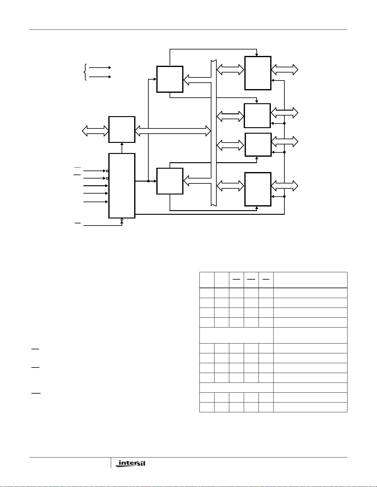
Functional Diagram
MS82C55A, MQ82C55A
POWER
SUPPLIES
BIDIRECTIONAL
DATA BUS
D7-D0
RD
WR
A1
A0
RESET
CS
+5V
GND
DATA BUS
BUFFER
READ
WRITE
CONTROL
LOGIC
GROUP A
CONTROL
8-BIT
INTERNAL
DATA BUS
GROUP B
CONTROL
FIGURE 1. FUNCTIONAL DIAGRAM
GROUP A
PORT A
(8)
GROUP A
PORT C
UPPER
(4)
GROUP B
PORT C
LOWER
(4)
GROUP B
PORT B
(8)
I/O
PA7 -PA0
I/O
PC7-PC4
I/O
PC3-PC0
I/O
PB7-PB0
Functional Description
Data Bus Buffer
This three-state bidirectional 8-bit buffer is used to interface
the 82C55A to the system data bus. Data is transmitted or
received by the buffer upon execution of input or output
instructions by the CPU. Control words and status
information are also transferred through the data bus buffer.
Read/Write and Control Logic
The function of this block is to manage all of the internal and
external transfers of both Data and Control or Status words.
It accepts inputs from the CPU Address and Control busses
and in turn, issues commands to both of the Control Groups.
(CS
) Chip Select. A “low” on this input pin enables the
communication between the 82C55A and the CPU.
(RD
) Read. A “low” on this input pin enables 82C55A to send
the data or status information to the CPU on the data bus. In
essence, it allows the CPU to “read from” the 82C55A.
(WR
) Write. A “low” on this input pin enables the CPU to
write data or control words into the 82C55A.
(A0 and A1) Port Select 0 and Port Select 1. These input
signals, in conjunction with the RD and WR inputs, control
the selection of one of the three ports or the control word
register. They are normally connected to the least significant
bits of the address bus (A0 and A1).
82C55A BASIC OPERATION
INPUT OPERATION
A1 A0 RD WR CS
(READ)
00010Port A → Data Bus
01010Port B → Data Bus
10010Port C → Data Bus
11010Control Word → Data Bus
OUTPUT OPERATION
(WRITE)
00100Data Bus → Port A
01100Data Bus → Port B
10100Data Bus → Port C
11100Data Bus → Control
DISABLE FUNCTION
XXXX1Data Bus → Three-State
XX110Data Bus → Three-State
(RESET) Reset. A “high” on this input initializes the control
register to 9Bh and all ports (A, B, C) are set to the input
mode.
3
FN6140.1
June 28, 2005
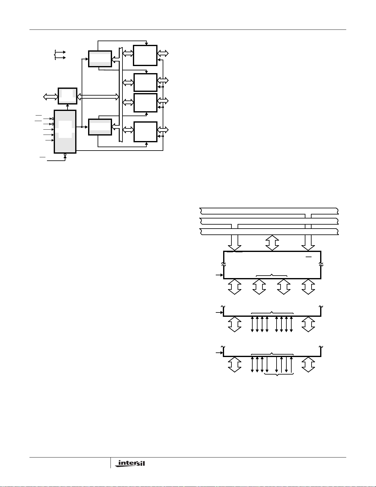
MS82C55A, MQ82C55A
I/O
PA7 -
POWER
SUPPLIES
BIDIRECTIONAL
DATA BUS
D7-D0
RD
WR
A1
A0
RESET
CONTROL
CS
+5V
GND
DATA
BUS
BUFFER
READ
WRITE
LOGIC
GROUP A
CONTROL
8-BIT
INTERNAL
DATA BUS
GROUP B
CONTROL
GROUP A
PORT A
(8)
GROUP A
PORT C
UPPER
(4)
GROUP B
PORT C
LOWER
(4)
GROUP B
PORT B
(8)
PA0
I/O
PC7-
PC4
I/O
PC3-
PC0
I/O
PB7-
PB0
FIGURE 2. 82C55A BLOCK DIAGRAM. DATA BUS BUFFER,
READ/WRITE, GROUP A & B CONTROL LOGIC
FUNCTIONS
Group A and Group B Controls
The functional configuration of each port is programmed by
the systems software. In essence, the CPU “outputs” a
control word to the 82C55A. The control word contains
information such as “mode”, “bit set”, “bit reset”, etc., that
initializes the functional configuration of the 82C55A.
contains a 4-bit latch and it can be used for the control signal
output and status signal inputs in conjunction with ports A
and B.
Operational Description
Mode Selection
There are three basic modes of operation than can be
selected by the system software:
Mode 0 - Basic Input/Output
Mode 1 - Strobed Input/Output
Mode 2 - Bidirectional Bus
When the reset input goes “high”, all ports will be set to the
input mode. After the reset is removed, the 82C55A can
remain in the input mode with no additional initialization
required. The control word register will contain 9Bh. During
the execution of the system program, any of the other modes
may be selected using a single output instruction. This
allows a single 82C55A to service a variety of peripheral
devices with a simple software maintenance routine. Any
port programmed as an output port is initialized to all zeros
when the control word is written.
ADDRESS BUS
CONTROL BUS
DATA BUS
Each of the Control blocks (Group A and Group B) accepts
“commands” from the Read/Write Control logic, receives
“control words” from the internal data bus and issues the
proper commands to its associated ports.
Control Group A - Port A and Port C upper (C7 - C4)
Control Group B - Port B and Port C lower (C3 - C0)
The control word register can be both written and read as
shown in the “Basic Operation” table. Figure 4 shows the
control word format for both Read and Write operations.
When the control word is read, bit D7 will always be a logic
“1”, as this implies control word mode information.
Ports A, B, and C
The 82C55A contains three 8-bit ports (A, B, and C). All can
be configured to a wide variety of functional characteristics
by the system software but each has its own special features
or “personality” to further enhance the power and flexibility of
the 82C55A.
Port A One 8-bit data output latch/buffer and one 8-bit data
input latch.
Port B One 8-bit data input/output latch/buffer and one 8-bit
data input buffer.
MODE 0
MODE 1
MODE 2
RD, WR
B
8I/O
PB7-PB0
B
8I/O
PB7-PB0 CONTROL
B
8I/O
PB7-PB0
D7-D0 A0-A1
82C55A
C
4I/O
PC3-PC0
OR I/O
PC7-PC4
C
CONTROL
OR I/O
C
CONTROL
4I/O
CS
A
8I/O
PA7 -PA0
A
8I/O
PA7 -PA0
A
PA7 -PA0
BIDIRECTIONAL
FIGURE 3. BASIC MODE DEFINITIONS AND BUS INTERFACE
Port C One 8-bit data output latch/buffer and one 8-bit data
input buffer (no latch for input). This port can be divided into
two 4-bit ports under the mode control. Each 4-bit port
4
FN6140.1
June 28, 2005
MS82C55A, MQ82C55A
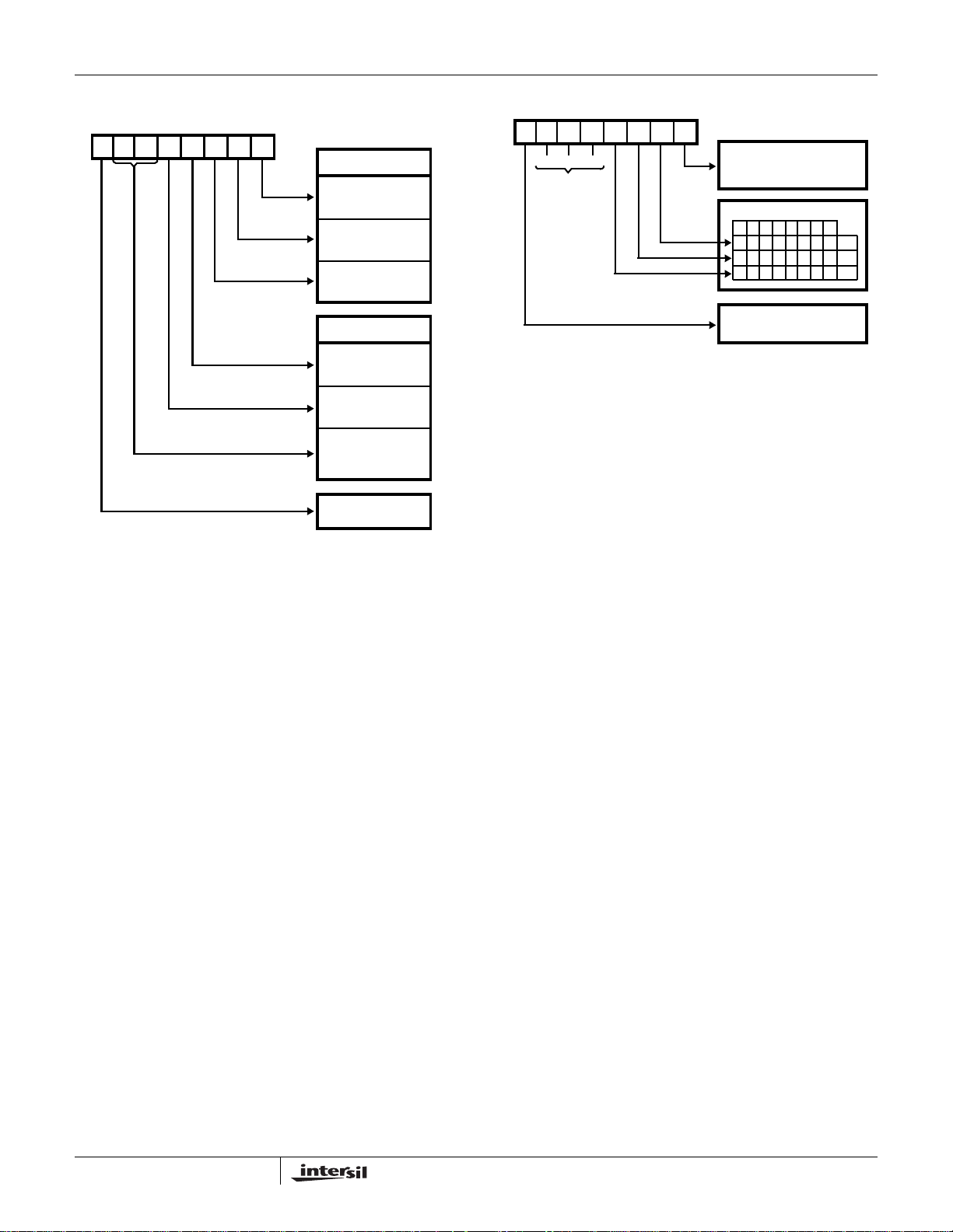
CONTROL WORD
D7 D6 D5 D4 D3 D2 D1 D0
FIGURE 4. MODE DEFINITION FORMAT
GROUP B
PORT C (LOWER)
1 = INPUT
0 = OUTPUT
PORT B
1 = INPUT
0 = OUTPUT
MODE SELECTION
0 = MODE 0
1 = MODE 1
GROUP A
PORT C (UPPER)
1 = INPUT
0 = OUTPUT
PORT A
1 = INPUT
0 = OUTPUT
MODE SELECTION
00 = MODE 0
01 = MODE 1
1X = MODE 2
MODE SET FLAG
1 = ACTIVE
The modes for Port A and Port B can be separately defined,
while Port C is divided into two portions as required by the
Port A and Port B definitions. All of the output registers,
including the status flip-flops, will be reset whenever the
mode is changed. Modes may be combined so that their
functional definition can be “tailored” to almost any I/O
structure. For instance: Group B can be programmed in
Mode 0 to monitor simple switch closings or display
computational results, Group A could be programmed in
Mode 1 to monitor a keyboard or tape reader on an interruptdriven basis.
The mode definitions and possible mode combinations may
seem confusing at first, but after a cursory review of the
complete device operation a simple, logical I/O approach will
surface. The design of the 82C55A has taken into account
things such as efficient PC board layout, control signal definition
vs. PC layout and complete functional flexibility to support
almost any peripheral device with no external logic. Such
design represents the maximum use of the available pins.
Single Bit Set/Reset Feature (Figure 5)
Any of the eight bits of Port C can be Set or Reset using a
single Output instruction. This feature reduces software
requirements in control-based applications.
CONTROL WORD
D7 D6 D5 D4 D3 D2 D1 D0
XXX
DON’T
CARE
FIGURE 5. BIT SET/RESET FORMAT
BIT SET/RESET
1 = SET
0 = RESET
BIT SELECT
1234567
0
01010101
00110011
00001111
BIT SET/RESET FLAG
0 = ACTIVE
B0
B1
B2
Interrupt Control Functions
When the 82C55A is programmed to operate in mode 1 or
mode 2, control signals are provided that can be used as
interrupt request inputs to the CPU. The interrupt request
signals, generated from port C, can be inhibited or enabled
by setting or resetting the associated INTE flip-flop, using
the bit set/reset function of port C.
This function allows the programmer to enable or disable a
CPU interrupt by a specific I/O device without affecting any
other device in the interrupt structure.
INTE Flip-Flop Definition
(BIT-SET)-INTE is SET - Interrupt Enable
(BIT-RESET)-INTE is Reset - Interrupt Disable
NOTE: All Mask flip-flops are automatically reset during mode
selection and device Reset.
Operating Modes
Mode 0 (Basic Input/Output). This functional configuration
provides simple input and output operations for each of the
three ports. No handshaking is required, data is simply
written to or read from a specific port.
Mode 0 Basic Functional Definitions:
• Two 8-bit ports and two 4-bit ports
• Any Port can be input or output
• Outputs are latched
• Inputs are not latched
• 16 different Input/Output configurations possible
When Port C is being used as status/control for Port A or B,
these bits can be set or reset by using the Bit Set/Reset
operation just as if they were output ports.
5
FN6140.1
June 28, 2005
MS82C55A, MQ82C55A
MODE 0 PORT DEFINITION
ABGROUP A#GROUP B
D4 D3 D1 D0 PORT A
PORT C
(Upper) PORT B
PORT C
(Lower)
0 0 0 0 Output Output 0 Output Output
0 0 0 1 Output Output 1 Output Input
0 0 1 0 Output Output 2 Input Output
0 0 1 1 Output Output 3 Input Input
0 1 0 0 Output Input 4 Output Output
0 1 0 1 Output Input 5 Output Input
0 1 1 0 Output Input 6 Input Output
0 1 1 1 Output Input 7 Input Input
Mode 0 (Basic Input)
RD
INPUT
tAR
CS
, A1, A0
tIR
MODE 0 PORT DEFINITION
A B GROUP A
GROUP B
PORT C
D4 D3 D1 D0 PORT A
(Upper) PORT B
#
1 0 0 0 Input Output 8 Output Output
1 0 0 1 Input Output 9 Output Input
1 0 1 0 Input Output 10 Input Output
1 0 1 1 Input Output 11 Input Input
1 1 0 0 Input Input 12 Output Output
1 1 0 1 Input Input 13 Output Input
1 1 1 0 Input Input 14 Input Output
1 1 1 1 Input Input 15 Input Input
tRR
tHR
tRA
PORT C
(Lower)
D7-D0
Mode 0 (Basic Output)
WR
D7-D0
CS
, A1, A0
OUTPUT
tAW
tRD tDF
tWW
tDW
tWD
tWA
tWB
6
FN6140.1
June 28, 2005
MS82C55A, MQ82C55A
Mode 0 Configurations
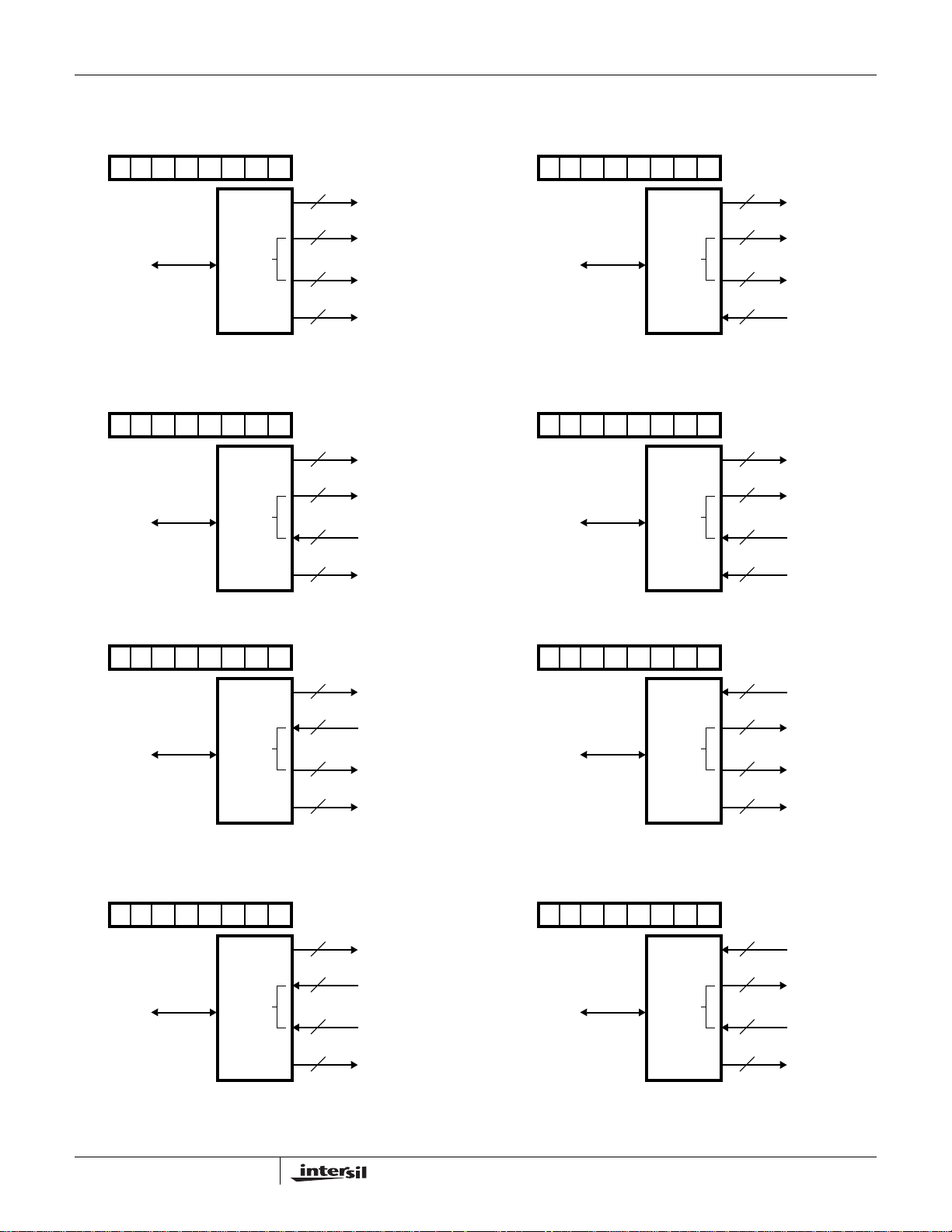
CONTROL WORD #0 CONTROL WORD #2
D0
1D70D60D50D40D30D20D10
82C55A
D7 - D0
8
4
4
PA7 - PA0
PC7 - PC4
PC3 - PC0
A
C
1D70D60D50D40D30D21D10
D7 - D0
82C55A
C
D0
8
4
4
PA7 - PA0
PC7 - PC4
PC3 - PC0
A
8
B
PB7 - PB0
CONTROL WORD #1 CONTROL WORD #3
D0
1D70D60D50D40D30D20D11
82C55A
D7 - D0
8
4
4
8
PA7 - PA0
PC7 - PC4
PC3 - PC0
PB7 - PB0
A
C
B
1D70D60D50D40D30D21D11
D7 - D0
CONTROL WORD #4 CONTROL WORD #8
D0
1D70D60D50D41D30D20D10
82C55A
D7 - D0
8
4
4
PA7 - PA0
PC7 - PC4
PC3 - PC0
A
C
1D70D60D51D40D30D20D10
D7 - D0
82C55A
C
82C55A
C
D0
D0
8
8
4
4
8
8
4
4
PB7 - PB0
PA7 - PA0
PC7 - PC4
PC3 - PC0
PB7 - PB0
PA7 - PA0
PC7 - PC4
PC3 - PC0
B
A
B
A
8
B
PB7 - PB0
CONTROL WORD #5 CONTROL WORD #9
D0
1D70D60D50D41D30D20D11
82C55A
D7 - D0
8
4
4
8
PA7 - PA0
PC7 - PC4
PC3 - PC0
PB7 - PB0
A
C
B
1D70D60D51D40D30D20D11
D7 - D0
7
82C55A
C
D0
8
8
4
4
8
PB7 - PB0
PA7 - PA0
PC7 - PC4
PC3 - PC0
PB7 - PB0
June 28, 2005
FN6140.1
B
A
B

MS82C55A, MQ82C55A
Mode 0 Configurations (Continued)
CONTROL WORD #6 CONTROL WORD #10
D0
1D70D60D50D41D30D21D10
82C55A
D7 - D0
8
4
4
PA7 - PA0
PC7 - PC4
PC3 - PC0
A
C
1D70D60D51D40D30D21D10
D7 - D0
82C55A
C
D0
8
4
4
PA7 - PA0
PC7 - PC4
PC3 - PC0
A
8
B
PB7 - PB0
CONTROL WORD #7 CONTROL WORD #11
D0
1D70D60D50D41D30D21D11
82C55A
D7 - D0
8
4
4
8
PA7 - PA0
PC7 - PC4
PC3 - PC0
PB7 - PB0
A
C
B
1D70D60D51D40D30D21D11
D7 - D0
CONTROL WORD #12 CONTROL WORD #14
D0
1D70D60D51D41D30D20D10
82C55A
D7 - D0
8
4
4
PA7 - PA0
PC7 - PC4
PC3 - PC0
A
C
1D70D60D51D41D30D21D10
D7 - D0
82C55A
C
82C55A
C
D0
D0
8
8
4
4
8
8
4
4
PB7 - PB0
PA7 - PA0
PC7 - PC4
PC3 - PC0
PB7 - PB0
PA7 - PA0
PC7 - PC4
PC3 - PC0
B
A
B
A
8
B
PB7 - PB0
CONTROL WORD #13 CONTROL WORD #15
D0
1D70D60D51D41D30D20D11
82C55A
D7 - D0
8
4
4
8
PA7 - PA0
PC7 - PC4
PC3 - PC0
PB7 - PB0
A
C
B
1D70D60D51D41D30D21D11
D7 - D0
8
82C55A
C
D0
8
8
4
4
8
PB7 - PB0
PA7 - PA0
PC7 - PC4
PC3 - PC0
PB7 - PB0
June 28, 2005
FN6140.1
B
A
B

MS82C55A, MQ82C55A
Operating Modes
Mode 1 - (Strobed Input/Output). This functional configuration
provides a means for transferring I/O data to or from a specified
port in conjunction with strobes or “hand shaking” signals. In
mode 1, port A and port B use the lines on port C to generate or
accept these “hand shaking” signals.
Mode 1 Basic Function Definitions:
• Two Groups (Group A and Group B)
• Each group contains one 8-bit port and one 4-bit control/data
port
• The 8-bit data port can be either input or output. Both inputs
and outputs are latched.
• The 4-bit port is used for control and status of the 8-bit port.
Input Control Signal Definition
(Figures 6 and 7)
STB (Strobe Input)
A “low” on this input loads data into the input latch.
IBF (Input Buffer Full F/F)
A “high” on this output indicates that the data has been loaded
into the input latch: in essence, an acknowledgment. IBF is set
by STB input being low and is reset by the rising edge of the
RD
input.
INTR (Interrupt Request)
A “high” on this output can be used to interrupt the CPU when
an input device is requesting service. INTR is set by the
condition: STB
is reset by the falling edge of RD
is a “one”, IBF is a “one” and INTE is a “one”. It
. This procedure allows an
input device to request service from the CPU by simply strobing
its data into the port.
INTE A
Controlled by bit set/reset of PC4.
INTE B
Controlled by bit set/reset of PC2.
Output Control Signal Definition
(Figure 8 and 9)
OBF - (Output Buffer Full F/F). The OBF output will go “low”
to indicate that the CPU has written data out to the specified
port. This does not mean valid data is sent out of the port at this
time since OBF
guaranteed valid at the rising edge of OBF
OBF
F/F will be set by the rising edge of the WR input and reset
by ACK
can go true before data is available. Data is
, (See Note 1). The
input being low.
CONTROL WORD
1D70D61D51D41/0
INTR
D3
STB
IBF
RD
D2 D1 D0
PC6, PC7
1 = INPUT
0 = OUTPUT
RD
MODE 1 (PORT A)
PA7 -PA0
INTE
A
PC4
PC3
PC6, PC7
tSIB
8
STBA
IBFAPC5
INTRA
2
I/O
FIGURE 6. MODE 1 INPUT
tST
tSIT
tPH
CONTROL WORD
D7
D6 D5 D4 D3 D2 D1 D0
1
tRIT
11
RD
MODE 1 (PORT B)
INTE
B
tRIB
PB7-PB0
PC2
PC0
8
STBB
IBFBPC1
INTRB
INPUT FROM
PERIPHERAL
tPS
FIGURE 7. MODE 1 (STROBED INPUT)
9
FN6140.1
June 28, 2005

MS82C55A, MQ82C55A
ACK - (Acknowledge Input). A “low” on this input informs the
82C55A that the data from Port A or Port B is ready to be
accepted. In essence, a response from the peripheral device
indicating that it is ready to accept data, (See Note 1).
INTR - (Interrupt Request). A “high” on this output can be
used to interrupt the CPU when an output device has
accepted data transmitted by the CPU. INTR is set when
ACK
is a “one”, OBF is a “one” and INTE is a “one”. It is reset
by the falling edge of WR
.
INTE A
Controlled by Bit Set/Reset of PC6.
INTE B
Controlled by Bit Set/Reset of PC2.
NOTE:
1. To strobe data into the peripheral device, the user must operate
the strobe line in a hand shaking mode. The user needs to send
OBF
to the peripheral device, generates an ACK from the
peripheral device and then latch data into the peripheral device
on the rising edge of OBF
WR
.
tWOB
CONTROL WORD
1D70D61D51D41/0
CONTROL WORD
D7
D6 D5 D4 D3 D2 D1 D0
1
D3
D2 D1 D0
10
FIGURE 8. MODE 1 OUTPUT
PC4, PC5
1 = INPUT
0 = OUTPUT
WR
WR
MODE 1 (PORT A)
PA7 -PA0
PC7
INTE
A
PC3
PC4, PC5
MODE 1 (PORT B)
PB7-PB0
PC1
INTE
B
PC0
8
OBFA
ACKAPC6
INTRA
2
8
OBFB
ACKBPC2
INTRB
OBF
INTR
ACK
OUTPUT
tWIT
tWB
tAOB
tAK tAIT
FIGURE 9. MODE 1 (STROBED OUTPUT)
PC7
PC6
PC3
PC2
PC1
PC0
8
2
8
OBFA
ACKA
INTRA
I/O
STBB
IBFB
INTRB
CONTROL WORD
1D70D61D51D41/0
PC4
PC5
PC3
PC1
PC2
PC0
8
2
8
STBA
IIBFA
INTRA
I/O
OBFB
ACKB
INTRB
CONTROL WORD
PA7 -PA0
RD
D3
D2 D1 D0
10 1D70D61D50D41/0
PC6, PC7
1 = INPUT
0 = OUTPUT
WR
PORT A - (STROBED INPUT)
PORT B - (STROBED OUTPUT)
PC6, PC7
PB7, PB0
D3
WR
D2 D1 D0
11
PC4, PC5
1 = INPUT
0 = OUTPUT
RD
PA7 -PA0
PC4, PC5
PB7, PB0
PORT A - (STROBED OUTPUT)
PORT B - (STROBED INPUT)
Combinations of Mode 1: Port A and Port B can be individually defined as input or output in Mode 1 to support a wide variety of strobed I/O applications.
FIGURE 10. COMBINATIONS OF MODE 1
10
FN6140.1
June 28, 2005

MS82C55A, MQ82C55A
Operating Modes
Mode 2 (Strobed Bidirectional Bus I/O)
This functional configuration provides a means for
communicating with a peripheral device or structure on a
single 8-bit bus for both transmitting and receiving data
(bidirectional bus I/O). “Hand shaking” signals are provided to
maintain proper bus flow discipline similar to Mode 1. Interrupt
generation and enable/disable functions are also available.
Mode 2 Basic Functional Definitions:
• Used in Group A only
• One 8-bit, bidirectional bus Port (Port A) and a 5-bit
control Port (Port C)
• Both inputs and outputs are latched
• The 5-bit control port (Port C) is used for control and
status for the 8-bit, bidirectional bus port (Port A)
Bidirectional Bus I/O Control Signal Definition
(Figures 11, 12, 13, 14)
INTR - (Interrupt Request). A high on this output can be
used to interrupt the CPU for both input or output operations.
ONTROL WORD
D7
D6 D5 D4 D3 D2 D1 D0
1
1/0 1/011/0
Output Operations
OBF - (Output Buffer Full). The OBF output will go “low” to
indicate that the CPU has written data out to port A.
ACK
- (Acknowledge). A “low” on this input enables the threestate output buffer of port A to send out the data. Otherwise,
the output buffer will be in the high impedance state.
INTE 1 - (The INTE flip-flop associated with OBF
).
Controlled by bit set/reset of PC4.
Input Operations
STB - (Strobe Input). A “low” on this input loads data into the
input latch.
IBF - (Input Buffer Full F/F). A “high” on this output indicates
that data has been loaded into the input latch.
INTE 2 - (The INTE flip-flop associated with IBF). Controlled
by bit set/reset of PC4.
PC3
PA7 -PA0
INTRA
8
PC2-PC0
1 = INPUT
0 = OUTPUT
PORT B
1 = INPUT
0 = OUTPUT
GROUP B MODE
0 = MODE 0
1 = MODE 1
FIGURE 11. MODE CONTROL WORD FIGURE 12. MODE 2
WR
RD
INTE
1
INTE
2
PC2-PC0
PC7
PC6
PC4
PC5
3
OBFA
ACKA
STB
IBFA
I/O
A
11
FN6140.1
June 28, 2005

WR
OBF
INTR
ACK
STB
MS82C55A, MQ82C55A
DATA FROM
CPU TO 82C55A
tAOB
tWOB
tAK
tST
IBF
PERIPHERAL
BUS
RD
DATA FROM
PERIPHERAL TO 82C55A
tSIB
tPS
tPH
tAD
DATA FROM
82C55A TO PERIPHERAL
tKD
tRIB
DATA FROM
82C55A TO CPU
NOTE: Any sequence where WR occurs before ACK and STB occurs before RD is permissible. (INTR = IBF • MASK • STB • RD + OBF • MASK
• ACK
• WR)
FIGURE 13. MODE 2 (BIDIRECTIONAL)
MODE 2 AND MODE 0 (INPUT) MODE 2 AND MODE 0 (OUTPUT)
CONTROL WORD
D5 D4 D3 D2 D1 D0
D6
1D71
01
PC2-PC0
1 = INPUT
0 = OUTPUT
RD
WR
1/0
PC3
PA7 -PA0
PC7
PC6
PC4
PC5
PC2-PC0
PB7-PB0
8
3
8
INTRA
OBFA
ACKA
STBA
IBFA
I/O
CONTROL WORD
D5 D4 D3 D2 D1 D0
D6
1D71
00
PC2-PC0
1 = INPUT
0 = OUTPUT
RD
WR
1/0
PC3
PA7 -PA0
PC7
PC6
PC4
PC5
PC2-PC0
PB7, PB0
8
3
8
INTRA
OBFA
ACKA
STBA
IBFA
I/O
12
FIGURE 14. MODE 2 COMBINATIONS
FN6140.1
June 28, 2005

MS82C55A, MQ82C55A
MODE 2 AND MODE 1 (OUTPUT) MODE 2 AND MODE 1 (INPUT)
CONTROL WORD
D6
D5 D4 D3 D2 D1 D0
1D71
PA0
PA1
PA2
PA3
PA4
PA5
PA6
PA7
PB0
PB1
PB2
PB3
PB4
PB5
PB6
PB7
PC0
PC1
PC2
PC3
PC4
PC5
PC6
PC7
10
RD
WR
PC3
PA7 -PA0
PC7
PC6
PC4
PC5
PB7-PB0
PC1
PC2
PC0
8
8
INTRA
OBFA
ACKA
STBA
IBFA
OBFB
ACKB
INTRB
CONTROL WORD
D6
D5 D4 D3 D2 D1 D0
D7
1
1
PA7 -PA0
11
PB7-PB0
RD
WR
FIGURE 14. MODE 2 COMBINATIONS (Continued)
MODE DEFINITION SUMMARY
MODE 0 MODE 1 MODE 2
IN OUT IN OUT GROUP A ONLY
In
In
In
In
In
In
In
In
In
In
In
In
In
In
In
In
In
In
In
In
In
In
In
In
Out
Out
Out
Out
Out
Out
Out
Out
Out
Out
Out
Out
Out
Out
Out
Out
Out
Out
Out
Out
Out
Out
Out
Out
In
In
In
In
In
In
In
In
In
In
In
In
In
In
In
In
INTRB
IBFB
STB
INTRA
STB
IBFA
I/O
I/O
B
A
Out
Out
Out
Out
Out
Out
Out
Out
Out
Out
Out
Out
Out
Out
Out
Out
INTRB
OBF
ACK
INTRA
I/O
I/O
ACK
OBF
I/O
B
B
I/O
I/O
INTRA
STB
A
IBFA
A
A
ACK
OBF
A
A
PC3
PC7
PC6
PC4
PC5
PC2
PC1
PC0
INTRA
8
OBFA
ACKA
STBA
IBFA
8
STBB
IBFB
INTRB
Mode 0
or Mode 1
Only
13
FN6140.1
June 28, 2005

MS82C55A, MQ82C55A
Special Mode Combination Considerations
There are several combinations of modes possible. For any
combination, some or all of Port C lines are used for control
or status. The remaining bits are either inputs or outputs as
defined by a “Set Mode” command.
During a read of Port C, the state of all the Port C lines,
except the ACK
bus. In place of the ACK
appear on the data bus in the PC2, PC4, and PC6 bit
positions as illustrated by Figure 17.
Through a “Write Port C” command, only the Port C pins
programmed as outputs in a Mode 0 group can be written.
No other pins can be affected by a “Write Port C” command,
nor can the interrupt enable flags be accessed. To write to
any Port C output programmed as an output in Mode 1
group or to change an interrupt enable flag, the “Set/Reset
Port C Bit” command must be used.
With a “Set/Reset Port C Bit” command, any Port C line
programmed as an output (including IBF and OBF
written, or an interrupt enable flag can be either set or reset.
Port C lines programmed as inputs, including ACK
lines, associated with Port C are not affected by a “Set/Reset
Port C Bit” command. Writing to the corresponding Port C bit
positions of the ACK
C Bit” command will affect the Group A and Group B
interrupt enable flags, as illustrated in Figure 17.
D7 D6 D5 D4 D3 D2 D1 D0
I/O I/O IBFA INTEA INTRA INTEB IBFB INTRB
D7 D6 D5 D4 D3 D2 D1 D0
OBFA INTEA I/O I/O INTRA INTEB OBFB INTRB
FIGURE 15. MODE 1 STATUS WORD FORMAT
D7 D6 D5 D4 D3 D2 D1 D0
OBFA INTE1 IBFA INTE2 INTRA X X X
and STB lines, will be placed on the data
and STB line states, flag status will
and STB lines with the “Set Reset Port
INPUT CONFIGURATION
GROUP A
OUTPUT CONFIGURATION
GROUP A
GROUP A
(Defined by Mode 0 or Mode 1 Selection)
GROUP B
GROUP B
GROUP B
) can be
and STB
Current Drive Capability
Any output on Port A, B or C can sink or source 2.5mA. This
feature allows the 82C55A to directly drive Darlington type
drivers and high-voltage displays that require such sink or
source current.
Reading Port C Status (Figures 15 and 16)
In Mode 0, Port C transfers data to or from the peripheral
device. When the 82C55A is programmed to function in
Modes 1 or 2, Port C generates or accepts “hand shaking”
signals with the peripheral device. Reading the contents of
Port C allows the programmer to test or verify the “status” of
each peripheral device and change the program flow
accordingly.
There is not a special instruction to read the status
information from Port C. A normal read operation of Port C is
executed to perform this function.
INTERRUPT
ENABLE FLAG POSITION
INTE B PC2 ACK
INTE A2 PC4 STBA (Input Mode 1 or Mode 2)
INTE A1 PC6 ACK
FIGURE 17. INTERRUPT ENABLE FLAGS IN MODES 1 AND 2
ALTERNATE PORT C
PIN SIGNAL (MODE)
B (Output Mode 1)
or STB
B (Input Mode 1)
A (Output Mode 1 or Mode 2)
Applications of the 82C55A
The 82C55A is a very powerful tool for interfacing peripheral
equipment to the microcomputer system. It represents the
optimum use of available pins and is flexible enough to
interface almost any I/O device without the need for
additional external logic.
Each peripheral device in a microcomputer system usually
has a “service routine” associated with it. The routine
manages the software interface between the device and the
CPU. The functional definition of the 82C55A is programmed
by the I/O service routine and becomes an extension of the
system software. By examining the I/O devices interface
characteristics for both data transfer and timing, and
matching this information to the examples and tables in the
detailed operational description, a control word can easily be
developed to initialize the 82C55A to exactly “fit” the
application. Figures 18 through 24 present a few examples
of typical applications of the 82C55A.
FIGURE 16. MODE 2 STATUS WORD FORMAT
14
FN6140.1
June 28, 2005

MS82C55A, MQ82C55A
INTERRUPT
REQUEST
PC3
MODE 1
(OUTPUT)
82C55A
MODE 1
(OUTPUT)
PC0
INTERRUPT
REQUEST
FIGURE 18. PRINTER INTERFACE
INTERRUPT
REQUEST
PC3
PA0
PA1
PA2
PA3
PA4
PA5
PA6
PA7
PC4
PC5
PB0
PB1
PB2
PB3
PB4
PB5
PB6
PB7
PC1
PC2
PC6
PC7
(OUTPUT)
INTERRUPT
REQUEST
MODE 1
(INPUT)
82C55A
MODE 1
FIGURE 19. KEYBOARD AND DISPLAY INTERFACE
R0
R1
R2
R3
R4
R5
SHIFT
CONTROL
STROBE
ACK
B0
B1
B2
B3
B4
B5
BACKSPACE
CLEAR
DATA READY
ACK
BLANKING
CANCEL WORD
FULLY
DECODED
KEYBOARD
BURROUGHS
SELF-SCAN
DISPLAY
PA0
PA1
PA2
PA3
PA4
PA5
PA6
PA7
PC7
PC6
PC5
PC4
PB0
PB1
PB2
PB3
PB4
PB5
PB6
PB7
PC1
PC2
DATA READY
ACK
PAP ER F EED
FORWARD/REV.
DATA READY
ACK
CONTROL LOGIC
AND DRIVERS
INTERRUPT
REQUEST
FIGURE 20. KEYBOARD AND TERMINAL ADDRESS
HIGH SPEED
PRINTER
HAMMER
RELAYS
PAP ER F EE D
FORWARD/REV.
RIBBON
CARRIAGE SEN.
PC3
PA0
PA1
PA2
PA3
PA4
MODE 1
(INPUT)
82C55A
MODE 0
(INPUT)
PA5
PA6
PA7
PC4
PC5
PC6
PC7
PB0
PB1
PB2
PB3
PB4
PB5
PB6
PB7
INTERFACE
R0
R1
R2
R3
R4
KEYBOARD
R5
SHIFT
CONTROL
STROBE
ACK
BUST LT
TEST LT
FULLY
DECODED
TERMINAL
ADDRESS
15
FN6140.1
June 28, 2005

MODE 0
(OUTPUT)
82C55A
BIT
SET/RESET
MODE 0
(INPUT)
PA0
PA1
PA2
PA3
PA4
PA5
PA6
PA7
PC4
PC5
PC6
PC7
PC0
PC1
PC2
PC3
PB0
PB1
PB2
PB3
PB4
PB5
PB6
PB7
LSB
12-BIT
D/A
CONVERTER
(DAC)
MSB
STB DATA
SAMPLE EN
STB
LSB
8-BIT
A/D
CONVERTER
(ADC)
MSB
MS82C55A, MQ82C55A
INTERRUPT
REQUEST
MODE 1
ANALOG
OUTPUT
ANALOG
INPUT
(OUTPUT)
MODE 0
(OUTPUT)
PC3
82C55A
PA0
PA1
PA2
PA3
PA4
PA5
PA6
PA7
PC7
PC6
PC5
PC4
PC2
PC1
PC0
PB0
PB1
PB2
PB3
PB4
PB5
PB6
PB7
R0
R1
R2
CRT CONTROLLER
R3
² CHARACTER GEN.
² REFRESH BUFFER
R4
² CURSOR CONTROL
R5
SHIFT
CONTROL
DATA READY
ACK
BLANKED
BLACK/WHITE
ROW STB
COLUMN STB
CURSOR H/V STB
CURSOR/ROW/COLUMN
ADDRESS
H&V
FIGURE 21. DIGITAL TO ANALOG, ANALOG TO DIGITAL FIGURE 22. BASIC CRT CONTROLLER INTERFACE
INTERRUPT
REQUEST
(OUTPUT)
PC3
MODE 2
82C55A
MODE 0
PA0
PA1
PA2
PA3
PA4
PA5
PA6
PA7
PC4
PC5
PC7
PC6
PC2
PC1
PC0
PB0
PB1
PB2
PB3
PB4
PB5
PB6
PB7
D0
D1
D2
D3
D4
D5
D6
D7
DATA STB
ACK (IN)
DATA READY
ACK (OUT)
TRACK “0” SENSOR
SYNC READY
INDEX
ENGAGE HEAD
FORWARD/REV.
READ ENABLE
WRITE ENABLE
DISC SELECT
ENABLE CRC
TEST
BUSY LT
FLOPPY DISK
CONTROLLER
AND DRIVE
INTERRUPT
REQUEST
(OUTPUT)
PC3
MODE 1
(INPUT)
82C55A
MODE 0
(INPUT)
MODE 0
PA0
PA1
PA2
PA3
PA4
PA5
PA6
PA7
PC4
PC5
PC6
PC0
PC1
PC2
PB0
PB1
PB2
PB3
PB4
PB5
PB6
PB7
R0
R1
R2
B LEVEL
R3
PAPER
R4
TAP E
READER
R5
R6
R7
STB
ACK
STOP/GO
MACHINE TOOL
START/STOP
LIMIT SENSOR (H/V)
OUT OF FLUID
CHANGE TOOL
LEFT/RIGHT
UP/DOWN
HOR. STEP STROBE
VERT. STEP STROBE
SLEW/STEP
FLUID ENABLE
EMERGENCY STOP
FIGURE 23. BASIC FLOPPY DISC INTERFACE FIGURE 24. MACHINE TOOL CONTROLLER INTERFACE
16
FN6140.1
June 28, 2005

MS82C55A, MQ82C55A
Absolute Maximum Ratings T
Supply Voltage. . . . . . . . . . . . . . . . . . . . . . . . . . . . . . . . . . . . . +8.0V
Input, Output or I/O Voltage. . . . . . . . . . . . GND-0.5V to V
ESD Classification . . . . . . . . . . . . . . . . . . . . . . . . . . . . . . . . Class 1
= 25°C Thermal Information
A
Thermal Resistance (Typical, Note 1) θ
+0.5V
CC
PLCC Package. . . . . . . . . . . . . . . . . . . . . . . . . . . . . . . . . . . 55
MQFP Package . . . . . . . . . . . . . . . . . . . . . . . . . . . . . . . . . . 62
JA
(°C/W)
Maximum Storage Temperature Range . . . . . . . . . . -65°C to 150°C
Operating Conditions
Voltage Range . . . . . . . . . . . . . . . . . . . . . . . . . . . . . . . +4.5V to 5.5V
Operating Temperature Range
CMX82C55A . . . . . . . . . . . . . . . . . . . . . . . . . . . . . . . 0°C to 70°C
Maximum Junction Temperature
Plastic Packages . . . . . . . . . . . . . . . . . . . . . . . . . . . . . . . . 150°C
Maximum Lead Temperature (Soldering 10s) . . . . . . . . . . . . 300°C
(Lead Tips Only)
IMX82C55A . . . . . . . . . . . . . . . . . . . . . . . . . . . . . . -40°C to 85°C
Die Characteristics
Gate Count . . . . . . . . . . . . . . . . . . . . . . . . . . . . . . . . . . 1000 Gates
CAUTION: Stresses above those listed in “Absolute Maximum Ratings” may cause permanent damage to the device. This is a stress only rating and operation of the
device at these or any other conditions above those indicated in the operational sections of this specification is not implied.
NOTE:
is measured with the component mounted on an evaluation PC board in free air.
1. θ
JA
Electrical Specifications V
SYMBOL PARAMETER TEST CONDITIONS MIN TYP MAX UNITS
V
V
V
IDAR Darlington Drive Current Ports A, B, C. Test Condition 3 -2.5 - Notes 2, 4 mA
ICCSB Standby Power Supply Current V
ICCOP Operating Power Supply Current T
NOTES:
2. No internal current limiting exists on Port Outputs. A resistor must be added externally to limit the current.
3. ICCOP = 1mA/MHz of Peripheral Read/Write cycle time. (Example: 1.0µs I/O Read/Write cycle time = 1mA).
4. Tested as V
Logical One Input Voltage 2.0
IH
V
Logical Zero Input Voltage - - 0.8 V
IL
Logical One Output Voltage IOH = -2.5mA,
OH
Logical Zero Output Voltage IOL +2.5mA - - 0.4 V
OL
I
Input Leakage Current VIN = VCC or GND, RD, CS, A1, A0, RESET, WR -1.0 - +1.0 µA
I
IO I/O Pin Leakage Current VO = V
at -2.5mA.
OH
= 5.0V± 10%; TA = Operating Temperature Range
CC
I
= -100µA
OH
or GND, D0 - D7 -10 - +10 µA
CC
= 5.5V, VIN = VCC or GND. Output Open - - 10 µA
CC
= +25°C, VCC = 5.0V, Typical (See Note 3) - 1 - mA/MHz
A
2.2
3.0
VCC -0.4
--V
--V
Capacitance T
= 25°C
A
SYMBOL PARAMETER TYPICAL UNITS TEST CONDITIONS
CIN Input Capacitance 10 pF FREQ = 1MHz, All Measurements are referenced to
CI/O I/O Capacitance 20 pF
device GND
17
FN6140.1
June 28, 2005

MS82C55A, MQ82C55A
AC Electrical Specifications V
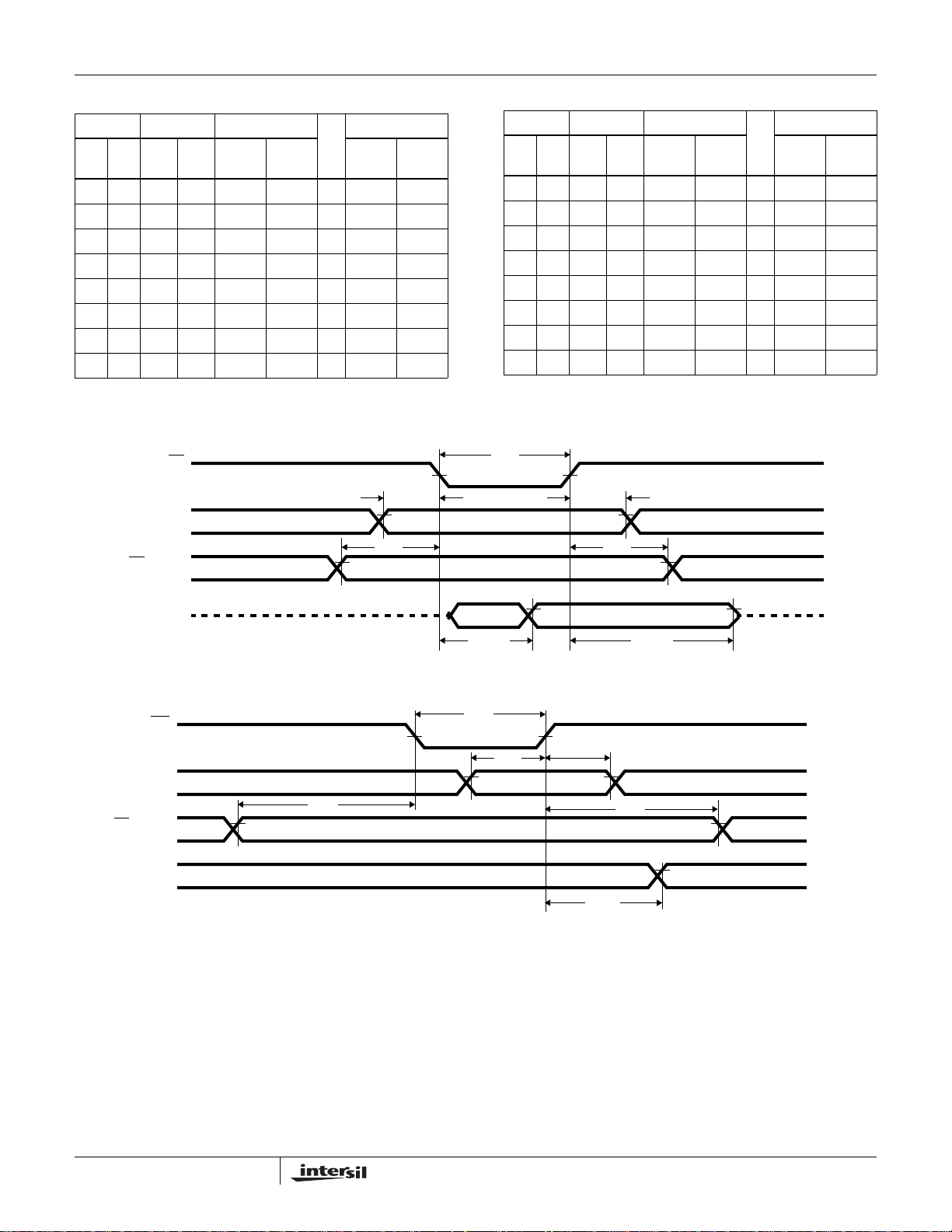
SYMBOL PARAMETER
READ TIMING
(1) tAR Address Stable Before RD
(2) tRA Address Stable After RD
(3) tRR RD Pulse Width 150 - ns
(4) tRD Data Valid From RD
(5) tDF Data Float After RD
(6) tRV Time Between RDs and/or WRs 300 - ns
WRITE TIMING
(7) tAW Address Stable Before WR
(8) tWA Address Stable After WR 20 - ns
(9) tWW WR
(10) tDW Data Valid to WR
(11) tWD Data Valid After WR High 30 - ns
OTHER TIMING
(12) tWB WR
(13) tIR Peripheral Data Before RD
(14) tHR Peripheral Data After RD 0-ns
(15) tAK ACK Pulse Width 200 - ns
(16) tST STB Pulse Width 100 - ns
(17) tPS Peripheral Data Before STB High 20 - ns
(18) tPH Peripheral Data After STB High 50 - ns
(19) tAD ACK = 0 to Output 1 - 175 ns
(20) tKD ACK = 1 to Output Float 2 20 250 ns
(21) tWOB WR
(22) tAOB ACK = 0 to OBF = 1 1 - 150 ns
(23) tSIB STB = 0 to IBF = 1 1 - 150 ns
(24) tRIB RD
(25) tRIT RD
(26) tSIT STB = 1 to INTR = 1 1 - 150 ns
(27) tAIT ACK = 1 to INTR = 1 1 - 150 ns
(28) tWIT WR
(29) tRES Reset Pulse Width 1, (Note) 500 - ns
NOTE: Period of initial Reset pulse after power-on must be at least 50µsec. Subsequent Reset pulses may be 500ns minimum.
Pulse Width 100 - ns
= 1 to Output 1 - 350 ns
= 1 to OBF = 0 1 - 150 ns
= 1 to IBF = 0 1 - 150 ns
= 0 to INTR = 0 1 - 200 ns
= 0 to INTR = 0 1 - 200 ns
= +5V± 10%, GND = 0V; TA = Operating Temperature Range
CC
TEST
CONDITIONS
1 - 120 ns
21075ns
High 100 - ns
82C55A
UNITSMIN MAX
0-ns
0-ns
0-ns
0-ns
18
FN6140.1
June 28, 2005

Timing Waveforms
MS82C55A, MQ82C55A
CS
CS
RD
INPUT
, A1, A0
D7-D0
WR
D7-D0
, A1, A0
tAW (7)
tRR (3)
tIR (13)
tAR (1)
tRD (4) tDF (5)
FIGURE 25. MODE 0 (BASIC INPUT)
tWW (9)
tDW
(10)
tHR (14)
tRA (2)
tWD (11)
tWA (8)
OUTPUT
STB
IBF
INTR
RD
INPUT FROM
PERIPHERAL
FIGURE 26. MODE 0 (BASIC OUTPUT)
tST (16)
tSIB
(23)
tPS (17)
tSIT
(26)
tPH
(18)
FIGURE 27. MODE 1 (STROBED INPUT)
tRIT
(25)
tWS (12)
tRIB (24)
19
FN6140.1
June 28, 2005

Timing Waveforms (Continued)
WR
OBF
MS82C55A, MQ82C55A
tWOB (21)
tAOB (22)
INTR
ACK
OUTPUT
WR
OBF
INTR
ACK
DATA FROM
CPU TO 82C55A
tWIT
(28)
tAK (15) tAIT (27)
tWB (12)
FIGURE 28. MODE 1 (STROBED OUTPUT)
tWOB
(21)
tAOB
(22)
tAK
(15)
(NOTE)
STB
IBF
PERIPHERAL
BUS
RD
NOTE: Any sequence where WR
• ACK
• WR)
20
tST
(16)
(NOTE)
tSIB
(23)
tPS (17)
tPH (18)
DATA FROM
PERIPHERAL TO 82C55A
tAD (19)
DATA FROM
82C55A TO PERIPHERAL
tKD
(20)
tRIB (24)
DATA FROM
82C55A TO CPU
FIGURE 29. MODE 2 (BIDIRECTIONAL)
occurs before ACK and STB occurs before RD is permissible. (INTR = IBF • MASK • STB • RD + OBF • MASK
FN6140.1
June 28, 2005

Timing Waveforms (Continued)
A
MS82C55A, MQ82C55A
A0-A1,
CS
DATA
BUS
WR
tAW (7)
tWA (8)
tDW (10) tWD (11)
tWW (9)
A0-A1,
CS
RD
DATA
BUS
tAR (1)
tRR (3)
(4) tRD
VAL ID
HIGH IMPEDANCE
FIGURE 30. WRITE TIMING FIGURE 31. READ TIMING
AC Test Circuit AC Testing Input, Output Waveforms
V1
R1
OUTPUT FROM
DEVICE UNDER
TEST
R2
NOTE: Includes STRAY and JIG Capacitance
C1
(SEE NOTE)
TEST
POINT
INPUT
VIH + 0.4V
1.5V 1.5V
VIL - 0.4V
C Testing: All AC Parameters tested as per test circuits. Input RISE
and FALL times are driven at 1ns/V.
TEST CONDITION DEFINITION TABLE
TEST CONDITION V1 R1 R2 C1
1 1.7V 523Ω Open 150pF
2V
CC
2kΩ 1.7kΩ 50pF
3 1.5V 750Ω Open 50pF
tRA (2)
tDF (5)
OUTPUT
VOH
VOL
21
FN6140.1
June 28, 2005

MS82C55A, MQ82C55A
Die Characteristics
METALLIZATION:
Type: Silicon - Aluminum
Thickness: 11kÅ ±1kÅ
Metallization Mask Layout
CS
GND
A1
A0
PC7
GLASSIVATION:
Type: SiO
2
Thickness: 8kÅ ±1kÅ
82C55A
RD PA0 PA1 PA2 PA3 PA4 PA5 PA6 PA7 WR
RESET
D0
D1
D2
D3
D4
PC6
PC5
PC4
PC0
PC1
PC2 PC3 PB0 PB1 PB2 PB3 PB4 PB5 PB6 PB7
D5
D6
D7
V
CC
22
FN6140.1
June 28, 2005

MS82C55A, MQ82C55A
Plastic Leaded Chip Carrier Packages (PLCC)
0.042 (1.07)
0.048 (1.22)
PIN (1) IDENTIFIER
0.020 (0.51) MAX
3 PLCS
C
L
D1
D
0.026 (0.66)
0.032 (0.81)
0.045 (1.14)
MIN
0.042 (1.07)
0.056 (1.42)
0.050 (1.27) TP
VIEW “A” TYP.
C
L
EE1
0.013 (0.33)
0.021 (0.53)
0.025 (0.64)
MIN
0.004 (0.10) C
0.025 (0.64)
0.045 (1.14)
D2/E2
D2/E2
A1
A
-C-
VIEW “A”
0.020 (0.51)
MIN
SEATING
PLANE
N44.65 (JEDEC MS-018AC ISSUE A)
R
44 LEAD PLASTIC LEADED CHIP CARRIER PACKAGE
INCHES MILLIMETERS
SYMBOL
NOTESMIN MAX MIN MAX
A 0.165 0.180 4.20 4.57 -
A1 0.090 0.120 2.29 3.04 -
D 0.685 0.695 17.40 17.65 -
D1 0.650 0.656 16.51 16.66 3
D2 0.291 0.319 7.40 8.10 4, 5
E 0.685 0.695 17.40 17.65 -
E1 0.650 0.656 16.51 16.66 3
E2 0.291 0.319 7.40 8.10 4, 5
N44 446
Rev. 2 11/97
NOTES:
1. Controlling dimension: INCH. Converted millimeter dimensions are
not necessarily exact.
2. Dimensions and tolerancing per ANSI Y14.5M-1982.
3. Dimensions D1 and E1 do not include mold protrusions. Allowable
mold protrusion is 0.010 inch (0.25mm) per side. Dimensions D1
and E1 include mold mismatch and are measured at the extreme
material condition at the body parting line.
4. To be measured at seating plane contact point.
-C-
5. Centerline to be determined where center leads exit plastic body.
6. “N” is the number of terminal positions.
23
FN6140.1
June 28, 2005

MS82C55A, MQ82C55A
Metric Plastic Quad Flatpack Packages (MQFP)
D
D1
-D-
E
E1
0.40
0.016
0o MIN
0o-7
-H-
-A-
o
MIN
PIN 1
o
12o-16
0.20
0.008
A2
A1
o
L
12o-16
0.005/0.007
BASE METAL
A-B SD SCM
0.13/0.17
WITH PLATING
-B-
e
SEATING
PLANE
A
-C-
b
b1
0.13/0.23
0.005/0.009
0.076
0.003
Q44.10x10 (JEDEC MS-022AB ISSUE B)
44 LEAD METRIC PLASTIC QUAD FLATPACK PACKAGE
INCHES MILLIMETERS
SYMBOL
A - 0.096 - 2.45 -
A1 0.004 0.010 0.10 0.25 -
A2 0.077 0.083 1.95 2.10 -
b 0.012 0.018 0.30 0.45 6
b1 0.012 0.016 0.30 0.40 -
D 0.515 0.524 13.08 13.32 3
D1 0.389 0.399 9.88 10.12 4, 5
E 0.516 0.523 13.10 13.30 3
E1 0.390 0.398 9.90 10.10 4, 5
L 0.029 0.040 0.73 1.03 -
N44 447
e 0.032 BSC 0.80 BSC -
NOTES:
1. Controlling dimension: MILLIMETER. Converted inch
dimensions are not necessarily exact.
2. All dimensions and tolerances per ANSI Y14.5M-1982.
3. Dimensions D and E to be determined at seating plane .
4. Dimensions D1 and E1 to be determined at datum plane
.
-H-
5. Dimensions D1 and E1 do not include mold protrusion.
Allowable protrusion is 0.25mm (0.010 inch) per side.
6. Dimension b does not include dambar protrusion. Allowable
dambar protrusion shall be 0.08mm (0.003 inch) total.
7. “N” is the number of terminal positions.
NOTESMIN MAX MIN MAX
Rev. 2 4/99
-C-
All Intersil U.S. products are manufactured, assembled and tested utilizing ISO9000 quality systems.
Intersil Corporation’s quality certifications can be viewed at www.intersil.com/design/quality
Intersil products are sold by description only. Intersil Corporation reserves the right to make changes in circuit design, software and/or specifications at any time without
notice. Accordingly, the reader is cautioned to verify that data sheets are current before placing orders. Information furnished by Intersil is believed to be accurate and
reliable. However, no responsibility is assumed by Intersil or its subsidiaries for its use; nor for any infringements of patents or other rights of third parties which may result
from its use. No license is granted by implication or otherwise under any patent or patent rights of Intersil or its subsidiaries.
For information regarding Intersil Corporation and its products, see www.intersil.com
24
FN6140.1
June 28, 2005
 Loading...