Intersil MCT3A65P100F2, MCT3D65P100F2 Datasheet

April 1999
Semiconductor
PROCESS OBSOLETE - NO NEW DESIGNS
PART WITHDRAWN
MCT3A65P100F2,
MCT3D65P100F2
65A, 1000V, P-Type
MOS-Controlled Thyristor (MCT)
[ /Title
(MCT3
A65P1
00F2,
MCT3
D65P1
00F2)
/Subject
(65A,
1000V,
PType
MOSControlled
Thyristor
(MCT)
)
/Autho
r ()
/Keywords
()
/Creator ()
/DOCI
NFO
pdfmark
Features
• 65A, -1000V
= -1.4V (Max) at I = 65A and 150oC
•V
TM
• 2000A Surge Current Capability
• 2000A/µs di/dt Capability
• MOS Insulated Gate Control
o
• 100A Gate Turn-Off Capability at 150
C
Part Number Information
PART NUMBER PACKAGE BRAND
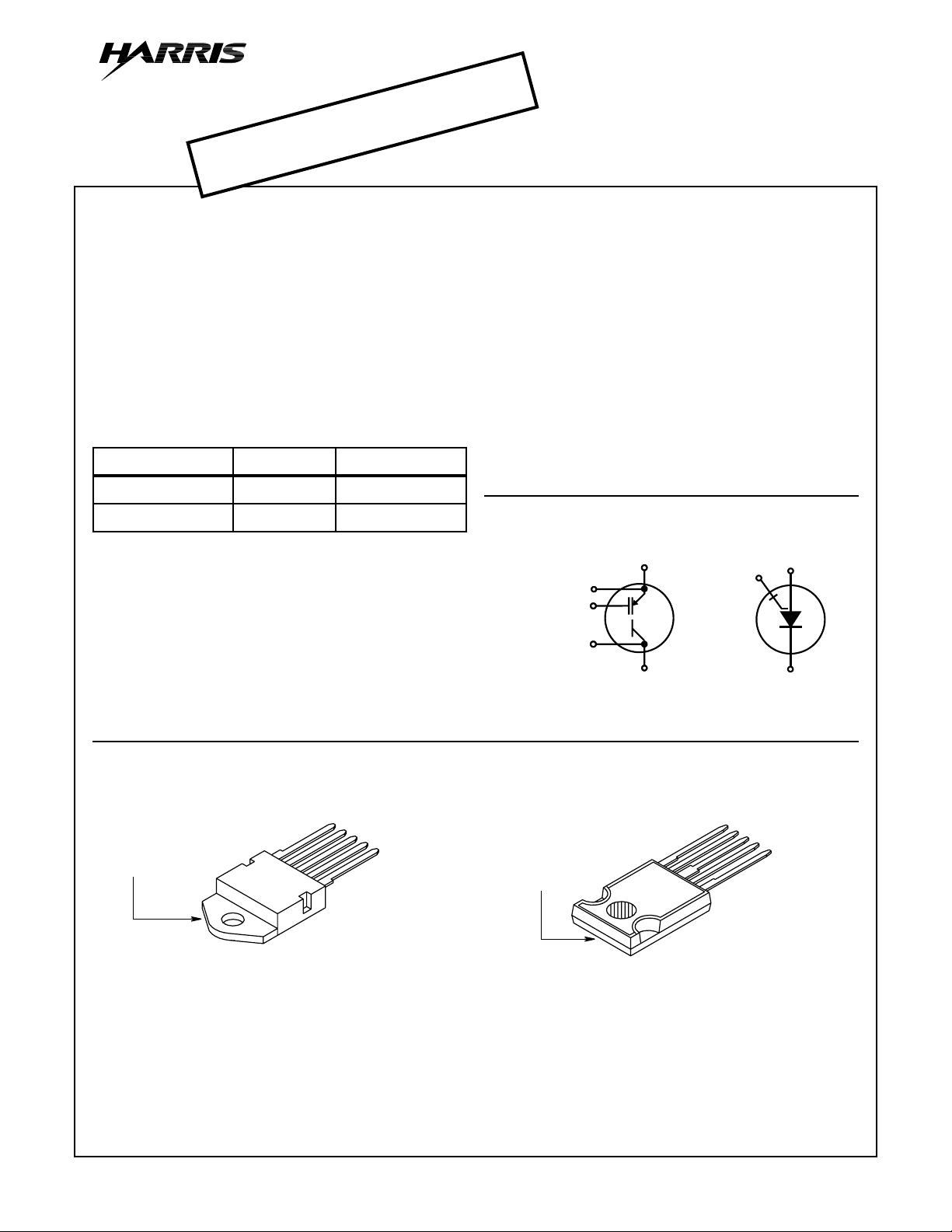
MCT3A65P100F2 TO-247 M65P100F2
MCT3D65P100F2 MO-093AA M65P100F2
NOTE: When ordering, use the entire part number.
Packaging
JEDEC MO-093AA JEDEC STYLE TO-247
ANODE
ANODE
CATHODE
CATHODE
(FLANGE)
GATE RETURN
GATE
Description
The MCT is an MOS Controlled Thyristor designed for switching
currents on and off by negative and positive pulsed control of an
insulated MOS gate. It is designed for use in motor controls,
inverters, line switches, and other po wer s witching applications.
The MCT is especially suited for resonant (zero voltage or zero
current switching) applications. The SCR like forward drop
greatly reduces conduction power loss.
MCTs allow the control of high power circuits with very small
amounts of input energy. They feature the high peak current
capability common to SCR type thyristors, and operate at junction temperatures up to 150
Formerly developmental type TA49226.
o
C with active switching.
Symbols
(ANODE KELVIN)
GATE RETURN
GATE
CATHODE
CATHODE
(BOTTOM SIDE
METAL)
ANODE
CATHODE (TAB)
ANODE
GATE
ANODE
CATHODE
ANODE
CATHODE
GATE RETURN
GATE
[
/PageMode
/UseOutlines
/DOCVIEW
CAUTION: These devices are sensitive to electrostatic discharge. Users should follow proper ESD Handling Procedures.
Copyright
© Harris Corporation 1999
1
File Number 4454.2

MCT3A65P100F2, MCT3D65P100F2
Absolute Maximum Ratings T
= 25oC, Unless Otherwise Specified
C
MCT3A65P100F2
MCT3D65P100F2 UNITS
Peak Off-State Voltage. . . . . . . . . . . . . . . . . . . . . . . . . . . . . . . . . . . . . . . . . . . . . . .V
Peak Reverse Voltage . . . . . . . . . . . . . . . . . . . . . . . . . . . . . . . . . . . . . . . . . . . . . . .V
DRM
RRM
-1000 V
5V
Continuous Cathode Current
At TC = 25oC (Package Limited). . . . . . . . . . . . . . . . . . . . . . . . . . . . . . . . . . . . . . . I
= 110oC . . . . . . . . . . . . . . . . . . . . . . . . . . . . . . . . . . . . . . . . . . . . . . . . . . . I
At T
C
Non-repetitive Peak Cathode Current (Note 1) . . . . . . . . . . . . . . . . . . . . . . . . . . . . .I
Peak Controllable Current . . . . . . . . . . . . . . . . . . . . . . . . . . . . . . . . . . . . . . . . . . . . . . I
Gate to Anode Voltage (Continuous) . . . . . . . . . . . . . . . . . . . . . . . . . . . . . . . . . . . . . V
Gate to Anode Voltage (Peak) . . . . . . . . . . . . . . . . . . . . . . . . . . . . . . . . . . . . . . . . . . V
K25
K110
KSM
KC
GA
GA
85 A
65 A
2000 A
100 A
±15 V
±20 V
Rate of Change of Voltage. . . . . . . . . . . . . . . . . . . . . . . . . . . . . . . . . . . . . . . . . . . . .dv/dt Figure 11
Rate of Change of Current . . . . . . . . . . . . . . . . . . . . . . . . . . . . . . . . . . . . . . . . . . . . . di/dt 2000 A/µs
Maximum Power Dissipation . . . . . . . . . . . . . . . . . . . . . . . . . . . . . . . . . . . . . . . . . . . . P
Power Dissipation Derating T
> 25oC . . . . . . . . . . . . . . . . . . . . . . . . . . . . . . . . . . . . . . . 2.32 W/oC
C
Operating and Storage Junction Temperature Range . . . . . . . . . . . . . . . . . . . . T
T
, T
J
STG
Maximum Temperature for Soldering
Leads at 0.063in (1.6mm) from Case for 10s . . . . . . . . . . . . . . . . . . . . . . . . . . . . . . .T
CAUTION: Stresses above those listed in “Absolute Maxim um Ratings” ma y cause permanent damage to the device . This is a stress only rating and oper ation of
the device at these or any other conditions above those indicated in the operational sections of this specification is not implied.
L
290 W
-55 to 150
300
o
C
o
C
NOTES:
1. Maximum Pulse Width of 200µs (Half Sine). Assume TJ(Initial) = 90oC and TJ(Final) = TJ(Max) = 150oC.
Electrical Specifications T
= 25oC, Unless Otherwise Specified
C
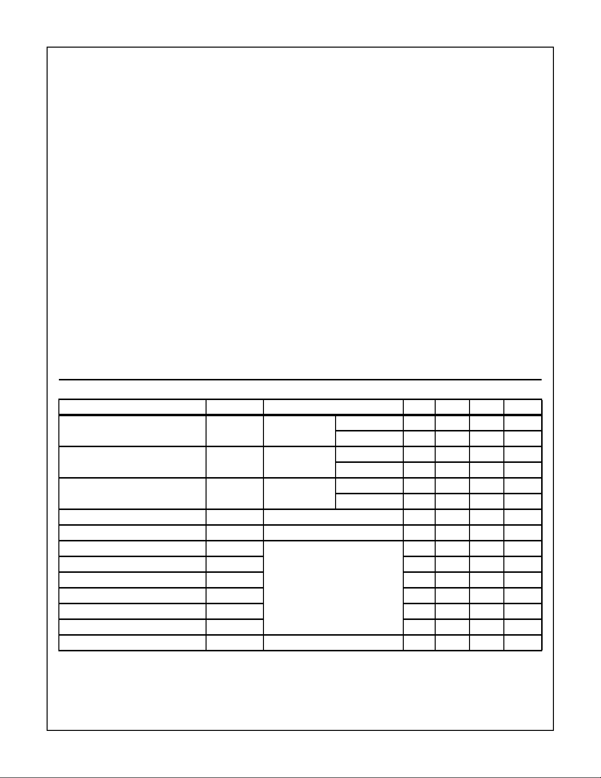
PARAMETER SYMBOL TEST CONDITIONS MIN TYP MAX UNITS
Peak Off-State Blocking Current I
Peak Reverse Blocking Current I
On-State Voltage V
Gate to Anode Leakage Current I
Input Capacitance C
Current Turn-On Delay Time t
d(ON)I
Current Rise Time t
Current Turn-Off Delay Time t
d(OFF)I
Current Fall Time t
Turn-On Energy E
Turn-Off Energy (Note 2) E
Thermal Resistance Junction To Case R
DRM
RRM
TM
GAS
ISS
rI
fI
ON
OFF
θJC
VKA= -1000V
VGA= 15V
VK= 5V
VGA= 15V
IK = I
K110
VGA = -10V
TC = 150oC--3mA
TC = 25oC - - 100 µA
TC = 150oC--4mA
TC = 25oC - - 100 µA
TC = 150oC - 1.25 1.4 V
TC = 25oC - 1.35 1.5 V
VGA = ±20V - - 200 nA
VGA = 15V, VKA = -20V, f = 1MHz - 12 - nF
TC = 150oC
L = 200µH
IK = I
K110
= 65A
VKA = -400V
- 125 - ns
-70- ns
- 770 - ns
VGA = 15V/-10V
RG = 2.2Ω
Test Circuit (Figure 13)
- 1000 1400 ns
- 2.8 - mJ
-15- mJ
- - 0.43
NOTE:
2. Turn-Off Energy Loss (E
) is defined as the integral of the instantaneous power loss starting at the trailing edge of the input pulse and
OFF
ending at the point where the cathode current equals zero (IK = 0A). All devices were tested per JEDEC Standard No. 24-1 Method for
Measurement of Power Device Turn-Off Switching Loss. This test method produces the true total Turn-Off Energy Loss. Turn-On losses
include losses due to diode recovery.
o
C/W
2

MCT3A65P100F2, MCT3D65P100F2
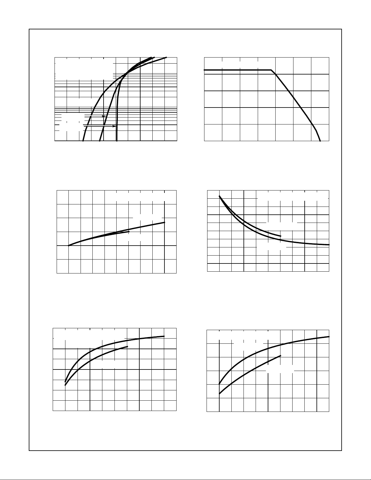
Typical Performance Curves
300
PULSE TEST
PULSE DURATION - 250µs
100
DUTY CYCLE < 2%
10
, CATHODE CURRENT (A)
K
I
1
TJ = 150oC
TJ = 25oC
TJ = -40oC
0 0.2 0.4 0.6 0.8 1.0 1.2 1.4 1.6 1.8 2.0
V
, CATHODE VOLTAGE (V)
TM
(Unless Otherwise Specified)
, DC CATHODE CURRENT (A)
K
I
100
80
60
40
20
0
20 60 80 100 120 140 160
PACKAGE LIMIT
40
T
, CASE TEMPERATURE (oC)
C
FIGURE 1. CATHODE CURRENT vs SATURATION VOLTA GE FIGURE 2. DC CATHODE CURRENT vs CASE TEMPERA TURE
180
160
140
120
100
, TURN-ON DELAY TIME (ns)
80
d(ON)I
t
60
TJ = 150oC, RG = 2.2Ω, L = 200µH
VKA = -400V
VKA = -500V
100 20304050607080 100
I
, CATHODE CURRENT (A)
K
90
2.0
1.8
1.6
1.4
1.2
1.0
0.8
0.6
, TURN-OFF DELAY TIME (µs)
0.4
0.2
d(OFF)i
t
TJ = 150oC, RG = 2.2Ω, L = 200µH
VKA = -500V
VKA = -400V
0
0
10 20 30 40 50 60 70 80 90 100
, CATHODE CURRENT (A)
I
K
FIGURE 3. TURN-ON DELAY TIME vs CATHODE CURRENT FIGURE 4. TURN-OFF DELAY TIME vs CATHODE CURRENT
80
TJ = 150oC, RG = 2.2Ω, L = 200µH
70
60
50
40
30
, RISE TIME (ns)
rI
t
20
10
0
0
VKA = -400V
10 20 30 40 50 60 70 80 90
I
, CATHODE CURRENT (A)
K
VKA = -500V
100
1.2
TJ = 150oC, RG = 2.2Ω, L = 200µH
1.0
0.8
0.6
, FALL TIME (µs)
0.4
fI
t
0.2
0
0
10 20 30 40 50 60 70 80 90 100
VKA = -400V
I
K
VKA = -500V
, CATHODE CURRENT (A)
FIGURE 5. TURN-ON RISE TIME vs CATHODE CURRENT FIGURE 6. TURN-OFF FALL TIME vs CATHODE CURRENT
3
 Loading...